Available online: http://edupediapublications.org/journals/index.php/IJR/ P a g e | 568
Analysis and Design of Current-Fed High Step Up
Quasi-Resonant DC-DC Converter for Fuel Cell Applications
Vasudeva Reddy Yerva
1, V.Sreenivasulu
2,
1P.G. Scholar, 2M.Tech.,
2Assistant Professor, Dept. of EEE.
1,2 SVR ENGINEERING COLLEGE, Kurnool
1Email: - [email protected]
ABSTRACT
In this project a Soft-Switching DC-DC Converter with low voltage and current stresses on switches and high voltage gain is proposed. The voltage and current stresses of switches are considerably reduced. As a result a reduction of switching losses in turn ON and OFF states of switching is obtained. Also, using soft-switching method results lower losses. In the result of ZCS in output diodes, reverse recovery problem of diodes is alleviated. Because of total reduction of losses, efficiency is improved. The proposed converter is a quasi-resonant converter controlled by Pulse Width Modulation (PWM) method.
Keywords:- Pulse Width Modulation, Electromagnetic Interference, Quasi-resonant converters, High Frequency, Zero Current
INTRODUCTION
These days dc-dc converters are more applicable and variety of topologies of them have been proposed. Depend on application of dc-dc converters, different demands are considered like high efficiency [I], [2], high voltage gain [3], low voltage and/or current stress on switches [4] etc. One kind of converter
satisfying these cases is resonant converter [5] [13]. These converters are able to work in high frequencies [14]. Because of this,
these converters have light weight, low ripple and small size. Since in some applications size and weight of converters is highly restricted, resonant converters is more capable. One major disadvantage of resonant converters is their analysis complexity [15], [16].
In high frequencies, Pulse Width Modulation converters have high Electromagnetic Interference (EM!) and switching losses. Resonant converters have low switching losses and EMI in high frequencies [17]. Quasi-resonant converters (QRCs) are a kind of resonant converters employing soft switching at zero voltage (ZVS) and/or zero current (ZCS) to reduce losses and to improve efficiency [4], [18].
Available online: http://edupediapublications.org/journals/index.php/IJR/ P a g e | 569
resonant circuit ZVS happens for switches and ZCS for output diodes. ZCS in voltage doubler circuit alleviates reverse recovery problem of diodes and it's not necessary to fast diode anymore.
Figure 1.1 Proposed Quasi-resonant Converter
2.7 Study of DC-DC Converters
There are a variety of DC-Dc converters are possible. But from the list of the converters only the first four of the converters are to be described which are basically of non-isolated input output terminals.
The buck converter
The buck converter is a commonly used in circuits that steps down the voltage level from the input voltage according to the requirement. It has the advantages of simplicity and low cost. Figure 1 shows a buck converter the operation of the Buck converters start with a switch that is open (so no current flow through any part of circuit) When the switch is closed, the current flows through the inductor, slowly at first, but building up over time. When the switch is closed the inductor pulls current through the diode, and this means the voltage at the inductors "output" is lower than it first was. This is the very basic principle of operation of buck circuit.
Figure 2.1 BUCK Converter
Available online: http://edupediapublications.org/journals/index.php/IJR/ P a g e | 570
1. The circuit is operating in the steady state.
2. The inductor current is continuous (always positive)
3. The capacitor is very large, and the output voltage is held constant at voltage Vo. This restriction will be relaxed later to show the effects of finite capacitance.
4. The switching period is T, the switch is closed for time DT and open for time (1-D)T 5. The components are ideal
The key to the analysis for determining the voltage Vo is to examine the inductor current and inductor voltage first for the switch closed and then for the switch open. The net change in inductor current over one period must be zero for steady state operation. The average inductor voltage is zero. There are two types of operational mode for this circuit a) Continuous Conduction Mode and b) Discontinuous Conduction Mode. They are described below.
Continuous Conduction Mode
A buck converter operates in continuous mode if the current through the inductor (IL) never falls to zero during the commutation cycle. In this mode, the operating principle is described by the chronogram in Figure 1.
Figure. 2.2: The two circuit configurations of a buck converter: (a) On-state, when the switch is closed, and (b) Off-state, when the switch is open
· When the switch pictured above is closed (On-state, top of Figure 2), the voltage across the inductor is VL = Vi − Vo. The current through the inductor rises linearly. As the diode is reverse-biased by the voltage source V, no current flows through it;
· When the switch is opened (off state, bottom of figure 2), the diode is forward biased. The voltage across the inductor is VL = − Vo (neglecting diode drop). Current IL decreases.
The energy stored in inductor L is
Available online: http://edupediapublications.org/journals/index.php/IJR/ P a g e | 571
Therefore, it can be seen that the energy stored in L increases during On-time (as IL increases) and then decreases during the Off-state. L is used to transfer energy from the input to the output of the converter.The rate of change of IL can be calculated from:
……….. (2.2)
With VL equal to Vi − Vo during the On-state and to − Vo during the Off-state. Therefore, the increase in current during the On-state is given by:
t{on}=DT…….. (2.3)
Identically, the decrease in current during the Off-state is given by:
, {off}= T ……(2.4)
If we assume that the converter operates in steady state, the energy stored in each component at the end of a commutation cycle T is equal to that at the beginning of the cycle. That means that the current IL is the same at t=0 and at t=T (see Figure3).So we can write from the above equations:
… (2.5)
It is worth noting that the above integrations can be done graphically: In Figure
3, is proportional to the area of the yellow surface, and to the area of the orange surface, as these surfaces are defined by the inductor voltage (red) curve. As
these surfaces are simple rectangles, their areas can be found easily: for the yellow rectangle and − Votoff for the orange one. For steady state operation, these areas must be equal. As can be seen on figure 4, and . D is a scalar called the duty cycle
with a value between 0 and 1. This yield:
…… (2.6)
Available online: http://edupediapublications.org/journals/index.php/IJR/ P a g e | 572
Figure 2.3 Evolution of the voltages and currents with time in an ideal buck converter operating in continuous mode
In some cases, the amount of energy required by the load is small enough to be transferred in a time lower than the whole commutation period. In this case, the current through the inductor falls to zero during part of the period. The only difference in the principle described above is that the inductor is completely discharged at the end of the commutation cycle (Figure 4). This has, however, some effect on the previous equations.
Fig. 2.4 Evolution of the voltages and currents with time in an ideal buck converter operating in discontinuous mode.
We still consider that the converter operates in steady state. Therefore, the energy in the inductor is the same at the beginning and at the end of the cycle (in the case of discontinuous mode, it is zero). This means that the average value of the inductor voltage (VL) is zero; i.e., that the area of the yellow and orange rectangles in figure 5 are the same. This yields:
….. (2.7) So the value of δ is:
…………..(2.8)
The output current delivered to the load (Io) is constant; as we consider that the output capacitor is large enough to maintain a constant voltage across its terminals during a commutation cycle. This implies that the current flowing through the capacitor has a zero average value. Therefore, we have:
Available online: http://edupediapublications.org/journals/index.php/IJR/ P a g e | 573
Where is the average value of the inductor current. As can be seen in figure 5, the inductor current waveform has a triangular shape. Therefore, the average value of IL can be sorted out geometrically as follow:
…..(2.10)
The inductor current is zero at the beginning and rises during ton up to ILmax. That means that ILmax is equal to:
…………..(2.11)
Substituting the value of ILmax in the previous equation leads to:
…………..(2.12)
And substituting δ by the expression given above yields:
…..(2.13) This expression can be rewritten as:
…………..(2.14)
It can be seen that the output voltage of a buck converter operating in discontinuous mode is much more complicated than its counterpart of the continuous mode. Furthermore, the output voltage is now a function not only of the input voltage (Vi) and the duty cycle D, but also of the inductor value (L), the commutation period (T) and the output current (Io).
Fig. 2.7 Waveforms of current and voltage in a boost converter operating in continuous mode.
Available online: http://edupediapublications.org/journals/index.php/IJR/ P a g e | 574
When a boost converter operates in continuous mode, the current through the inductor (IL) never falls to zero. Figure 3 shows the typical waveforms of currents and voltages in a converter operating in this mode. The output voltage can be calculated as follows, in the case of an ideal converter (i.e. using components with an ideal behaviour) operating in steady conditions:
During the On-state, the switch S is closed, which makes the input voltage (Vi) appear across the inductor, which causes a change in current (IL) flowing through the inductor during a time period (t) by the formula:
…………..(2.15) At the end of the On-state, the increase of IL is therefore:
……..(2.16)
D is the duty cycle. It represents the fraction of the commutation period T during which the switch is On. Therefore D ranges between 0 (S is never on) and 1 (S is always on).
During the Off-state, the switch S is open, so the inductor current flows through the load. If we consider zero voltage drop in the diode, and a capacitor large enough for its voltage to remain constant, the evolution of IL is:
…………..(2.17)
Therefore, the variation of IL during the Off-period is:
..(2.18)
As we consider that the converter operates in steady-state conditions, the amount of energy stored in each of its components has to be the same at the beginning and at the end of a commutation cycle. In particular, the energy stored in the inductor is given by:
…………..(2.19)
So, the inductor current has to be the same at the start and end of the commutation cycle. This means the overall change in the current (the sum of the changes) is zero:
…………..(2.20)
Substituting and by their expressions yields:
Available online: http://edupediapublications.org/journals/index.php/IJR/ P a g e | 575
…………..(2.22)
Which in turns reveals the duty cycle to be:
…………..(2.23)
From the above expression it can be seen that the output voltage is always higher than the input voltage (as the duty cycle goes from 0 to 1), and that it increases with D, theoretically to infinity as D approaches 1. This is why this converter is sometimes referred to as a step-up
converter.
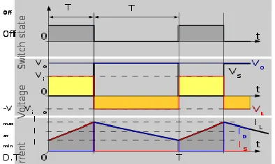
Discontinuous mode
Fig. 2.8. Waveforms of current and voltage in a boost converter operating in discontinuous mode.
In some cases, the amount of energy required by the load is small enough to be transferred in a time smaller than the whole commutation period. In this case, the current through the inductor falls to zero during part of the period. The only difference in the principle described above is that the inductor is completely discharged at the end of the commutation cycle (see waveforms in figure 4). Although slight, the difference has a strong effect on the output voltage equation. It can be calculated as follows:
As the inductor current at the beginning of the cycle is zero, its maximum value (at t =
DT) is
…………..(2.24)
During the off-period, IL falls to zero after δT:
…………..(2.24) Using the two previous equations, δ is:
Available online: http://edupediapublications.org/journals/index.php/IJR/ P a g e | 576
The load current Io is equal to the average diode current (ID). As can be seen on figure 4, the diode current is equal to the inductor current during the off-state. Therefore the output current can be written as:
…………..(2.26)
Replacing ILmax and δ by their respective expressions yields:
…………..(2.27)
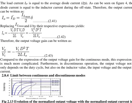
Therefore, the output voltage gain can be written as follows:
…………..(2.28)
Compared to the expression of the output voltage for the continuous mode, this expression is much more complicated. Furthermore, in discontinuous operation, the output voltage gain not only depends on the duty cycle, but also on the inductor value, the input voltage, the switching frequency, and the output current.
2.8 BUCK-BOOST CONVERTER
Another basic switched mode converter is the boost converter. The output of the buck-boost converter can be either higher or lower than the input voltage. Assumption made about the operation of this circuit is same as it was for the previous converter circuits.
2.8.1 Principle of operation
Available online: http://edupediapublications.org/journals/index.php/IJR/ P a g e | 577 Figure 2.10 The two operating states of a buck–boost converter: When the switch is turned-on, the input voltage source supplies current to the inductor, and the capacitor supplies current to the resistor (output load).When the switch is opened, the inductor supplies current to the load via the diode D.
The basic principle of the buck–boost converter is fairly simple (Figure 10):
while in the On-state, the input voltage source is directly connected to the inductor (L). This results in accumulating energy in L. In this stage, the capacitor supplies energy to the output load.
while in the Off-state, the inductor is connected to the output load and capacitor, so energy is transferred from L to C and R. Compared to the buck and boost converters, the characteristics of the buck–boost converter are mainly:
polarity of the output voltage is opposite to that of the input;
The output voltage can vary continuously from 0 to (for an ideal converter). The output voltage ranges for a buck and a boost converter are respectively 0 to and to .The circuit has two
main mode of operations. They are described below.
2.8.2 Continuous mode
Fig 2.11 Waveforms of current and voltage in a buck–boost converter operating in continuous mode.
Available online: http://edupediapublications.org/journals/index.php/IJR/ P a g e | 578
If the current through the inductor L never falls to zero during a commutation cycle, the converter is said to operate in continuous mode. The current and voltage waveforms in an ideal converter can be seen in Figure 3.
From to , the converter is in On-State, so the switch S is closed. The rate of change in the inductor current (IL) is therefore given by
…………..(2.29)
At the end of the On-state, the increase of IL is therefore:
…………..(2.30)
D is the duty cycle. It represents the fraction of the commutation period T during which the switch is On. Therefore D ranges between 0 (S is never on) and 1 (S is always on).
During the Off-state, the switch S is open, so the inductor current flows through the load. If we assume zero voltage drop in the diode, and a capacitor large enough for its voltage to remain constant, the evolution of IL is:
…………..(2.31)
Therefore, the variation of IL during the Off-period is:
…………..(2.32)
As we consider that the converter operates in steady-state conditions, the amount of energy stored in each of its components has to be the same at the beginning and at the end of a commutation cycle. As the energy in an inductor is given by:
…………..(2.33)
it is obvious that the value of IL at the end of the Off state must be the same as the value of IL at the beginning of the On-state, i.e. the sum of the variations of IL during the on and the off states must be zero:
…………..(2.34)
Substituting and by their expressions yields:
Available online: http://edupediapublications.org/journals/index.php/IJR/ P a g e | 579
…………..(2.36) This in return yields that:
…………..(2.37)
From the above expression it can be seen that the polarity of the output voltage is always negative (as the duty cycle goes from 0 to 1), and that its absolute value increases with D, theoretically up to minus infinity as D approaches 1. Apart from the polarity, this converter is either step-up (as a boost converter) or step-down (as a buck converter). This is why it is referred to as a buck–boost converter.
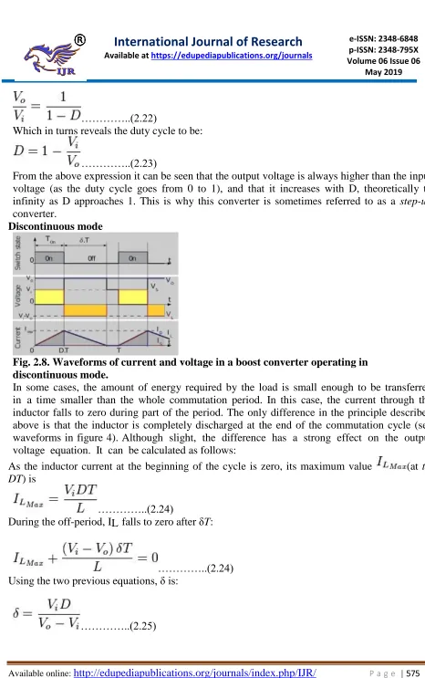
2.8.3 Discontinuous Mode
Fig 2.12 Waveforms of current and voltage in a buck–boost converter operating in discontinuous mode.
In some cases, the amount of energy required by the load is small enough to be transferred in a time smaller than the whole commutation period. In this case, the current through the inductor falls to zero during part of the period. The only difference in the principle described above is that the inductor is completely discharged at the end of the commutation cycle (see waveforms in figure 4). Although slight, the difference has a strong effect on the output voltage equation. It can be calculated as follows:
As the inductor current at the beginning of the cycle is zero, its maximum value (at ) is
…………..(2.38)
During the off-period, IL falls to zero after δ.T:
…………..(2.39) Using the two previous equations, δ is:
Available online: http://edupediapublications.org/journals/index.php/IJR/ P a g e | 580
The load current Io is equal to the average diode current (ID). As can be seen on figure 4, the diode current is equal to the inductor current during the off-state. Therefore, the output current can be written as:
…………..(2.41)
Replacing and δ by their respective expressions yields:
…………..(2.42) Therefore, the output voltage gain can be written as:
…………..(2.43)
Compared to the expression of the output voltage gain for the continuous mode, this expression is much more complicated. Furthermore, in discontinuous operation, the output voltage not only depends on the duty cycle, but also on the inductor value, the input voltage and the output current.
2.8.4 Limit between continuous and discontinuous modes
Fig 2.13 Evolution of the normalized output voltage with the normalized output current in a buck–boost converter.
As told at the beginning of this section, the converter operates in discontinuous mode when low current is drawn by the load, and in continuous mode at higher load current levels. The limit between discontinuous and continuous modes is reached when the inductor current falls to zero exactly at the end of the commutation cycle. with the notations of figure 4, this corresponds to :
…………..(2.44)
…………..(2.45)
In this case, the output current (output current at the limit between continuous and discontinuous modes) is given by:
…………..(2.46)
Replacing by the expression given in the discontinuous mode section yields:
Available online: http://edupediapublications.org/journals/index.php/IJR/ P a g e | 581
As is the current at the limit between continuous and discontinuous modes of operations, it satisfies the expressions of both modes. Therefore, using the expression of the output voltage in continuous mode, the previous expression can be written as:
……..(2.48) Let's now introduce two more notations:
The normalized voltage, defined by . It corresponds to the gain in voltage of the converter;
The normalized current, defined by . The term is equal to the maximum increase of the inductor current during a cycle; i.e., the increase of the inductor current with a duty cycle D=1. So, in steady state operation of the converter, this means that equals 0 for no output current, and 1 for the maximum current the converter can deliver.
Using these notations, we have:
In continuous mode, ;
In discontinuous mode, ;
the current at the limit between continuous and discontinuous mode is
. Therefore the locus of the limit between continuous
and discontinuous modes is given by .
These expressions have been plotted in figure 5. The difference in behaviour between the continuous and discontinuous modes can be seen clearly.
2.9 The CUK Converter:
The Cuk converter is used for getting the output voltage with different polarity. That means output voltage magnitude can be either larger or smaller than the input, and there is a polarity reversal on the output.
The inductor on the input acts as a filter for the dc supply, to prevent large harmonic current. Unlike the previous converter topologies where energy transfer is associated with the inductor. Energy transfer for the cuk converter depends on the capacitor C1. The primary assumptions for this circuit analysis are as before. It also has two modes of operation which are described below.
Available online: http://edupediapublications.org/journals/index.php/IJR/ P a g e | 582
Fig 2.14: Schematic of a non-isolated Ćuk converter.
Figure 2.15: The two operating states of a non-isolated Ćuk converter.
Fig 2.16 : The two operating states of a non-isolated Ćuk converter. In this figure, the diode and the switch
are either replaced by a short circuit when they are on or by an open circuit when they are off. It can be seen that when in the Off state, the capacitor C is being charged by the input source through the inductor L1. When in the On state, the capacitor C transfers the energy to the output capacitor through the inductance L2.
A non-isolated Ćuk converter comprises two inductors, two capacitors, a switch (usually a transistor), and a diode. Its schematic can be seen in figure 1. It is an inverting converter, so the output voltage is negative with respect to the input voltage.
The capacitor C is used to transfer energy and is connected alternately to the input and to the output of the converter via the commutation of the transistor and the diode (see figures 2 and 3).
Available online: http://edupediapublications.org/journals/index.php/IJR/ P a g e | 583
limited only by (parasitic) resistance, resulting in high energy loss. Charging a capacitor with a current source (the inductor) prevents resistive current limiting and its associated energy loss. As with other converters (buck converter, boost converter, buck-boost converter) the Ćuk converter can either operate in continuous or discontinuous current mode. However, unlike these converters, it can also operate in discontinuous voltage mode (i.e., the voltage across the capacitor drops to zero during the commutation cycle).
2.9.2 Continuous mode
In steady state, the energy stored in the inductors has to remain the same at the beginning and at the end of a commutation cycle. The energy in an inductor is given by:
…………..(2.49)
This implies that the current through the inductors has to be the same at the beginning and the end of the commutation cycle. As the evolution of the current through an inductor is related to the voltage across it:
…………..(2.50)
it can be seen that the average value of the inductor voltages over a commutation period have to be zero to satisfy the steady-state requirements.
If we consider that the capacitors C and Co are large enough for the voltage ripple across them to be negligible, the inductor voltages become:
In the off-state, inductor L1 is connected in series with Vi and C (see figure 2). Therefore
VL1 = Vi − VC. As the diode D is forward biased (we consider zero voltage drop), L2 is directly connected to the output capacitor. Therefore VL2 = Vo
In the on-state, inductor L1 is directly connected to the input source. Therefore VL1 = Vi. Inductor L2 is connected in series with C and the output capacitor, so VL2 = Vo + VC
The converter operates in on-state from t=0 to t=D·T (D is the duty cycle), and in off state from D·T to T (that is, during a period equal to (1-D)·T). The average values of VL1 and VL2 are therefore:
….(2.51)
…………..(2.52)
As both average voltage have to be zero to satisfy the steady-state conditions we can write, using the last equation:
…………..(2.53)
So the average voltage across L1 becomes:
Available online: http://edupediapublications.org/journals/index.php/IJR/ P a g e | 584
Which can be written as:
…………..(2.55)
It can be seen that this relation is the same as that obtained for the Buck-boost converter.
2.9.3 Discontinuous mode
Like all DC-DC converters Cuk converters rely on the ability of the inductors in the circuit to provide continuous current, in much the same way a capacitor in a rectifier filter provides continuous voltage. If this inductor is too small or below the "critical inductance", then the current will be discontinuous. This state of operation is usually not studied too much depth, as it is not used beyond a demonstrating of why the minimum inductance is crucial.
The minimum inductance is given by:
………..(2.56)
Where fs is the switching frequency.
OPERATION PRINCIPLE AND CONVERTER ANALYSIS
Proposed converter circuit is shown in Fig. 1. Input boost circuit consists of inductance LB and switch S1. Leakage inductance of transformer in primary side modelled as Lk. Capacitor C1 and leakage inductance Lk provide resonant circuit. Active clamp circuit is made by C2 and switch S2. In secondary side of the transformer, diodes Dl and D2 work as a half bridge rectifier, providing voltage doubler circuit with capacitors C0l and CO2 in output.
In this converter, parasitic capacitances and Ron resistance of switches are neglected. Because of ZCS on the output diodes, fast diodes are not necessary. Moreover RL is candidate as load resistance, N1 and N2 are primary and secondary of transformer's turn ratio respectively and n is defined as n = N2/N1. fs and fr are switching and resonant frequency respectively.
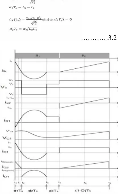
The operation of proposed converter is described by the following six intervals. Important currents and voltage curves in Fig. 2 and circuit diagrams are shown in Fig. 3. At the time before to , switch S2 is turned ON. Inductance LB is large enough to alleviate input current ripple so assume that input current has constant value lin. Further assume that voltage of C2 has constant value VC2.
3.1.1 Interval 1[to, t1]
At to , S2 turns OFF and difference of input and the transformer current flow through anti-parallel diode of switch S1. As long as this current flows, voltage across S1 is zero and gate pulse can be applied to achieve ZVS. This interval will finish when reverse current of S1 decreases to zero.
3.1.2Interval 2[t1, t2]
Available online: http://edupediapublications.org/journals/index.php/IJR/ P a g e | 585
…………3.1 Where V’cl is voltage of capacitor C1 at the time to.
3.1.3 Interval 3 [t2 t3]
At t2 , the transformer current ilk changes its direction and voltage of output capacitor Col is reflected via transformer to the primary side and C1 and Lk make resonance. This interval will fmish when ilk reaches to zero. During this interval, as a result of Vin across the LB, current of input inductance is rising. Because of changing the current of transformer direction in this interval, direction of secondary current is also changed, so in output doubler circuit, D1 is conducting and supplies output capacitor C0l. For this interval:
…………3.2
Figure 3.1 Operating Waveforms Of Quasi Resonant Converter
Where Vo1/n is voltage of capacitor C0l. reflected to the primary side of the transformer.
3.1.4 Interval 4 [t3 t4]
Available online: http://edupediapublications.org/journals/index.php/IJR/ P a g e | 586
and capacitor C1 reach zero too, but the current of S1 remains lin in the entire interval and the power supply charges the inductor LB. Based on the diagrams shown in Fig. 2 :
…………3.3 And, by applying volt-second law to the transformer winding:
…………3.4
Figure 3.2 Operating Intervals of Quasi Resonant Converter
In the output, diodes are turned OFF because secondary current is zero. So in this interval output capacitors (COl and CO2) supply the load.
Interval 5 [t4 t5]
Available online: http://edupediapublications.org/journals/index.php/IJR/ P a g e | 587
across S2 is zero and gate pulse can be applied to achieve ZVS. In output, D2 is conducting and supplies output capacitor CO2. This interval will finish when reverse current of S2 reaches zero.
Interval 6 [t5 t6]
When current of anti-parallel diode of S2 reaches to zero, its direction changes, and it flows through switch S2 which has been turned ON in previous interval. The current of transformer is rising just like previous interval. In these two later intervals, input constant current flows through the transformer and charges Cl. Current of capacitor C2 circulates through the transformer.
This Interval finishes by removing pulse gate of S2. The current of transformer rises linearly from 0 until at the time t6 reaches to the il . So:…………3.5
VC2 is voltage of clamp capacitor and V02/n is voltage of CO2 on the output which was reflected to the primary side of the transformer, and DTs is duty cycle of switch S1· To achieve minimum current stress in Turn-OFF switching state, this proposed converter works in discontinues conduction mode. Further controllability of converter becomes easier. In contrast with conventional resonant converters this proposed converter can be controlled with PWM method. Consequently, converter works in constant frequency reducing EMI effect [19]. Since this converter is controlled by PWM method the control complexity is eliminated.
This proposed converter has a boost circuit on the input with large inductance causing low input ripple. The leakage inductance of transformer is used for resonant inductance of resonant circuit. An active clamp circuit is implemented parallel with primary side of the transformer to clamp primary side voltage. In secondary side of transformer, voltage doubler circuit is used to achieve high voltage gain.
THEORETICAL ANALYSIS Voltage Gain
Here it is assumed that voltage of capacitors C1 , C2 and C0l, and input current lin are constant.
According to proposed converter in Fig. 1, by applying KCL to node "a", average current of C1, C2 and Lk is zero.
…………4.1
Where "(.)" means, average value of "." here. In steady state, average current of capacitors is zero, So:
…………4.2 But during the time (1 - D)Ts = t6 - t4, by applying KCL in node “b”.
Available online: http://edupediapublications.org/journals/index.php/IJR/ P a g e | 588
Here lin is average input current. Switch S2 is in series with capacitor C2 (iC2 = iS2) so from (12) it's average current is zero. Form Fig. 2 during the time(l - D)Ts, average current of iLk is equal to lin, then:
…………4.4
By applying KVL:
…………4.5
In steady state average voltage of inductors and the windings of transformer are zero, so:
…………4.6
As shown in Fig. 3 at the time t4 to t6 the current lin flows through C1 and then current of C1 jumps to i1 after that decreases almost linearly to zero, simultaneously voltage of C1 during the time t4 to t6 increases linearly and after that it resonance and reaches its peak at t2, its minimum happened at t3 and it would be constant to the end of time period.
Voltage of C1 increases linearly during t4 to t6. The time interval between to to t2 is too short, consequently It can be assumed that in this interval voltage of C1 is constant. So from (IS) it can be said:
…………4.7
Figure 4.1 Output Diode Current
From FigA and by applying volt-second product equations on output capacitors, relations between V0l, V02 and VO can be easily obtained as following [20]:
…………4.8
Available online: http://edupediapublications.org/journals/index.php/IJR/ P a g e | 589
…………4.9
From(1),(9),(20),(21) and (23), T1 can be obtained as follow:
…………4.10
Average current of each output diodes is equal to output current, because average current capacitors are zero. So:
…………4.11
By using (9),(25) and (27) output current can be obtained as follow:
………4.12 Form (28) voltage gain can be expressed as:
Available online: http://edupediapublications.org/journals/index.php/IJR/ P a g e | 590 Figure 4.2 simulated waveforms of proposed converter (a) VT and Vgs1 ,10V/div.(b) ILK,
5V/div. (c) is1 and is2, 10V/div. (d) iD1 and iD2, 1A/div. (e) Iin, 10A/div
4.1.2 Input current ripple
Available online: http://edupediapublications.org/journals/index.php/IJR/ P a g e | 591
…………4.13
Maximum switches voltage
As we assumed before, voltage of C1 between to to t2 is constant. Voltage of S1 rises linearly to its peak, and turn OFF and S2 turn ON. After that, voltage of S2 decreases sinusoidal until t3. So it can be assumed that both switches maximum voltage is equal. By applying KVL on S1,S2, C1 and C2 at to:
…………4.13
SIMULATION RESULTS
This proposed converter is simulated and simulation waveforms results are shown in Fig. 5. In this simulation example input voltage is Vin = 24v and average input current is Iin = 9A, so output power is Pin = 220w. Here output voltage is Vo = 360v. Switch S1 has duty cycle about D = 0.7. Other converter elements parameter are as follow: LB = 200uH, Lk = 2UH , C2 = 47uF, C1 = luF , COl = CO2 = 10uF , fs = 100KHz and n = 5. In this condition, efficiency of proposed converter is about n = 96%.
In Fig. 6 voltage gain against duty cycle for RL = 800D. and some Lk values is plotted. It's clear that output voltage changes by duty cycle so by controlling duty cycle, output voltage can be regulated.
Efficiency of converter has been shown in Fig. 7 at various output power. It can be seen that in output power about 30w to 330w converter efficiency varies in region between 95% and 98%.
Figure 5.1 Measured Output Voltage at different duty cycle
Available online: http://edupediapublications.org/journals/index.php/IJR/ P a g e | 593 CONCLUSION
In this paper, the steady state analysis of a new quasi- resonant converter for fuel cell application has been presented. Since this converter works in discontinuous conduction mode, switches stress have been minimized. These switches are working under ZVS condition which cause low switching losses. The leakage of transformer Lk inductance has been employed to made the resonant circuit with C1. Therefore, an active clamp circuit across the primary side of the transformer clamps its primary voltage. Using a boost circuit with a large inductor in the input of converter cause low input current ripple which is appropriate for fuel cell applications. In output, a voltage doubler circuit has been used to obtain high voltage gain. The output diodes working under ZCS, alleviate their reverse recovery problem and reduce losses. By these reduction of losses, converter has a high efficiency.
Available online: http://edupediapublications.org/journals/index.php/IJR/ P a g e | 594
[1] 1. M. Kwon�E. H. Kim. B. H. Kwon and K. H. Nam, "High-Efliciency Fuel Cell Power Conditioning System With Input Current Ripple Reduction," IEEE Trans. Ind. Electron. Vol. 56 , no. 3, pp. 826 - 834, October 2008.
[2] S. H. Cho, C. S. Kim, and S. K. Han, "High-Efficiency and Low-Cost Tightly Regulated Dual-Output LLC Resonant Converter," IEEE Trans. Ind. Electrons. , Vol. 59, no. 7, pp.2982-2991, July 2012.
[3] A. Shahin, M. Hinaje, J. P. Martin, S. Pierfederici, S. Rae!, and Bernard Davat, "High Voltage Ratio DC-DC Converter for Fuel-Cell Applications," Power Electronics Specialists Conference, pp.1277-1283, June 2008. [4] R.1. Wai, C.Y. Lin, L.W. Liu and R.Y. Duan "Voltage-clamped forward quasi-resonant converter with soft
switching and reduced switch stress," IEE Proc. Electric Power Applications. , Vol. 152, no. 3, pp.558-564, May 2005.
[5] Y. K. Lo, C. Y. Lin, M. T. Hsieh and C. Y. Lin, "Phase-Shifted Full- Bridge Series-Resonant DC-DC Converters for Wide Load Variations," IEEE Trans. Ind. Electron. Vol. 58 , no. 6, pp. 2572 - 2575, June 2011. [6] S.S. Tanavade, H.M. Suryawanshi, K.L. Thakre and M.A. Chaudhari, "Application of three-phase
resonant converter in high power DC supplies," lEE Proc., Electric Power Applications, Vol. 152, no.6, pp.1401-1409, Nov. 2005.
[7] B. C. Hyeon, and B. H. Cho, "Analysis and Design of the Lm C Resonant Converter for Low Output Current Ripple," IEEE Trans. Ind. Electron. Vol. 59, no.7, pp-2771-2780, July 2012.
[8] RJ. Wai, c.Y. Lin, L.W. Liu and R.Y. Duan "Voltage-clamped forward quasi-resonant converter with soft switching and reduced switch stress," IEE Proc. Electric Power Applications, Vol. 152, no.3, pp.558-564, May 2005.
[9] K. 1. Lee, B. G. Park, R. Y. Kim and D. S. Hyun, "Nonisolated ZVT Two-Inductor Boost Converter With a Single Resonant Inductor for High Step-Up Applications" Power Electronics and ECCE Asia (ICPE & ECCE), 2011 IEEE 8th International Conference, pp.1785-1792, May & June 2013.
[10] X. Li, and A. K. S. Bhat, "Analysis and Design of High-Frequency Isolated Dual-Bridge Series Resonant DC/DC Converter," IEEE Trans. on Power Electron. , Vol 25, no A, pp.850-862, April 201 [11] W. Chen, P. Rong and Z. Lu, "Snubberless Bidirectional DC-DC Converter With New CLLC
Resonant Tank Featuring Minimized Switching Loss," IEEE Trans. On Ind. Electron. , Vol. 57, no. 9, pp.3075-3085, Sept. 2010.
[12] W. Chen, P. Rong and Z. Lu, "Investigation on Topology for Type-4 LLC Resonant Dc-Dc Converter," IEEE Trans. On Ind. Electron. , Vol. 57, no. 9, Sept. 2010.
[13] F. C. Lee, S. Wang, P. Kong, C. Wang and D. Fu, "Power Architecture Design with Improved System Efficiency, EMI and Power Density," Power Electronics Specialists Conference, ppA13 1-4137, June 2008. [14] J. Hu, A. D. Sagneri, J. M. Rivas, Y. Han, S. M. Davis, and D. J. Perreault, "High-Frequency
Resonant SEPIC Converter With Wide Input and Output Voltage Ranges," IEEE Trans. on Power Electron. , Vol 27, no.l, pp.189-200, Jan. 2012.
[15] W. J. GU AND K. HARADA, "A New Method to Regulate Resonant Converters," IEEE Trans. on Power Electron. , Vol 3, noA, ppA30-439, Oct. 1988.
[16] N. Shafiei, M. Pahlevaninezhad, H. Farzanehfard, A. Bakhshai and P. Jain, "Analysis of a Fifth-Order Resonant Converter for High-Voltage DC Power Supplies," IEEE Trans. on Power Electron. , Vol 28, no.I, pp.85-100, Jan. 2013.
[17] B. R. Lin, and 1. Y. Dong "ZVS Resonant Converter With Parallel- Series Transformer Connection," IEEE Trans. on Ind. Electron. , Vol. 58, no. 7, pp.2971-2979, July 2011.
[18] Y. S. Lee and Y. Y. Chiu "Zero-current-switching switched-capacitor bidirectional DC-DC converter," lEE Proc. Electric Power Applications. , Vol. 152, no. 6, pp.1525-l530, Nov. 2005.
[19] W. 1. Lee, S. W. Choi,C. E. Kim and G. W. Moon, "A New PWM- Controlled Quasi-Resonant Converter for a High Efficiency PDP Sustaining Power Module," IEEE Trans. on Power Electron. , Vol 23, noA, pp.1782-1790, July 2008.