© 2015, IRJET.NET- All Rights Reserved
Page 782
Closed Loop Control of Single-Input Multiple-Output DC–DC Converter
B.Uma MaheswaraRao
1,K.Nagalingachari
2,L.Sri ram
3M.Tech scholar, Department of EEE LakkiReddyBaliReddy College of engineering,Vijayawada, India.
Assistant professor, Department of EEE, LakkiReddyBaliReddy College of engineering, Vijayawada, India.
M. Tech scholar, Department of EEE LakkiReddyBaliReddy College of engineering, Vijayawada, India.
Abstract:- The aim of this study is to develop a closed
loop single-input multiple-output (SIMO) dc–dc converter. The proposed converter can increase the voltage of a low level voltage input power source to a controllable high level voltage dc bus and mid-level voltage output terminals. The high level voltage dc bus can take as the main power for a high level voltage dc load or for a dc–ac inverter. Moreover, mid-level voltage output terminals can supply powers for individual mid-level voltage dc loads or for charging auxiliary power sources (e.g., battery modules). In this study, a coupled-inductor based dc–dc converter utilizes only one power switch with the corresponding device specifications are adequately designed. As a result, the objectives of high-efficiency power conversion, high step up ratio, and various output voltages with different levels can be achieved.Index Terms
:-
Coupled inductor, power conversion,single-input multiple-output (SIMO) converter voltage clamping.
I.INTRODUCTION
In order to protect the natural environment on the earth, the development of clean energy without pollution has themajor representative role in the last decade [1]–[3]. By dealing with the issue of global warming, clean energies, such as fuel cell (FC), photovoltaic, and wind energy, etc., have been rapidly promoted. Due to the electric characteristics of clean energy, the generated power is critically affected by the climate or has slow transient responses, and the output voltage is easily influenced by load variations [4]–[6]. Besides, other auxiliary components, e.g., storage elements, control boards, etc., are usually required to ensure the proper operation of clean energy. For example, an FC-generation system is one of the most efficient and effective solutions to the environmental pollution problem [7]. In addition to the FC stack itself, some
© 2015, IRJET.NET- All Rights Reserved
Page 783
power switch with a small RD S(on) . Because the slew rate of
the current change in the coupled inductor can be restricted by the leakage inductor, the current transition time enables the power switch to turn ON with the ZCS property easily, and the effect of the leakage inductor can alleviate the losses caused by the reverse-recovery current. Additionally, the problems of the stray inductance energy and reverse-recovery currents within diodes in the conventional boost converter also can be solved, so that the high-efficiency power conversion can be achieved. The voltages of middle-voltage output terminals can be appropriately adjusted by the design of auxiliary inductors; the output voltage of the high-voltage dc bus can be stably controlled by a simple proportional-integral (PI) control. This study is mainly organized into five sections. Following the introduction, the converter design and analyses are given in Section II. In Section III, the design considerations of the proposed SIMO converter are discussed in detail. Section IV provides simulation results of proposed converter.
II. CONVERTER DESIGN AND ANALYSES
The system configuration of the proposed high-efficiency SIMO converter topology to generate two different voltage levels from a single-input power source is depicted in Fig. 1. This SIMO converter contains five parts including a low-voltage-side circuit (LVSC), a clamped circuit, a middle-voltage circuit, an auxiliary circuit, and a high-middle-voltage-side circuit (HVSC). The major symbol representations are summarized as follows. VFC (iFC ) and VO1 (iO1) denote the
voltages (currents) of the input power source and the output load at the LVSC and the auxiliary circuit, respectively; VO2
and iO2 are the output voltage and cur-rent in the HVSC. CFC ,
CO1 , and CO2 are the filter capacitors at the LVSC, the auxiliary
circuit, and the HVSC, respectively; C1and C2are the clamped
and voltage capacitors inthe clamped and middle-voltage circuits, respectively. LP and LSrepresent individual
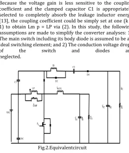
in the HVSC.The corresponding equivalent circuit given in Fig. 2 is used to define the voltage polarities and current directions. The coupled inductor in Fig. 1 can be modelled as an ideal transformer including the magnetizing inductor Lm p and the leakage inductor Lk p in Fig. 2. The turn’s ratio N and coupling coefficient k of this ideal transformer are defined as
N = N2/N1 (1)
k = Lmp/(Lkp + Lmp) = Lmp/LP (2)
Where N1 and N2 are the winding turns in the primary and secondary sides of the coupled inductor Tr .
Fig. 1.System configuration of input multiple-output (SIMO) converter.
Because the voltage gain is less sensitive to the coupling coefficient and the clamped capacitor C1 is appropriately selected to completely absorb the leakage inductor energy [13], the coupling coefficient could be simply set at one (k = 1) to obtain Lm p = LP via (2). In this study, the following assumptions are made to simplify the converter analyses: 1) The main switch including its body diode is assumed to be an ideal switching element; and 2) The conduction voltage drops
© 2015, IRJET.NET- All Rights Reserved
Page 784
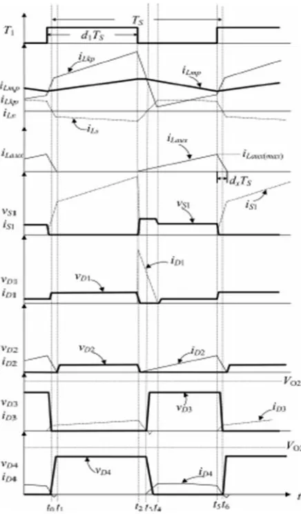
The characteristic waveforms are depicted in Fig. 3, and the topological modes in one switching cycle are illustrated in Fig. 4.
Mode 1 (t0 –t1 ) [Fig. 4(a)]: In this mode, the main switch S1 was turned ON for a span, and the diode D4 turned OFF. Because the polarity of the windings of the coupled inductor Tr is positive, the diode D3 turns ON. The secondary current iL s reverses and charges to the middle-voltage capacitor C2 . When the auxiliary inductor Laux releases its stored energy completely, and the diode D2 turns OFF, this mode ends.
Mode 2 (t1 –t2 ) [Fig. 4(b)]: At time t = t1 , the main switch S1 is persistently turned ON. Because the primary inductor LP is charged by the input power source, the magnetizing current iLmp increases gradually in an approximately linear way. At the same time, the secondary voltage vL s charges the middle-voltage capacitor C2 through the diode D3 . Although the voltage vL m p is equal to the input volt-age VFC both at modes 1 and 2, the ascendant slope of the leakage current of the coupled inductor (diL k p /dt) at modes 1 and 2 is different due to the path of the auxiliary circuit. Because the auxiliary inductor Laux releases its stored energy completely, and the diode D2 turns OFF at the end of mode 1, it results in the reduction ofdiL k p /dt at mode 2.
Mode 3 (t2 –t3 ) [Fig. 4(c)]: At time t = t2 , the main switch S1 is turned OFF. When the leakage energy still released from the secondary side of the coupled inductor, the diode D3 persistently conducts and releases the leakage energy to the middle-voltage capacitor C2 . When the voltage across the main switch vS 1 is higher than the voltage across the clamped capacitor VC 1 , the diode D1 conducts to transmit the energy of the primary-side leakage inductor Lk p into the clamped capacitor C1 . At the same time, partial energy of the primary-side leakage inductor Lk p is transmitted to the auxiliary inductor Laux , and the diode D2 conducts. Thus, the current iL aux passes through the diode D2 to supply the power for the output load in the auxiliary circuit. When the secondary side of the coupled inductor releases its leakage energy completely, and the diode D3 turns OFF, this mode ends.
Mode 4 (t3 –t4 ) [Fig. 4(d)]: At time t = t3 , the main switch S1 is persistently turned OFF. When the leakage energy has released from the primary side of the coupled inductor, the secondary current iL S is induced in reverse from the energy of the magnetizing inductor Lm p through the ideal transformer, and flows through the diode D4 to the HVSC. At the same time, partial energy of the primary-side leakage inductor Lk p is still persistently transmitted to the auxiliary
inductor Laux , and the diode D2 keeps to conduct. Moreover, the current iL aux passes through the diode D2 to supply the power for the output load in the auxiliary circuit.
Fig.3. Characteristic waveforms of high-efficiency SIMO converter.
© 2015, IRJET.NET- All Rights Reserved
Page 785
the HVSC through the diode D4 .
Mode 6 (t5 –t6 ) [Fig. 4(f)]: At time t = t5 , this mode begins when the main switch S1 is triggered. The auxiliary inductor current iL aux needs time to decay to zero, the diode D2 persistently conducts. In this mode, the input power source, the clamped capacitor C1, the secondary winding of the coupledinductor Tr , and the middle-voltage capacitor C2 still connect in series to release the energy into the HVSC through the diode D4 . Since the clamped diode D1 can be selected as a low-voltage Schottky diode, it will be cut off promptly without a reverse-recovery current. Moreover, the rising rate of the primary current iLkp is limited by the primary-side leakage inductor Lkp . Thus, one cannot derive any currents from the paths of the HVSC, the middle-voltage circuit, the auxiliary circuit, and the clamped circuit. As a result, the main switch S1 is turned ON under the condition of ZCS and this soft-switching property is helpful for alleviating the switching loss. When the secondary current iL S decays to zero, this mode ends.
After that, it begins the next switching cycle and repeats the operation in mode 1.
© 2015, IRJET.NET- All Rights Reserved
Page 786
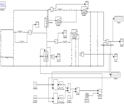
Fig 5 shows the closed loop control of SIMO DC-DC Converter in which both the output voltages are compared with reference values. After comparing, produced error is processed through two PI controllers then two processed signals are averaged and fed to PWM generator. By connecting PWM pulses to the switch of the converter we can get controllable output voltages at output stages. This technique can be used for multiple outputs DC-DC Converter.
SIMO DC-DC Converter
Fig 5 closed loop control
III. SIMULATION RESULTS
In this section the simulation results are presented.
Fig 6 Simulink Model of Proposed SIMO DC-DC Converter
© 2015, IRJET.NET- All Rights Reserved
Page 787
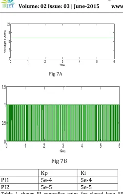
Fig 7A
Fig 7B
Kp
Ki
PI1
5e-4
5e-4
PI2
5e-5
5e-5
Table 1 shows PI controller gains for closed loop SIMO Converter
Fig 8 (a)&(b) shows controlled output voltages at auxiliary circuit and high voltage circuit respectively.
Fig 8A
12 V I/P
Reference
Achieved
V01
21
21.02
V02
205
205.2
Table 2 presents the accuracy of closed loop control of Proposed converter.
IV. CONCLUSION
Proposed converter configuration provides controllable voltage levels at different output terminals.This converter can be used in renewable energy sources like Fuel Cell,Solar,wind etc,.This converter can be connected to any kind of loads and/or inverters are an added advantage.
REFERENCES
[1] A. Kirubakaran, S. Jain, and R. K. Nema, “DSP-controlled power electronic interface for fuel-cell-based distributed generation,” IEEE Trans.Power Electron., vol. 26, no. 12, pp. 3853–3864, Dec. 2011.
[2] B. Liu, S. Duan, and T. Cai, “Photovoltaic
dc-building-module-based BIPV system-concept and design
considerations,” IEEE Trans. Power Electron., vol. 26, no. 5, pp. 1418–1429, May 2011.
© 2015, IRJET.NET- All Rights Reserved
Page 788
[4] C. T. Pan,M. C. Cheng, and C.M. Lai, “A novel integrated dc/ac converter with high voltage gain capability for distributed energy resource systems,” IEEE Trans. Power Electron., vol. 27, no. 5, pp. 2385–2395, May 2012.
[5] S. D. GaminiJayasinghe, D. MahindaVilathgamuwa, and U. K. Madawala, “Diode-clamped three-level inverter-based battery/ supercapacitor direct integration scheme for renewable energy systems,” IEEE Trans. Power Electron., vol. 26, no. 6, pp. 3720–3729, Dec. 2011.
[6] H.Wu, R. Chen, J. Zhang, Y. Xing, H. Hu, and H. Ge, “A family of three port half-bridge converters for a stand-alone renewable power system,” IEEE Trans. Power Electron., vol. 26, no. 9, pp. 2697–2706, Sep. 2012.
[7] M. W. Ellis, M. R. Von Spakovsky, and D. J. Nelson, “Fuel cell systems: Efficient, flexible energy conversion for the 21 st century,” Proc. IEEE, vol. 89, no. 12, pp. 1808–1818, Dec. 2001.
[8] T. Kim, O. Vodyakho, and J. Yang, “Fuel cell hybrid electronic scooter,” IEEE Ind. Appl. Mag., vol. 17, no. 2, pp. 25–31, Mar./Apr. 2011.
[9] F. Gao, B. Blunier, M. G. Sim˜oes, and A. Miraoui, “PEM fuel cell stack modeling for real-time emulation in hardware-in-the-loop application,” IEEE Trans. Energy Convers., vol. 26, no. 1, pp. 184–194, Mar. 2011.
[10] P. Patra, A. Patra, and N. Misra, “A single-inductor multiple-output switcher with simultaneous buck, boost and inverted outputs,” IEEE Trans. Power Electron., vol. 27, no. 4, pp. 1936–1951, Apr. 2012.
[11] A. Nami, F. Zare, A. Ghosh, and F. Blaabjerg, “Multiple-output DC–DC converters based on diode-clamped converters configuration: Topology and control strategy,” IET Power Electron., vol. 3, no. 2, pp. 197–208,2010.
[12] Y. Chen, Y. Kang, S. Nie, and X. Pei, “The multiple-output DC–DC converter with shared ZCS lagging leg,” IEEE Trans. Power Electron., vol. 26, no. 8, pp. 2278–2294, Aug. 2011.
[13] R. J.Wai and R. Y. Duan, “High step-up converter with coupled inductor,” IEEE Trans. Power Electron., vol. 20, no. 5, pp. 1025–1035, Sep. 2005.
[14] N. Mohan, T. M. Undeland, and W. P. Robbins, Power Electronics: Converters, Applications, and Design. New York: Wiley, 1995.
[15] L. Schuch, C. Rech, H. L. Hey, H. A. Gr¨undling, H. Pinheiro, and J. R. Pinheiro, “Analysis and design of a new high-efficiency bidirectional integrated ZVT PWM converter for DC-bus and battery-bank interface,” IEEE Trans. Ind. Appl., vol. 42, no. 5, pp. 1321–1332, Sep./Oct. 2006.
[16] Y. Chen and Y. Kang, “A full regulated dual-output dc-dc converter with special-connected two transformers (SCTTs) cell and complementary pulsewidth modulation-PFM(CPWM-PFM),” IEEE Trans. Power Electron., vol. 25, no. 5, pp. 1296– 1309, May 2010.
[17] J. K. Kim, S.W. Choi, and G.W. Moon, “Zero-voltage switching postregulation scheme for multioutput forward converter with synchronous switches,” IEEE Trans. Ind. Electron., vol. 58, no. 6, pp. 2378–2386, Jun. 2011.
[18] L. Hang, S. Wang, Y. Gu, W. Yao, and Z. Lu, “High cross-regulation multi output LLC series resonant converter with Magamppostregulator,” IEEE Trans. Ind. Electron., vol. 58, no. 9, pp. 3905–3913, Sep. 2011.