Abstract
HUA, HAO. Design and Verification Methodology for Complex Three-Dimensional Digital Integrated Circuit. (Under the guidance of Professor W. Rhett Davis).
Three-Dimensional Integrated Circuits (3DICs) have recently attracted great interest from researchers and IC designers as a possible solution to fill the gap between device and interconnect scaling. Various studies have demonstrated the potential performance improvement of 3DICs by eliminating long interconnects, repeaters, and clock buffers.
Though 3DICs are attractive, there are significant challenges associated with this topic. The most fundamental issue in 3DIC is heat dissipation. The thermal effect has impacted the conventional high-performance 2DICs in deep sub-micron technology nodes. Its effect will aggravate 3DICs due to two major reasons: higher power density, and lower thermal conductivity caused by more insulating dielectric layers. Furthermore, while 3D integration provides more design flexibility, this technology also introduces much higher design complexity. The existing 2D physical design methodology cannot be simply extended to a 3D case because of the huge obstacles in the z-direction and thermal constraints. Efficient design flows and algorithms must be developed to facilitate 3DIC design.
(or databases) of the commercial tools and add 3D features to them. The entire flow achieves RTL-to-GDSII physical design automation for 3DICs.
Design and Verification Methodology for
Complex Three-Dimensional Digital Integrated
Circuit
By
Hao Hua
A dissertation submitted to the Graduate Faculty of North Carolina State University
in partial fulfillment of the requirements for the Degree of
Doctor of Philosophy
E
LECTRIAL
E
NGINEERING
Raleigh, 2006
APPROVED BY:
_____________________ _____________________
W. RHETT DAVIS PAUL D. FRANZON
Chair of Advisor Committee
_____________________ _____________________
Biography
Acknowledgements
I would like to summarize my acknowledgements to the people who have been supporting and collaborating me on the work. Without them, this dissertation would never have been accomplished. I am grateful to be a part of an innovative project, a friendly group, and an enjoyable working environment. I would like to thank the people who gave me this opportunity.
First and foremost, I would like to thank my family: my parents Quanrong and Jingyu, my grandma Rong, my wife Yue, and my coming baby. Their love and support have been my source of inspiration, power, and ambition. Even the physical distance between my (grand)parents and I is great, I can feel a strong tie linking us together. My wife has been encouraging me when I felt depressed, and she has become the sunshine of my life. Without them, I could not imagine how I could ever be able to manage all the difficulties and challenges.
I would like to thank my advisor, Dr. W. Rhett Davis, who brought me into the design automation world and has guided me through my study. I would probably never realize the beauty of VLSI if I had not talked with him. He has also supported me in various aspects. Without him, my dream of being a Ph.D. would never come true.
continuously giving me advice on how to improve my work. Dr. Franzon’s sharp vision on the big picture impressed me every time I had a chance to talk with him.
Next, I would like to take this chance to thank my colleagues and friends. I would like to thank Ravi Jenkal, Samson Melamed, Chris Mineo, Kory Schoenfliess, and Ambarish Sule for their generous support. They have provided all the complementary materials to facilitate my research during my stay. It is always a great pleasure to work with smart people. I also would like to thank Jian Xu and Leon Zhang from whom I learned a lot about circuit design, which helped me greatly during the initial phase of my research.
Table of Contents
LIST OF FIGURES ... vii
LIST OF TABLES... x
CHAPTER 1. INTRODUCTION... 1
1.1MOTIVATION... 1
1.2THREE DIMENSIONAL INTEGRATION TECHNOLOGIES... 3
1.2.1 General 3D Integration Technology... 3
1.2.2 MIT Lincoln Lab 3D Integration Technology ... 8
1.2.3 Ziptronix and Tezzaron’s 3D Integration Technology... 10
1.3GOAL OF THIS WORK... 14
1.4THESIS ORGANIZATION... 15
CHAPTER 2. START OF THE ART 3DIC TOOLS AND PROGRESS... 17
2.1SUMMARY... 17
2.2EMPIRICAL WIRELENGTH REDUCTION ANALYSIS OF 3DICS... 18
2.3COMPUTER AIDED DESIGN (CAD)TOOLS... 22
2.4HEAT REMOVAL... 27
2.53DINTEGRATION EXAMPLES... 28
2.6UNSOLVED PROBLEMS... 31
CHAPTER 3. DESIGN AND VERIFICATION FLOW FOR 3DICS... 33
3.1OVERVIEW... 33
3.2CIRCUIT PARTITIONING... 37
3.3FLOORPLANNING AND THERMAL DESIGN... 41
3.4PLACEMENT,CTS, AND ROUTE... 44
3.4.1 Parasitics of 3D Inter-tier Via ... 47
3.4.2 3D Clock Tree Insertion ... 48
3.5TIMING AND POWER SIMULATION AT NOMINAL TEMEPERATURE... 51
3.6ELECTRO-THERMAL POWER-DELAY ANALYSIS... 53
3.6.1.1 Transistor-Delay Temperature Dependence... 55
3.6.1.2 Leakage Power Temperature Dependence ... 58
3.6.2 Iterative Calculation of Timing, Power, and Temperature ... 59
3.7DRC AND LVSCHECK... 61
CHAPTER 4. THERMAL MANAGEMENT AND RELIABILITY ANALYSIS FOR 3DICS.... 62
4.1INTRODUCTION... 62
4.2THERMAL VIA PATTERN GENERATION... 69
4.3RELIABILITY ANALYSIS AND MANAGEMENT... 71
CHAPTER 5. CASE STUDY AND DESIGN TRADE-OFFS ... 74
5.1INTRODUCTION... 74
5.2BENCHMARK CIRCUITS... 75
5.3COMPARISONS IN THE ORIGINAL MITTECHNOLOGY... 79
5.4COMPARISONS IN THE EXTENDED MITTECHNOLOGY... 83
5.4.1 Design Trade-off Exploration ... 87
5.4.2 Thermally Induced Timing Reliability Problem ... 96
5.5PERFORMANCE TRENDS OF 3DICS... 100
5.5.1 Temperature Dependency in New Technology... 100
5.5.2 Performance Trend in New Technologies... 102
5.6 Impact of New Processing Technology... 104
CHAPTER 6. CONCLUSION AND FUTURE CONSIDERATION ... 107
6.1CONCLUSION... 107
6.2FUTURE CONSIDERATION... 108
REFERENCES ... 110
APPENDIX A. AN INTRODUCTION TO NCSU 3DIC DESIGN ENVIRONMENT ... 118
APPENDIX B. STANDARD CELL LIBRARY DEVELOPMENT... 120
APPENDIX C. ELECTRO-THERMAL DELAY-POWER ANALYSIS... 123
C.1PSEUDO CODE OF ELECTRO-THERMAL COUPLING ANALYSIS... 123
List of Figures
Figure 1.1: Interconnect roadmap. ...1 Figure 1.2: Illustration of 3D integration technologies. (a) wire bond; (b) microbump-3D
package; (c) microbump face-to-face, 2 tier limited (d) contactless-capacitive; (e) contactless-inductive; (f) through-via bulk; and (f) through-via SOI (source [42])..5 Figure 1.3: 3D wafer bonding process flowchart...8 Figure 1.4: MITLL FDSOI wafer stacking example (source [19]). (a) Tier are fabricated
with conventional IC processing; (b) Wafer2 is flipped and bond to wafer1; (c) Etching 3D vias, deposit tungsten (W), tier2 is electrically connected tier1; (d) Align and stack tier3, electrically connected to other tiers; (e) Three-tier assembly, bond pad etch...9 Figure 1.5: 3D via formation in SOI and bulk 3D integration technology. ... 13 Figure 2.1: Performance boost in 3DIC... 17 Figure 2.2: Possible 3D partition topology: (a). Memory and logic are put on separate
tiers; (b). Memory and logic are split equally to put on different tiers... 22 Figure 2.3: Design style for FPGA and ASIC in 3D analysis and design optimization.. 26 Figure 2.4: Illustration of the 3D pixel sensor array. ... 29 Figure 3.1: Comparison between conventional 2DIC design flow and our 3DIC design
Figure 3.8: Clock tree insertion schemes. (a) Root-Pin CTS, clock tree is inserted on all tiers simultaneously; and (b) Root-Cell CTS, clock trees are inserted on different
tier respectively and joined together... 50
Figure 3.9: Clock tree parasitics. (a) Root-Pin CTS; and (b) Root-Cell CTS. ... 51
Figure 3.10: Timing and power simulation flow with nominal temperature... 52
Figure 3.11: SPICE simulation vs delay model on 1X buffer rise delay... 57
Figure 3.12: Leakage model with power compiler simulation. Normalized Power=1 when T=30ºC... 59
Figure 3.13: Iterative solution of timing, power and temperature. ... 60
Figure 4.1: Package of the 3D processing technology. ... 63
Figure 4.2: Thermal model. ... 65
Figure 4.3: Upper and lower bound of equivalent thermal resistance. (a) general case; (b) lower bound, ideal spreading; and (c) upper bound, no spreading... 67
Figure 4.4: Thermal resistance upper and lower bound with different thermal via density. ... 68
Figure 4.5: Thermal via Formation. ... 71
Figure 4.6: Clock skew analysis in presence of temperature gradient. ... 73
Figure 5.1: FFT architecture. ... 76
Figure 5.2: ORPSOC architecture. ... 78
Figure 5.3: Three-tier partition schemes employed for FFT... 80
Figure 5.4: Three-tier partition schemes employed for ORPSOC. ... 81
Figure 5.5: Histogram of horizontal wire-lengths from the 2D and 3D Place-and-Route results (bin size = 50 μm). (a) FFT, (b) ORPSOC ... 82
Figure 5.6: Histogram of horizontal wirelength distribution with different tier count. .. 85
Figure 5.7: Horizontal wirelength distribution of R. Zhang’s work. ... 86
Figure 5.8: Thermal via insertion in (a) FFT, (b) ORPSOC. ... 87
Figure 5.9: Congestion analyses with different thermal via density for FFT. ... 88
Figure 5.10: Congestion analyses with different thermal via density for ORPSOC... 88
Figure 5.12: Max temperature, power and timing with different silicon tier number and
thermal via area ... 93
Figure 5.13: Accuracy, runtime vs temperature threshold... 98
Figure 5.14: Full chip temperature profile with three-tier, five-metal-layer technology; 50x50 blocks per tier... 99
Figure 5.15: Timing of benchmark circuits vs. feature size. ... 102
Figure 5.16: Clock skew of benchmark circuits vs. feature size... 103
Figure 5.17: 3D via formation. (a). original scheme, 3D vias land metal1, creates exclusion region for devices; (b). backside metal scheme, 3D vias land on backside metal 1 rather than on the underside of metal 1. ... 105
Figure A.1: 3D PDK example. ... 119
Figure B.1: Propagation delay and energy delay product for an inverter... 121
Figure C.1: Electro-thermal Delay-Power Coupling Analysis Pseudo Code ... 123
Figure C.2: Recursive thermal simulation. ... 126
List of Tables
Table 1.1: Comparison of 3D interconnection technologies (Source [42]) ...6
Table 1.2: 3D fabrication technologies...7
Table 1.3: 3D integration feature size comparison...12
Table 2.1: Rent constants for various architectures. ...18
Table 2.2: Features provided by this work. ...32
Table 3.1: 3D via parasitic. ...48
Table 3.2: Performance Comparison between Root-Pin CTS and Root-Cell CTS...51
Table 3.3: Comparison between SPICE simulation and delay model for 1X buffer with temperature as variable (MIT SOI technology)...57
Table 3.4: Coefficients of leakage temperature dependency model (MIT SOI technology). ...58
Table 4.1: Thermal-electrical system component analogy. ...64
Table 5.1: Summary of synthesized benchmarks. ...79
Table 5.2: Area, timing, and power estimation of 8KB SRAM block...79
Table 5.3: Comparison of performance in 2D and 3D integration (Original process technology). ...83
Table 5.4: Core utilization and performance with different metal layers in 2D integration. ...84
Table 5.5: Design summary of benchmark circuits with 5 metal layers. ...89
Table 5.6: Best energy/cycle and timing of 2D/3D integration. ...90
Table 5.7: System performance verified with different resolutions. ...98
Table 5.8: Coefficients of delay temperature dependency model (18)... 101
Table 5.9: Coefficients of leakage model (19)... 101
Table 5.10: Performance summary of (a) 2D, and (b) 3D... 103
Table 5.11: Clock skew and power in 2D/3D integration. ... 104
Table 5.12: Area and wirelength improvement with new 3D via formation scheme. .. 106
Chapter 1.
Introduction
1.1 Motivation
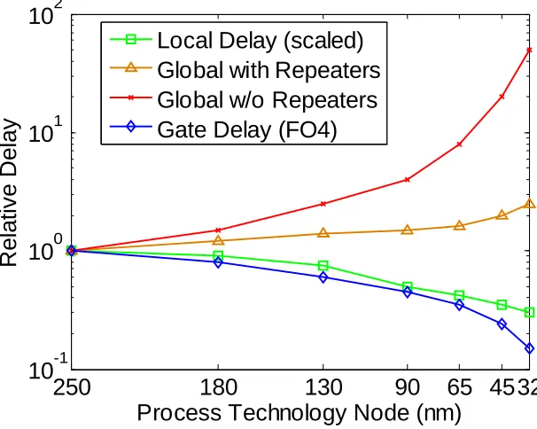
According to the ITRS roadmap 2005 [11], device delay is continuously scaled down while interconnect delay increases dramatically (Figure 1.1). Under ideal scaling, all dimensions of wires are shrunk 0.7x per generation. The wire capacitance per micron remains invariant while the resistance doubles, resulting in 1.4x increase in wire delay every generation [20]. Very large scale integrated (VLSI) circuits performance is restricted by long interconnects in deep sub-micron (DSM) technology nodes [41].
32 45 65 90 130
180 250
10-1 100 101 102
Process Technology Node (nm)
R
e
la
ti
v
e
D
e
la
y
Local Delay (scaled) Global with Repeaters Global w/o Repeaters Gate Delay (FO4)
The relationship known as Moore’s Law [68] shows that the number of transistors on a chip doubles about every two years, and the chip complexity doubles every 18 months. This law drives the device to shrink significantly. Though device size becomes smaller, chip size is continually increasing due to the growing demand for functionality and higher performance [41]. Unlike local or intermediate interconnects, global interconnects do not scale in length since they communicate signals across a chip [43]. Longer interconnects require more repeaters to be inserted to achieve timing closure and signal integrity (SI) [15]. P. Saxena et al [20] expects that if the current trends continue, 35% of the total cells will be repeaters in 45nm technology node and this number will increase to 70% in 32nm technology node. The difficulty is that interconnect behavior and the number of repeaters are hard to predict before detailed physical design. Iterative back annotation, re-synthesis, placement and routing are required, and core utilization will also become another restriction that may force design iterations.
Copper (Cu) with low-k dielectric was introduced to alleviate interconnect problems [34]. Although copper has significantly reduced interconnect delay, some researchers predict that further reduction cannot be achieved by introducing new material after 130nm technology node [15]. Low-k materials are under investigation, but are problematic due to adhesion failure [11]. There is an urgent need for innovative design technologies that can reduce interconnect wirelength.
density and the reduction of chip area. The reduced distance between blocks tends to reduce the interconnect wirelength. Studies showed that 3D integration can significantly reduce wirelength compared with its 2D counterpart [15] [33]. A shorter wirelength will reduce parasitic RC delays and lead to a smaller clock period as well as lower power dissipation.
In this work, we will concentrate on digital 3DICs. Performance trends of digital 3DICs such as timing and power were studied and proved to be attractive [32]-[33]. Tools regarding 3D floorplanning [13], 3D placement [9] and thermal optimization [5] were developed to facilitate 3D design. However, these investigations ignore non-idealities such as routing congestion and thermal impact on performance, which threaten to diminish the benefit of 3DIC. Therefore theoretical analysis of a 3DIC is not enough. We must be able to fabricate real 3D chips and perform quantitative comparisons of 3D and conventional (2D) ICs to show the real advantage of 3D integration.
1.2 Three Dimensional Integration Technologies
1.2.1 General 3D Integration Technology
before stacking to improve yield [76]. In the wafer scale integration, wafers are first stacked then cut into dies and the peripherals of the final chip are usually on top tier (in this dissertation, we give the name “tier” to each active layer and its associated metal layers). Wafers can be thinned to the scale of several microns in SOI technology or a little thicker than 10 μm in a bulk technology. Through-silicon vias are used extensively to communicate signals between different tiers. Wafer scale integration provides high-density inter-wafer interconnections and is more likely to improve performance. However, wafer scale integration usually results in higher cost because wafers are not testable before stacking.
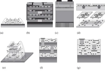
Figure 1.2 [42] illustrates seven approaches. Figure 1.2 (a), (b), and (c) can be called die scale 3D integration. (d) and (e) belong to the AC coupling. They can be either die scale or wafer scale 3D integration. (f) and (g) are wafer scale back to face 3D integration. They represent bulk and SOI 3D integration respectively. More wafer level 3D integrations like face to face, back to back or a combination of these schemes are available from different foundries such as: RTI, Ziptronix, Terrzaron, IBM, and MIT Lincoln Lab. In this thesis, we will discuss the MIT wafer level SOI 3D integration only, which will be discussed in the following section.
Figure 1.2: Illustration of 3D integration technologies. (a) wire bond; (b) microbump-3D package; (c) microbump face-to-face, 2 tier limited (d) contactless-capacitive; (e) contactless-inductive; (f) through-via bulk; and (f) through-via SOI (source [42]) 1
bumps have a much smaller pitch and can be placed anyway over the chip, and hence offers a greater vertical interconnect density. However, microbump does not significantly reduce parasitic capacitances because signals still need to be routed to the periphery before sending them back to the destination. Hence, neither wire bond nor microbump technology can achieve very high vertical interconnect density. The Contact-less technology utilizes the
1
Thanks to Dr. John Wilson for creating these figures and tables.
(a) (b) (c) (d)
electro-magnetic field of a pair of coupled capacitors, inductors, or a combination of them to transmit signals between dies or wafers. This approach eliminates the step for creating inter-tier DC connectivity and eliminates the need to route signals to the periphery. The major limitations of AC coupling is the large size of the coupling capacitance (or inductance) and the complexity of designing an analog transceiver circuit. Through-via technology seems the most promising one compared to the other 3D integration technologies. This technology offers the greatest vertical interconnect density. Wafers are bonded and then ultra-thinned. The ultra-thinning process provides better thermal removal path than die scale integration technology. All communications between tiers are transmitted by through-vias. There is no limit on number of possible tiers unless heat inside does not allow more integration. The disadvantage of this technology is relatively high cost. Since the tiers are not known to be good before assembly, the yield drops quickly as tier number increases.
Table 1.1: Comparison of 3D interconnection technologies (Source [42]) 1
Micro-bump Contact-less Through via Characteristic Wire Bond
3D Package
Face-to-face
Capacitive Inductive Bulk SOI
Assembly level Die Die Die Die/Wafer Die/Wafer Wafer Wafer Tier Limit Assembly
process
Heat Assembly process
Assembly process
Heat Heat, yield
Heat, yield Vertical Pitch
(um)
35-100 25-50 10-100 50-200 50-150 50 5
Metal layers blocked by pad
All Top 1 to 2 Top 1 to 2 Top Top 1 to 2 All, top
All, top
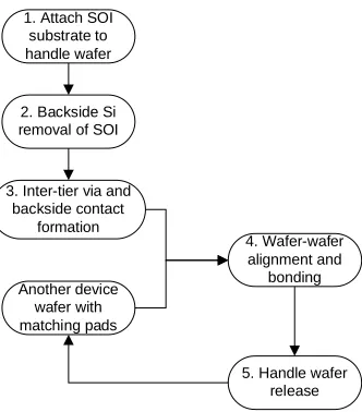
“top-down” scheme, multiple 2D circuits are fabricated and then assembled to form a 3DIC [10]. The known processing candidates are: Beam Re-crystallization, Wafer Bonding, Silicon Epitaxial Growth and Solid Phase Crystallization. The advantages and disadvantages of each processing technology are listed in Table 1.2 [15][29][30]. All the technologies except wafer bonding need to do post process that will introduce process complication and hence degrade the device performance. This degradation is hard to quantify and thus makes them less promising for 3D integration. Wafer bonding technology is the best technology currently available for 3D integration because it is the easiest to implement and is the most reliable process. Since the wafers are process separately without any interaction, we can assume same device parameters at same operation conditions. Due to the above reasons, wafer bonding is selected as the 3D integration scheme for MIT Lincoln Lab 3D process. This technology provides high vertical connectivity, similar device properties and “ System-on-a-Chip” integration [17] [21]. A process flowchart for wafer bonding technology is shown in Figure 1.3 [12][21].
Table 1.2: 3D fabrication technologies.
Beam Re-crystallization Wafer Bonding Silicon Epitaxial Growth Solid Phase Crystallization Deposit poly-sillicon and
fabricate thin film transistors (TFTs) - high temp of melting poly-sillicon
- high VT
- low carrier mobility - high-performance TFTs
Bond two or more fully processed wafers together - similar devices properties
- independent of temp - good for chip assembly with different processing technologies
- extra inter-tier vias and alignment
Epitaxially grow a single crystal Si
- high vertical connectivity
- significant degradation in quality of devices on lower layers
- difficult to implement mixed technology
Low Temp alternative to Silicon Epitaxial
1. Attach SOI substrate to handle wafer
3. Inter-tier via and backside contact
formation 2. Backside Si removal of SOI
4. Wafer-wafer alignment and
bonding Another device
wafer with matching pads
5. Handle wafer release
Figure 1.3: 3D wafer bonding process flowchart.
1.2.2 MIT Lincoln Lab 3D Integration Technology
Handle Silicon Buried Oxide
Handle Silicon Buried Oxide
Handle Silicon Buried Oxide
Ha nd le S ilic on
Bu rie d O xid e
Handle Silicon Buried Oxide
(a) (b)
(c) (d)
(e)
Figure 1.4: MITLL FDSOI wafer stacking example (source [19]). (a) Tier are fabricated with conventional IC processing; (b) Wafer2 is flipped and bond to wafer1; (c) Etching 3D
The basic sizing information is described here: design grid of this technology is 25 nm, the minimum-width poly features at 0.2 μm, the minimum metal width features at 0.25 μm
with 0.35 μm spacing for all three metal layers, the routing pitch for all metal layers features at 1 μm, the contact and vias feature at 0.4×0.4 μm2, and the 3D signal vias feature at 3×3 μm2
[19].
1.2.3 Ziptronix and Tezzaron
’
s 3D Integration Technology
Our 3DIC design flow is robust in a sense that it can adopt other wafer bonding 3D technologies besides MITLL FDSOI process. The wafer bonding technologies have similar processing steps and hence our design flow is convertible among technologies. This section will discuss two more 3D integration technologies
Unlike the SOI technology used by MIT Lincoln Lab, a bulk COMS technology would be preferred, due to the lower cost. Ziptronix and Tezzaron are the two major companies that provide 3D integration for bulk CMOS. Here we discuss the features of these technologies that differ significantly from the MITLL 3D FDSOI process.
ZiROC process is specifically suited for die scale bonding. ZiCON is a room-temperature, non-adhesive bonding that enables die scale bonding and allows known-good-die selection prior to the bonding process, minimizing potential yield losses. Standard back grinding and CMP techniques are used to thin the bonded die, and a simple, five-mask-level process is used to expose the bonding points on both die, to interconnect the two chips, and to passivate the wafer.
The 3D integration technology from Tezzaron is called “FaStack” technology [70]. Tezzaron's “FaStack” technology creates fast, dense, highly integrated 3D chips. The heart of the process is wafer scale stacking. Device circuitry is divided into sections that are built onto separate wafers using standard processing. The wafers are then post-processed for thru-silicon interconnection, creating hundreds of thousands of vertical "Super-Via" (3D inter-tier via) connectors. The wafers are aligned with a precision of 0.5 micron, then bonded, thinned, and diced into individual devices. “FaStack” devices have many advantages over their single-layer counterparts. They are much more dense and their short vertical interconnects allow them to operate at higher speeds with a lower power budget. Tezzaron claims that
“FaStack” devices match the tight integration of SoC devices while out-doing SiPs for high speed, low power budget, and tiny footprint.
bulk 3D via opening before the metal deposition to create isolation between metal via and silicon substrate.
A comparison of the three 3D integration technologies (MIT Lincoln Lab, Ziptronix, and Tezzaron) is listed in Table 1.3. Because of the lack of information, the Ziptronix data are estimated from their published figures. Symbol “~” means “approximately” because the data is based on manual measurement of a published figure. The tier thickness and 3D via size are of the same order of magnitude for all technologies. Generally speaking, the SOI process usually consumes smaller power but has poorer thermal conductivity. In this dissertation, we will focus on the MITLL process because of the detailed technology information that was available to us.
Table 1.3: 3D integration feature size comparison.
MIT Lincoln Ziptronix Tezzaron
Tier thickness 6.64 – 7.59 μm ~ 9 μm 13 μm
Bonding material SiO2 Si Si
Bonding material thickness 400 nm ~ 5 - 6 μm 5.5 μm
3D via size 3 ×3 μm2 ~ 4 ×4 μm2 2 ×2 - 4 ×4 μm2
(LEF) file that contains the design rules and technology information. The last is to update the temperature dependency parameters that will be discussed in section 3.6.
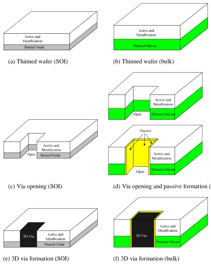
(a) Thinned wafer (SOI) (b) Thinned wafer (bulk)
Thinned Silicon Open
Passive
Active and Metallization Open Thinned Silicon
Active and Metallization
Open Buried Oxide Active and Metallization
(c) Via opening (SOI) (d) Via opening and passive formation (bulk)
(e) 3D via formation (SOI) (f) 3D via formation (bulk)
1.3 Goal of This Work
There are two major objectives of this work. The first objective aims to achieve 3DIC design automation using a combined CAD tools and algorithms. This 3DIC design flow seamlessly integrated various commercial tools with Python [38] and Tcl [39] scripts [45]. Although some potential performance is lost, it is relatively easier to explore the feasibility and advantages of 3DICs with this approach than to develop new 3D tools from scratch. This design flow provides a platform for designing 3DICs and ensures that the user can have a verified design to be fabricated. This work also demonstrates the efficiency of designing innovative 3DICs by reusing tools with a proper design flow.
leakage power [35]. This impact is especially critical for clock trees, because clock branches experiencing a temperature gradient across tiers will have significant insertion delay and transition time variation in high-performance applications. To facilitate this trade-off exploration of 3D integration, we used the automated design flow mentioned above to complete 3DIC physical design and performance analysis.
An exhaustive comparison on all circuits is the best to achieve our goal but seems impossible. We select the benchmark circuits from two different kinds of applications: low-power and high-performance. An eight-point winograd Fast Fourier Transform (FFT) is implemented to explore the trade-offs in low-power applications. 2D implementation of this FFT runs at approximately 40MHz with 810mW. An Open Risk CPU core (OR1200) with 5 SRAMs is implemented to explore the trade-offs in high-performance applications. This design runs at 60MHz with 3.3W in a 2D implementation. We selected these two designs as a starting point because they have similar speed and chip area, but significantly different power consumption and placement restrictions. These two designs are good representatives of current digital designs.
1.4 Thesis Organization
Chapter 2 outlines the current state of the art in 3DIC research and applications.
show the compatibility. Next, it approaches how the flow is assembled by explaining sub-steps of the flow and the models employed.
Chapter 4 discusses the thermal issue in 3DICs. Heat flow is the one of the most fundamental problems in 3DIC and limits the integration level a 3D system can achieve. Thermal vias are used in many 3DICs to remove heat. This chapter gives the detail of our thermal model, via pattern generation, and thermal reliability analysis.
Chapter 5 studies the performance improvement of 3DICs in the original and extended MIT Lincoln Lab FDSOI 3DIC processing technology. Extensive comparison on wire-length, timing, power, and temperature are performed. The design trade-offs among timing, power, and temperature are also explored in this chapter.
Chapter 6 gives the conclusion of this work and discusses the future direction.
Chapter 2.
Start of the Art 3DIC Tools and Progress
2.1 Summary
3D digital IC has been widely studied due to its potential to fill the gap between device scaling and interconnect scaling. The major advantages of 3DIC are the reduction of interconnect wirelength and chip area, which boost the performance of 3DIC. Figure 2.1 shows the complex interaction between the cause and effect, where the symbol “↓” means reduction. However, non-idealities will significantly cancel the advantages brought by 3DICs, and further study is required to investigate the 3D integration.
Figure 2.1: Performance boost in 3DIC.
2.2 Empirical Wirelength Reduction Analysis of 3DICs
E. F. Rent of IBM wrote two memoranda in 1960 that later developed into well known Rent’s rule. Rent’s rule was applied by researchers and designers to derive the interconnect wirelength distribution. Rent’s rule is written as (1) [15] [31], where T, N, α and p represent the number of signal inputs/outputs, the number of gates, the average number of fan-out per gate, and the degree of wiring complexity respectively. The wirelength distribution can be described by (2) [15]. I(l) means the total number of interconnects that have length less than or equal to l. Since the Rent’s rule is an empirical result obtained by observing existing designs, it is useful to apply the measured parameters of Rent’s rule to a similar architecture but would be misleading to apply the parameters to a different architecture. The system architecture becomes the key parameter that affects the accuracy of Rent’s rule. The Rent constants for various architectures are shown in Table 2.1 [73]. These constants act as guidance during our partition decision described in section 3.2.
p
N
T =α (1)
∫
=
lI
x
dx
l
I
1
(
)
)
(
(2)Table 2.1: Rent constants for various architectures.
Architecture type p α
Static Memory 0.12 6
Microprocessor 0.45 0.82
Gate Array 0.50 1.9
Chip level 0.63 1.4 High-speed Computer
The performance of a conventional system can be roughly evaluated according to the wirelength estimation based on the Rent’s rule, which is also true for 3DICs except that the estimation should be based on the 3D Rent’s rule. Extending Rent’s rule into a 3D structure with arbitrary number of active layers m, and supposing that N gates are evenly partitioned into m layers, the wirelength distribution is rewritten as (3) – (6) [32] [33], where α is related to the average fan-out which is defined by (6), V(d) is the number of connections with vertical distance of d device layers (d=1,2,···, m-1).
Horizontal wirelength distribution:
≤ ≤ − Γ < ≤ + − Γ = − − ; 2 , ) 2 ( 3 ; 1 , ) 2 2 3 ( ) ( 4 2 3 4 2 2 3 m N l m N l l m N m N l l m N l m N l l l I p p (3) 1 1 2 2 6 1 ) 3 2 )( 1 )( 1 2 ( 2 2 1 ) ( ) ) ( 1 ( 1 2 1 − − − + − − − − − + − − = Γ − − p m N p m N p p p p p p m N m N m N km p p p p
α (4)
Vertical wirelength distribution:
) ( ) 1 ( ) 1 ( 2 ) ( 1 1 2 1 d m m m N m m N kN d V p p p − − + − −
= α − − − − (5)
. . 1 . . o f o f + = α (6)
which implies a microprocessor. However, due to the arbitrary nature of value selection, the conclusion is not independent of the value of p [32]. This setup showed a maximum of 40% reduction for the longest wirelength and a 30% reduction for the average wirelength with 5 tiers at the 180 nm technology node, regardless of the technology used in their study (either SGSOI or DGSOI). They observed a dramatic improvement on circuit performance because 3D integration effectively reduced the number of long delay nets and repeaters. Compared to conventional IC circuits, the 3D integration is therefore predicted to achieve 2-3 technology generations of performance (timing) advantage. Furthermore, the DGSOI circuit can be clocked at 13%-20% higher speed while consuming 5% more power than the corresponding SGSOI circuit. However, the power delay product of DGSOI circuit is 8% lower than SGSOI circuit, which makes the DGSOI device more energy efficient.
R. Zhang et al [33] also studied the performance trend of 3DIC for the future technology generations based on a heuristic study of interconnect wirelength. Using the same simplification of the two-input NAND gate, this study showed that the total interconnect capacitance and power consumption went down first and then rose again due to a tremendous increase in vertical wirelength and the routing blockages caused by the vertical 3D vias as the number of tiers continued to increase. However, the worst case clock rate continued to speed up, even though the total capacitance increased.
3D integration was expected to significantly reduce the longest interconnects while providing a lesser advantage for average interconnects. All the m modules are divided into n tiers and the global net distribution of each tier was calculated. With a certain netlist that provided the number of N nets, placement and routing models were created to obtain the layout information. The placement information described the average dimensions of the bounding area of a net connecting a group of modules, which predicted the edge length of a net. The routing information provided a distribution of the length of a net for a given number of terminals and net-bounding area. After that, a minimum rectilinear Steiner tree (MRST) model was used to calculate the minimum total wirelength of either a single-tier or a multi-tier net. With the models created in this study, the resulting distribution showed 3D integration reduced the wirelength as the square root of the number of tier. In addition, the maximum global clock frequency is shown to increase as T2, where T is the number of tiers.
hence lead to significant performance advantages. Because of this reason, topology shown in Figure 2.2 (a) does not lead to a large reduction in interconnect length and hence less delay reduction.
Logic Memory
(a) (b)
Figure 2.2: Possible 3D partition topology: (a). Memory and logic are put on separate tiers; (b). Memory and logic are split equally to put on different tiers.
The above studies were limited in a sense that temperature was not considered one of the major limiting factors in 3DICs. Another restriction is that they did not consider the routability issue in a real design. However, the wirelength distribution investigation of their studies was the base of any theoretical analysis of 3DICs. In our case, equations (3) – (6) act as partition criterions in our partitioner (discussed in section 3.2).
2.3 Computer Aided Design (CAD) Tools
via number. They also achieved a 40% improvement on average temperature with CBA-T-fast model and a 50% improvement with CBA-T-hybrid model, which trades off between runtime and quality.
T c vc n area n wl n
cost=α⋅ _ +β⋅ _ +γ⋅ _ +η⋅ (7)
Cong’s work demonstrated that the maximum on-chip temperature can be effectively controlled through their thermal-driven floorplan algorithm. The white space or thermal via insertion can guarantee the routability issue and satisfaction of temperature constraints. However, a lack of performance analysis makes the floorplan algorithm somewhat insufficient.
a 12% reduction in maximum temperature, 1.3% reduction in average temperature and 17% reduction of thermal gradient were achieved, but there was a 5.5% increase in total wirelength compared to the same placer that does not consider thermal effects.
Partitioning and assignment to tiers
Constraint driven placement/ Simulated annealing
3D detail routing
Thermal via positioning
3D thermally-driven routing Thermally-driven 3D
placement
(a) FPGA style design flow (b) ASIC style design flow Figure 2.3: Design style for FPGA and ASIC in 3D analysis and design optimization.
thermal optimization is done, the entire circuit is detail routed as a whole. After routing, the maximum observed timing improvement approached 30%.
An automated design method was also proposed for standard cell based 3DICs [46]. In that work, the researchers developed 3D placement and global routing tools, and used MAGIC as the layout editor. The wire-length and performance characteristics of 3DIC were analyzed and shown to be attractive. However, their research showed that if heat cannot be removed from 3DIC efficiently, the performance will degrade before more tiers can be stacked.
2.4 Heat Removal
4% of the total die area could achieve two to three times reduction in effective thermal resistance.
B. Goplen et al [5] used Finite Element Analysis (FEA) to calculate temperature. To simplify their computation, they used pre-reserved regions that were uniformly placed within standard cell rows for thermal via insertion. These regions were blockages during the placement phase. After placement, thermal vias are inserted to the pre-reserved regions to reduce temperature. The entire chip was divided into sub-blocks and power was randomly generated for each block. The thermal via density of each thermal region is calculated by their FEA method. With a pre-set maximum temperature target, the thermal via density in each pre-reserved region was updated iteratively until convergence. Their experimental results showed that both temperature and thermal gradients are reduced significantly after thermal via insertion. Besides this, their results also showed that lateral thermal conductivity is much lower than vertical thermal conductivity.
Current studies showed that the use of thermal vias is a simple yet efficient method of heat removal. Thermal vias reduce both vertical and lateral temperature gradient, and hence we will use this technique in our work to remove heat as well.
2.5 3D Integration Examples
photodiode on one wafer and an analog to digital converter (ADC) on the other wafer joined by a through via. The construction of these circuits consisted of bonding and interconnecting a SOI wafer with imaging circuits and inverters to a SOI wafer with ADC circuits (illustrated in Figure 2.4). This work showed the feasibility of stacking SOI circuits to build 3DICs with dense vertical interconnects (through via). However, this study did not show a performance comparison between 3D and 2D integration.
Figure 2.4: Illustration of the 3D pixel sensor array.
functional unit. In the 3D floorplan, cache memory and function units overlap so that the load data only traveled to the center of the data cache. The same worst case path contained half as much routing distance. Since data was only traversing half of the data cache and half of the functional units, 1 clock cycle of delay was eliminated in the load execution delay. Performance improvement of the 3D iA32 microprocessor was obvious. The clock delay of store retirement was reduced by 30%, Floating Point load latency was reduced by 35%, register file read was reduced by 25%, retirement and de-allocation were reduced by 20% and other important latencies were also improved. A total of 25% pipe stages were eliminated by the 3D floorplan. In general, a 15% performance improvement was achieved by eliminating piped wire stages, reducing delay between blocks, and eliminating wire within blocks. In terms of power, a 15% total power reduction was achieved by eliminating 50% of repeaters and 50% reduction in the clock wire. The thermal problem was studied in their work. A naïve floorplan can increase heat by 10-15%. However, the thermal problem was found to be addressable at block level. In their design, the “hot” areas of the die are due to several blocks that utilize dynamic circuits to meet timing requirements. Splitting the hot blocks across two tiers could reduce internal wire delay sufficiently to allow a relaxation in the implementation of the power inefficient circuits. The power consumption of those fast hot blocks was expected to have a 50% reduction if they can be properly folded.
2.6 Unsolved Problems
Though previous researches regarding 3DICs have been proven attractive, there are still a set of unresolved problems. These problems are described below.
First, a design methodology that can assemble the tools to fabricate real 3D chips is currently not available. We developed verification models and an automated design flow to address these problems. The models and design flow are discussed in Chapter 3.
Second, 3D clock tree synthesis (CTS) is not proposed by previous research. A modern IC design will not function properly without a carefully designed clock tree. This problem becomes more critical in 3DICs because clock buffers may be operating at significant different temperatures. The synthesis and verification schemes of 3D CTS need to be developed to successfully implement the clock tree in any 3DIC.
dissipation becomes prominent. The trade-off between system performance and thermal issue must be identified.
The major features of this work are listed in Table 2.2. It tells what are provided by this work but not by previous researches. These features aims to solve the unresolved problems mentioned above.
Table 2.2: Features provided by this work.
Previous Research This Work
Conventional methodology handles 2DICs This methodology handles 3DICs Temperature range of for conventional
2DICs thermal analysis is [60°C, 110°C]
Temperature range of 3DIC thermal analysis is [0°C, 250°C]
3D tools are developed but are not applied to tape out 3DICs
This methodology is capable of taping out 3DICs
No 3D Clock tree synthesis tool or methodology has ever been reported
This methodology can handle 3D clock tree synthesis and verification
No parasitic extraction tool has been developed for 3DICs
Chapter 3.
Design and Verification Flow for 3DICs
3.1 Overview
Because 3DIC design methodologies are relatively new, there is not any standard design flow in this area. Researchers have investigated many aspects of 3D integration such as floorplanning [13], placement [9] and routing [22]. These academic tools are not verified and would require significant effort if they were used to design real 3D system. Instead of spending huge amount of time to develop and verify new tools ourselves, existing CAD tools are utilized to assemble an efficient yet reliable flow for 3DIC design. With this flow, designing 3DICs becomes feasible and their performance can be evaluated and compared to their 2D counterparts. This flow also minimizes format exchanges by using standard input/output file formats. Therefore, it will be easy to incorporate new tools into this flow as long as these new tools use standard file formats.
synthesis is a gate level netlist. The physical designers take the gate level netlist and use place and route (P&R) tools to generate layout mask patterns for fabrication while verifying the performance constraints and design rules are met [7]. The flow was developed to help designers to avoid excessive interaction between different groups by clearly defining group tasks.
(a) 2DIC design flow (b) NCSU 3DIC design flow
Figure 3.1: Comparison between conventional 2DIC design flow and our 3DIC design flow.
conventional flow, too, except that there are more design constraints. Another difference is that a thermal check is implemented to verify the performance and reliability of 3DICs.
PowerCompiler from Synopsys and switching-activity annotations from Verilog simulation. Lastly, an electro-thermal coupling analysis was executed to determine the actual performance and determine if any design iteration will be invoked based on weather or not there exists any performance violation. The final flow supports place-and-route for up to 10 tiers and 7 layers of metal per tier.
Synthesis Result (normal netlsit)
Partition (use metis)
Floorplan
Thermal Design
Placement
Clock Tree Synthesis, Thermal
refinement
Routing (global and detail)
Update Timing & Power Timing & Power
Simulation
Thermal Simulation
Converge? No
Yes
Timing Check
Done Pass Fail
Figure 3.2: 3DIC physical design flow.
DRC and LVS check are split from the automatic design flow because excessive manual fixes are required whenever an error occurs, which makes it hard to be automated. In the following sections of this chapter, each design step will be discussed in detail.
3.2 Circuit Partitioning
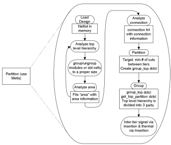
Figure 3.3: Partition flow.
analyze top level hierarchy; step3: group/ungroup modules or standard cells; step4: analyze module area; step5: analyze connection; step6: circuit partition; step7: grouping different modules into partitions; and step8: insert inter-tier signal via and thermal via.
Once the design is loaded into memory, this partitioner will analyze the top level hierarchy. The purpose of step2, step3, and step4 is to create groups of cells in the netlist that have similar area and can there be floorplanned conveniently. Step2 analyzes the top level module size and sparse standard cell count. Huge module should be avoided because it will destroy the balance of cell area on different tiers, while large number of sparse standard cells significantly increases runtime. Hence, a grouping and/or ungrouping is employed in step3. Grouping is a manual process of combining some standard cells and ungrouping other units of hierarchy until all modules in the top-level of hierarchy have similar area. As a rule of thumb, the difference in area between the largest and smallest modules should be around 5. Exception occurs only if the original top-level hierarchy contains some very small modules. Iterations between step2 and step4 could occur until we got a proper top level hierarchy. After the proper hierarchy is obtained, area is annotated to each module and this information is saved as a text file with name
area information is used to balance the cell area in different tiers and the connection information is used to minimize the cuts between tiers. The partitioner calls k-METIS to create an N-way partition with minimized cuts and analyzes k-METIS’ output. Then a file named
“group_top.dctcl” is created (step6), which contains Design Compiler commands to create the necessary groups. The tier that consumes the most power should be assigned closer to the heat sink and subsequent tiers should be ordered from hottest to coolest, going away from the heat sink. File “group_top.dctcl” is executed in step7. Also in this step, the Tcl file
“get_top_parititon.dctcl” is executed to traverse all the sparse standard cells and analyzes connections of their inputs and outputs. If a cell is connected to a module or a standard cell on certain tier, this standard cell is assigned to that tier too. If a cell is connected to multiple tiers, then the cell will be assigned to the tier where its output pin is connected to.
When the partition is done, an inter-tier signal via insertion procedure is invoked. The partitioner analyzes all nets in the top level hierarchy. Any net that spans more than one tier (group) is broken down and inter-tier signal vias are inserted to connect its branches on different tiers. Each branch is assigned a suffix with “_tier#”, where # represents the tier number or tier name. The original nets are removed from the netlist. If the net connects multiple tiers or goes through certain intermediate tiers without any connection, through vias will be inserted. Thermal via insertion follows the signal via insertion. Currently, the number of thermal vias on each tier is predefined and identical for all tiers. After all vias are inserted, tier specific netlists are generated.
circuits used in this study are a microprocessor and a logic circuit. According to Table 2.1 in section 2.2, we set the exponential rent’s constant p to 0.45 and 0.5 respectively, while α is set to 0.82 and 1.9 respectively. The total wirelength is analyzed with different gate count and tier count and the results are plotted in Figure 3.5. The left part of Figure 3.4 shows how the total wirelength in a microprocessor changes as gate count varies from 100 to 1000000 with different number of tiers, while the right part of Figure 3.4 enlarges the region where gate count is between 1000 and 5000. Figure 3.5 shows the results for a random logic. As can be seen from the figure, for both design types with the provided parameters, gate count equals 5000 is the threshold. Any module with less than 5000 gates does not worth partition because the wirelength improvement is very small. The cell area of a 2-input NAND gate is 48 μm2 in our library, so we consider any module smaller than 5000×48μm2 = 240000μm2 does not deserve partition too. Finally, we conclude that 5000 cells or 240000μm2cell area, whichever comes first, is the partition threshold for a module.
Microprocessor 1 100 10000 1000000 100000000
100 1000 10000 100000 1000000 Gate Count W ir e le n g th ( u n it l en g th ) 1 tier 3 tiers 7 tiers 10 tiers Microprocessor 0 5000 10000 15000 20000
100 1000 10000 100000
Gate Count W ir e le n g th ( u n it l en g th ) 1 tier 3 tiers 7 tiers 10 tiers
Random Logic 1 100 10000 1000000 100000000
100 1000 10000 100000 1000000 Gate Count W ir el e g n th ( u n it l e n g th ) 1 tier 3 tiers 7 tiers 10 tiers Random Logic 0 10000 20000 30000 40000 50000
100 1000 10000 100000
Gate Count W ir el e n g th ( u n it l e n g th ) 1 tier 3 tiers 7 tiers 10 tiers
Figure 3.5: Total wirelength vs. gate count at different tier count for a random logic.
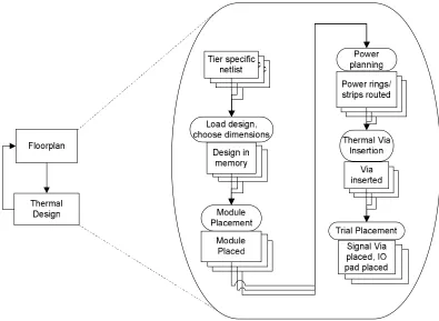
3.3 Floorplanning and Thermal Design
Figure 3.6: Floorplan and thermal design.
thermal vias can be inserted according to the local power density. More detail of thermal via planning is discussed in section 4.2
Since IO pads are assumed to exist only on the top tier, several hundred signal vias are used to connect power/ground rails on different tiers, which provide better power distribution and hence reduce IR drop. In this flow, power/ground signal vias are placed along the location of vertical power/ground stripes to save area.
The last step in this flow is signal via and IO pad placement. We will first perform a trial placement on each tier to get the appropriate location for each inter-tier signal via and IO pad. IO pads are placed at core boundaries and a trial placement can determine the locations for most signal pads, though the location of the signal pads are adjustable in later steps. The pad pitch of the MIT technology we used is 100 μm. The determination of locations for inter-tier signal vias is more difficult. If we consider the three-tier MIT process as an example, we use equations (8)
– (11) to determine the locations of those inter-tier vias. These equations basically set the new via location on each tier to be the centroid of the previous two locations. Inter-tier vias are then placed to these new locations.
For VIA_AC: s connection TierC s connection TierA coordinate TierB s connection TierC coordinate TierA s connection TierA location new _ _ _ _ _ _ _ + × + × = (10) For VIA_ABC: s connection TierC s connection TierB s connection TierA coordinate TierC s connection TierC coordinate TierB s connection TierB coordinate TierA s connection TierA location new _ _ _ ) _ _ _ _ _ _ ( _ + + × + × + × = (11)
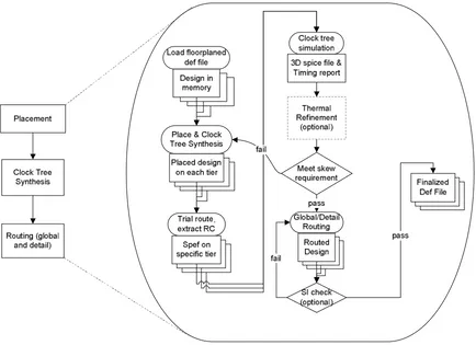
3.4 Placement, CTS, and Route
Directly following the result of floorplanning, the Place & Route (P&R) sub-flow will be invoked. The entire P&R flow is show in Figure 3.7. In this sub-flow, we will do placement, Clock Tree Synthesis (CTS), routing and tier specific Signal Integrity (SI) checks. Besides the normal P&R steps, a thermal refinement (to modify the locations of thermal vias) step during the analysis later in the flow is defined as an option for designers if they identify any thermal violation during the analysis later in the flow.
capacitors and transistors. A SPICE simulation is invoked when the parasitic merge is done. Then we calculate clock skew in the form of (12). If skew meets our specification, we go to next step, otherwise we will load the placed design and change CTS specs to do another synthesis until the skew meets the specification.
Figure 3.7: Place, clock tree synthesis, and routing.
delay insertion
Minimum delay
insertion Maximum
skew= _ _ − _ _ (12)
and temperature. In this case, thermal via cells are moved from the regions with low temperatures to the hot spots to make the temperature profile more uniform. Since the thermal conductivity of thermal via (Tungsten) is two orders of magnitude larger than the Silicon-Dioxide, a slight increase of thermal via significantly improves the equivalent thermal conductivity in the hot region and hence reduces the temperature a lot. Besides, delay is also temperature dependent and we may have clock skew violation if the clock buffers are operating at significant different temperatures. If such violations are identified during analysis, thermal vias have to be moved closer to clock buffers operating at higher temperatures to bring heat away. On the other hand, stacking of clock buffers should be avoided if possible. However, this process is optional because a designer may find the temperatures at hot spots are below threshold so that no further action is required.
3.4.1 Parasitics of 3D Inter-tier Via
(a). VIA_AB isolated (b). VIA_AB Shield
Figure 3.8: Inter-tier via modeled in Q3D.2
The parasitics of a 3D via is a very important parameter for both clock tree verification and final performance verification. Because this data was not provided by the foundry, an electromagnetic field solver Q3D [50] was used to simulate the parasitic data for these vias by solving capacitance matrices. Shown in Figure 3.8 [49], two configurations of a 3D via connecting tier A (bottom tier) and tier B (one tier up) are simulated to find the parasitic capacitance bounds. Figure 3.8 (a) shows the isolated case that there is no metal around the 3D via, which gives the lower bound of the parasitic capacitance. Figure 3.8 (b) shows the shielded
2
case, in which the 3D via was surrounded by all possible metal layers with minimum distance, which gives the upper bound.
Though parasitic resistance seems identical for different 3D vias and shielding, Q3D
simulations of MIT Lincoln Lab technology show a slight difference on parasitic capacitance of via AB and via BC. The parasitic data is listed in Table 3.1. The parasitic capacitance of shielded 3D via is roughly equivalent to a 20 μm minimum width minimum distance shielded metal2 wire. The resistance is very small when compared with either a 20 μm metal2 wire or a normal via (4Ω), which makes it negligible during later parasitic extraction and merging. In the MIT 3D technology, via AC (and ABC) constitutes of one via AB and on via BC.
Table 3.1: 3D via parasitic.3
Capacitance Isolated Tier(s)
Handle-silicon only
With back-metal
Shielded Resistance
AB 0.82 fF 0.99 fF 4.34 fF 0.115 Ω
Inter-Tier
Via BC 0.89 fF 1.01 fF 4.15 fF 0.115 Ω
A 1.01 fF 3.69 fF 4.43 fF 6.4 Ω
B 0.95 fF 3.27 fF 4.42 fF 6.4 Ω
Metal 2 (20 μm)
C 0.89 fF 3.66 fF 4.41 fF 6.4 Ω
3.4.2 3D Clock Tree Insertion
We have investigated two clock tree insertion schemes within this flow. They are illustrated in Figure 3.9. The scheme shown in Figure 3.9 (a) is defined as “Root-Pin CTS” because the clock tree on each tier is inserted from boundary pins that are aligned to the same
3
X-Y position on each tier. 3D vias are later inserted just outside the boundary to connect these nets. This synthesis scheme is a straightforward extension of a conventional 2DIC CTS. However, if we use this scheme in 3DIC design, we find the clock skew is very hard to control, because the loads on each branch of the clock tree are difficult to balance. According to the Elmore model, the clock-to-first-level-buffer delay and slew rate of the nodes N1 ~ Nn in Figure 3.9 varies significantly tier-to-tier due to the complex RC topology, especially when tier number is large. So another scheme defined as “Root-Cell CTS”, which is shown in Figure 3.9 (b), is developed to reduce the RC complexity at clock pad output. Rather than use the boundary pin as the clock source, Root-Cell CTS creates a clock source buffer on each tier and aligns them to the same X-Y position on each tier, somewhere close to the off-chip clock pad. Then tier specific clock source buffer acts as the source of the clock tree. The parasitics on the first level of the clock tree are more predictable with this method, so the delays and slew rate from clock pad to node N1 ~ Nn are more controllable in this scheme. To insert the clock tree under the “Root-Cell CTS” scheme, one set of clock tree constraints is created for each tier. Clock trees are inserted and verified respectively and will be joined for final verification if clock trees on each tier have similar insertion delay and transition time.
As shown in Figure 3.10, the parasitics of both CTS schemes are demonstrated. In the Root-pin CTS scheme, “RC parasitics tier n” represents the RC network between a 3D via and the first level clock buffers inputs. These parasitics are subject to change during different iterations of the design flow and are very difficult to control. Therefore, the delay at node N1 ~
constant as long as the number of tiers is determined and hence the delay at node N1 ~ Nn remains unchanged. Then the 3D CTS problem is reduced to a 2D CTS problem that is well defined in any commercial tool.
A brief performance comparison between these two clock tree insertion schemes is listed in Table 3.2. The two benchmark circuits are implemented in the original MIT Lincoln Lab process (three tiers, three metal layers) in both 2D and 3D integration using manual tweaking to help reduce the clock skew. As can be seen from the table, the clock skew is significantly reduced with Root-Cell CTS by paying a tiny price of power. In this experiment, the same skew target 400ps was set to each CTS scheme. The final skew values were obtained from the CTS verification flow after detail route.
(a) (b)
Figure 3.9: Clock tree insertion schemes. (a) Root-Pin CTS, clock tree is inserted on all tiers simultaneously; and (b) Root-Cell CTS, clock trees are inserted on different tier respectively
RC parasitics tier n
RC parasitics tier n-1
RC parasitics tier 2
RC parasitics tier 1
3D Via Parasitic Model Clock
Pad
N1
N2
Nn-1
Nn
(a) (b)
Figure 3.10: Clock tree parasitics. (a) Root-Pin CTS; and (b) Root-Cell CTS. Table 3.2: Performance Comparison between Root-Pin CTS and Root-Cell CTS
2D CTS Root-Pin CTS Root-Cell CTS
Clock skew Power Clock skew Power Clock skew Power
FFT 489 ps 233 mW 446 ps 195 mW 196 ps 202 mW
ORPSOC 532 ps 794 mW 457 ps 467 mW 180 ps 483 mW
3.5 Timing and Power Simulation at Nominal Temeperature
power/material density report file will be generated for electro-thermal delay-power coupling analysis4.
Figure 3.11: Timing and power simulation flow with nominal temperature.
First, the tier specific SPEF files are merged to provide parasitic data for the 3D design5. The detailed SPEF merge methodology is described in [49]. The parasitics of the detail routed 3D clock tree will be extracted for a SPICE simulation to update final insertion delay and transition time. The clock skew is calculated with (12) shown in section 3.4. PrimeTime reads the top-level verilog netlist, final clock skew, and merged SPEF file, then reports critical path delay and checks for hold violation. The hold time check is most critical for the success of any digital circuit because hold time violation will cause the chip to fail at any clock frequency.
4
Thanks to Samson Melamed for creating the density report file format. 5
PrimePower [64]6 takes the inputs of PrimeTime6 along with a Value Change Dump (VCD) file7. It analyzes the circuit and generates a power report for each cell. This power report is analyzed along with the tier specific DEF files to generate a file containing power/material density information4.
The power/material density report contains following information in sequence: tier-count, row number, column number, metal density on north edge, metal density on south edge, metal density on east edge, metal density on west edge, thermal via density in current region (a region is defined as a rectangular or square block with certain area on the chip) connected to upper tier, thermal via density in current region connected to lower tier, average dynamic power, and average leakage power. Currently, only metal, inter-tier vias (both signal and thermal), and silicon dioxide are considered for heat conduction.
A later power estimation flow adopts 10 tiers uses a different approach. To being, a forward annotation Switching Activity Interchange Format (SAIF) file is created in Design
Compiler. To write a forward annotation SAIF file in design compiler, the RTL description of
the design must first be loaded and linked. Then the “rtl2saif” command is used to interpret the design and finally write a forward annotation SAIF file [47]. When the SAIF file and parasitics are obtained for the design, Design Compiler is used to estimate the power consumption.
3.6 Electro-Thermal Power-Delay Analysis
The actual performance of a 3DIC may be significantly different from the value obtained from nominal temperature simulation. Because the temperature, delay, and power are
6
In the extended technology, Design Compiler is used instead of PrimePower and PrimeTime 7
![Figure 1.4: MITLL FDSOI wafer stacking example (source [19]). (a) Tier are fabricated](https://thumb-us.123doks.com/thumbv2/123dok_us/1326969.1165604/22.612.110.529.84.593/figure-mitll-fdsoi-wafer-stacking-example-source-fabricated.webp)