ISSN(Online): 2320-9801
ISSN (Print) : 2320-9798
I
nternational
J
ournal of
I
nnovative
R
esearch in
C
omputer
and
C
ommunication
E
ngineering
(An ISO 3297: 2007 Certified Organization)
Vol. 4, Issue 3, March 2016
A Concurrent BIST Architecture for Testing
Integrated Circuits with Modified SRAM
Cells
C.Catherine Reni 1, C.Naveen Arockia Raj 2, M.Sivakumar 3
P.G. Student, Department of ECE, Adhiyamaan College of Engineering, M.G.R Nagar, Hosur, India1
U.G. Student, Department of ECE, Adhiyamaan College of Engineering, M.G.R Nagar, Hosur, India2
Associate Professor, Department of ECE, Adhiyamaan College of Engineering, M.G.R Nagar, Hosur, India3
ABSTRACT: Integrated circuits are tested using BIST technique which provides self-testability of the circuit and
avoids the requirement of external testing equipment. This method achieves simultaneous testing of the circuits under online mode. The aim of proposed project is to design the active test set generator and comparator circuit and logic module with SRAM cells to store input test vectors and to reduce the switching activity with reduced testing time and Concurrent Test Latency(CTL). The proposed scheme is suitable for all types of IC’s and achievement of fault coverage is high.
KEYWORDS:Built-In-Self Test, Active Test Set Generator and Comparator Circuit, Very Large Scale Integrated
Circuits, Static Random Access Memory.
I.INTRODUCTION
Testing of VLSI circuits use BIST techniques,which are classified into offline and online mode of testing. In online mode the circuit operates in parallel and to make testing process faster than the scan based testing method. BIST technique provides high fault coverage. TG is a test pattern generator circuit which is designed to generate random test patterns to test faults in integrated circuits and test patterns are moved to MUX with the help of selection line the MUX passes the input vector to the circuit under test (CUT) and AGC is a active test set generator and comparator circuit simultaneously passes the active test set to response verifier (RV) and CUT also passes the output response to the response verifier which compares both the vectors and if both the vectors match then it indicates that hit of vector occurs if not then the IC is a faulty one.
Logic module generates the test patterns to detect the faults and indicate the result to the outputs. As the test pattern generator is a circuit area is limited. Therefore storing and then generating test patterns by ATPG on the circuit under test using the hardware test pattern generator is not possible. The main aim of the register design is to have low area to generate many different patterns (from 0 to 2n ).
Logic module has the following cases:
1) reset of the module
2) hit of a vector
3) tge operation
ISSN(Online): 2320-9801
ISSN (Print) : 2320-9798
I
nternational
J
ournal of
I
nnovative
R
esearch in
C
omputer
and
C
ommunication
E
ngineering
(An ISO 3297: 2007 Certified Organization)
Vol. 4, Issue 3, March 2016
When all the cells value are equal to 1 then the value of the w-stage counter is all 1. The activation of the rve signal to the counter to overflow and in the next clock cycle through the unit flop delay the tge signal is enabled and all the cells value to all the outputs of the decoder are enabled and are set to zero.
II.RELATIVE WORK
1.Structural on-line self-test was performed to detect permanent faults and avoid their accumulation in the circuit[1]. This method improves concurrent BIST techniques based on a deterministic active test set. Here, the test patterns for testing are especially generated with a specified number of smaller bits . This results in very low test latency, which reduces the fault accumulation. Experiments with a large number of circuits show that the hardware overhead is comparatively lower than the overhead for previously used testing methods. Dormant faults and subsequent fault accumulation can also decrease the system reliability and also require additional on-line testing techniques.
2.This method of modular CIS sub-array is proposed with new account and to control scheme. It needs only one micro-bump per sub-array and instead of per-pixel or per-column and to release the design rule restriction of the 3D stacking process in the testing of VLSI circuits. The proposed structure with in-pixel two-dimensional (2D) decoding function makes high spatial resolution, without affecting the frame rate of testing process[7]. A BIST circuit is also to filter out errored CIS layer before chip stacking to improve the yield performance of the final 3D integrated IC's, without adding an extra transistor in the pixel of the circuit. The proposed modular sub-array is designed with expected value of 100 fps at multi stage mega imaging in high-speed HDTV camera applications in VLSI domain.
3.Concurrent Error Detection (CED) in a popular method of asynchronous controllers as Burst-Mode machines[3]. These clock-less circuits, including the use of redundant bits to check hazard-free operation, and to explain how they limit the applicability of traditional CED methods, such as duplication in the testing method. This method demonstrates how duplication can be enhanced to resolve the limitations through additional hardware for comparing synchronization and detection of error-induced hazards, which spoils the interaction of the circuit with its environment. At last, function to avoid the need for hazard free error detection circuitry and hazard-free implementation of the duplicate was introduced. Many types of CED methods developed for synchronous controllers, their parts with asynchronous counterparts are intrinsically different, reduces the effectiveness of the previous methods.
III. PROPOSED WORK
The input vector monitoring concurrent BIST scheme, which monitors a set of vectors called window of vectors reaching the circuit inputs during normal operation, and the CAM memory cells to store the relative locations of the vectors. The proposed scheme is based on the hardware overhead of the circuit and the concurrent test latency (CTL) which shows to perform considerably better than previously proposed schemes with respect to the hardware overhead and CTL tradeoff.
ISSN(Online): 2320-9801
ISSN (Print) : 2320-9798
I
nternational
J
ournal of
I
nnovative
R
esearch in
C
omputer
and
C
ommunication
E
ngineering
(An ISO 3297: 2007 Certified Organization)
Vol. 4, Issue 3, March 2016
Let us consider a CUT with m inputs. The number of the possible input vectors for this CUT is N = 2m. The proposed scheme is based on the idea of monitoring test patterns, whose size is W, with W= 2w, where w is an integer number w <m. The test vectors belonging to the window of vector are monitored, and if a vector performs a hit, called hit of a vector and the RV is enabled. The number of test patterns which we want to monitor in parallel is K, the number of the words of the RAM utilize reasons, K is chosen to be a power of 2, i.e. K = 2k. The bits of the input vector are separated into two distinct sets comprising wand k bits, respectively, such that w + k = m.
A. Hardware test pattern generator
This unit generates the test patterns required to detect the faults in IC and to propagate the effect to the outputs. As the test pattern generator is a circuit (not Equipment) and it is area is limited. So storing and then generating test patterns by ATPG algorithms on the CUT and using the hardware test pattern generator is not possible. Instead, the test pattern generator is basically a type of register which generates the random patterns which act as test patterns.
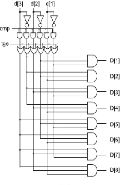
B.Modified Decoder
The design of the m_dec module for w = 3 and operates as follows. When test generator enable (tgen) is enabled, all outputs of the decoder are equal to 1. When comparator (cmp) is disabled (and tgen is not enabled) all outputs are disabled. When tgen is disabled and cmp is enabled, the unit operates as a normal decoding structure. The architecture of the proposed scheme for the specific case n = 5 bits, k = 2 bits, and w = 3bits.
ISSN(Online): 2320-9801
ISSN (Print) : 2320-9798
I
nternational
J
ournal of
I
nnovative
R
esearch in
C
omputer
and
C
ommunication
E
ngineering
(An ISO 3297: 2007 Certified Organization)
Vol. 4, Issue 3, March 2016
C. Comparator
A comparator is a circuit compares a signal on one input of an op-amp with a known voltage called the reference voltage on the other input. Comparator is an open loop op-amp with two analog inputs (differential input ) and one digital output (signal ended output). Comparator is a combinatorial circuit thatcompares 2 numbers, A and B, and gives their relative magnitudes. The circuit, for comparing 2 n-Bit numbers, has 2n inputs. The logic style used in logic gates basically influences the speed, size, power dissipation, and the wiring complexity of a circuit under test.
D.CUT
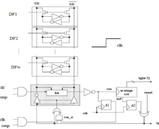
During normal mode, the inputs to the CUT are driven from the normal inputs. The n inputs are also driven to the CBU as follows: the w lower order inputs are driven to the inputs of the decoder; the K higher order inputs are driven to the inputs of the comparator. When a vector belonging to the current window reaches the inputs of the CUT, the comparator is enabled and one of the outputs of the decoder is enabled. During the first half of the clock cycle (clk and cmp are enabled) the addressed cell is read; because the read value is zero, the w-stage counter is triggered through the NOT gate with output the response verifier enable (rve) signal.
IV.MODIFIED SRAM CELLS
SRAM is a type of semiconductor memory cell that uses bistable latching circuit to store each bit in the memory cell. Two types of SRAM cells are there one is static (SRAM) and another dynamic (DRAM).The dynamic RAM (DRAM) must be periodically refreshed. SRAM exhibits a datastability, but it is volatile in the conventional sense amplifier and that data is automatically lost when the memory cell is turned off. The power consumption of SRAM varies widely depending on how frequently it is used and it is termed as power-hungry as DRAM, when it is used at high frequencies, and some IC's can consume many watts at full bandwidth of power. Static RAM in applications such as moderately clocked microprocessors, consumes little power and can have a less power consumption of a few micro-watts.
ISSN(Online): 2320-9801
ISSN (Print) : 2320-9798
I
nternational
J
ournal of
I
nnovative
R
esearch in
C
omputer
and
C
ommunication
E
ngineering
(An ISO 3297: 2007 Certified Organization)
Vol. 4, Issue 3, March 2016
A 10T SRAM cell consists of 10 transistors from which four are pull-up transistors (PUS1, PUS2, PUT1 and PUT2), four are pull down transistors (PDS1, PDS2, PDT1 and PDT2) and two are access transistors (PQR and PXY). The two pulldown transistors i.e. PDS1 and PDT1 are connected to VGND. This VGND signal is connected to gnd during the read_operation else to VDD. o The access transistors are connected to pseudo nodes (PQ and PQb i.e. nodes between two pull-up transistors)but not to the storage nodes (i.e. Q and Qb). Due to this operation, the storage nodes are changed from the BLs and therefore during the read_operation of the circuit ,the current flows through the storage nodes and hence maintain the read mode stable. Wheras in case of the write_operation, the VGND is connected to VDD and any one of the bit-lines e.g. BL is in gnd. Suppose the node Q is storing ‘1’ value and node Qb is storing ‘0’ value. When a high supply voltage is supplied, the node Q value is pulled down to ‘0’ value and then due to discharging through the access transistor the pull-up transistor i.e. PGL and PUL2.
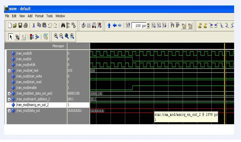
V. SIMULATION RESULT
The proposed Architecture circuits have been simulated using Xilinx .14.5 tool.XilinxISE(Integrated Software Environment) is a software tool produced by Xilinx for synthesis and analysisof HDL designs, enabling the developer to synthesize (compile) their designs, perform timing analysis, examineRTL diagrams,simulate a design's reaction to different stimuli, and configure the target device withthe programmer.
Fig. 4. Simulation output
VI. CONCLUSION AND FUTURE WORK
ISSN(Online): 2320-9801
ISSN (Print) : 2320-9798
I
nternational
J
ournal of
I
nnovative
R
esearch in
C
omputer
and
C
ommunication
E
ngineering
(An ISO 3297: 2007 Certified Organization)
Vol. 4, Issue 3, March 2016
REFERENCES
1. Ioannis,CostasEfstathiou “Concurrent self test with partially specified patterns for low test latency and overhead,” IEEE Transaction on very large Scale integration system, vol. 22, no.7, July 2014.
2.S. Almukhaizim and Y. Makris,“Test challenges for 3D integrated circuits using ring oscillators,”IEEE Trans. Comput., vol. 56,no. 6, pp. 785–798, Jun. 2007.
3. I. Voyiatzis and C. Halatsis, “Test pin methodology, architecture and circuits for testing in 3D stacking ic systems,” IEEE Trans.Dependable Secure Comput.,vol. 2, no. 2, pp. 150–156, Apr. 2005.
4. R. Sharma and K. K. Saluja., “Theory, analysis and implementation of an on-line BIST technique,” vol. 34, no. 9, May 1993.
5. K. K. Saluja, R. Sharma, and C. R. Kime, “Concurrent comparative built-in testing of digital circuits,” Dept. Electr.Comput.Eng., Univ. Wisconsin, Madison, WI, USA, Tech. Rep. ECE-8711, 1986.
6. J. Rajski and J. Tyszer, “Test responses compaction in accumulators with rotate carry adders,” IEEE Trans. Comput.Aided Design Integr. Circuits Syst., vol. 12, no. 4, pp. 531–539, Apr. 1993.