Design and Implementation of Area Efficient BIST
Based Vedic and Wallace Tree Multipliers on
FPGA
Sandugari Bhargavi1, Sapati Upendar2 1, 2
Electronics and Communication Engineering Department (VLSISD), JNTUH University
Abstract:The development of low power design of any configurable hardware designs is the increasing applications of integrated
circuits in everyday useful electronic gadgets. The modern circuit designers have been looking for the two important parameters namely high speed and low power. The multiplier is an operational unit of processing element in digital signal processing applications .The most important design of DSP is multiplier design for complex data processing .The performance of multipliers is among the efficiency improvement factor of any digital hardware design. Another feature of hardware circuits is self-testing ability. This type of testing provides reliability to the hardware mainly in case of configurable hardware applications BIST helps to decrease the testing time of hardware function authenticity and it meets the requirements such as high reliability, low repair cycle time. The main objective is to decrease the power dissipation without affecting fault covering. However thereby reduces the dependence external ATE. The important feature of hardware designs is Built-in-Self Test (BIST) feature helps in quick diagnosis of the hardware circuit functional authenticity. This paper presents a BIST based implementation and general ATPG testing of Vedic and Wallace tree multipliers. The proposed design is realized using Xilinx Tool (14.7) using Verilog. A low power Test Pattern Generator (TPG) is involved in the design for self-test circuit realization.
Keywords: Built-In-Self-Test, Test Pattern Generator, Linear Feedback Shift Register, Xilinx Tool 14.7 version.
I. INTRODUCTION
The main important factor in any circuit or device is testing. Testing can be done internally and externally. Externally the testing can be performed manually but there is no such option for the internal testing. So the component BIST is involved to the circuit internally by itself. Now a days, integrated circuits contains some millions of transistors with high circuit density. The costs and chip area overhead becoming more essential to minimize these various testing schemes that offers high coverage of faults. The present integrated circuits are tested by using various design for testability (DFT) techniques, this techniques are generally based on the concept of making the circuits controllable and also more observable [1].
Nowadays, a configurable hardware structure performance can be determined using its operational speed and also power. Field Programmable Gate Array (FPGA) is among the configurable devices provides with the desired promising power and speed based hardware circuit performance. In FPGA the operation flow is based on the internal path switching of current through a combination of different hardware resource structures. A hardware based optimization of any circuit can be achieved by the modification of the operational design architecture. A low power circuit offers the advantages like device portability, very long battery life, better performance criteria, etc. For modern digital applications a very high speed processor with very low power requirement design is the minimum basic criteria. The important design of any digital signal processors is a multiplier design. The multiplier is used in almost all high complex data processing applications. The self-testing feature is a feature that requires in the hardware for self diagnosis or self-testing. This feature helps the integrated configurable circuit hardware to test by itself and also in case of hardware fault, this feature helps to re-locate the resources of hardware within the integrated circuit. In the self-test operation, hardware is tested for its functional output with the help of a supplementary hardware.
II. BIST BLOCK DIAGRAM
Fig. 1 Block diagram of BIST
So the component BIST is involved to the circuit internally by itself. The term Built-in-self-test is a technique in which it integrates the functionality of an automatic test system on to a chip. In order to solve the testing problems of any complex VLSI circuits, BIST techniques has been used widely and studied extensively. BSIT not only tests by itself but also helps to re-locate the resources of hardware present in integrated circuits, in case of any faults in the hardware [2].
It is one of the designs for testability (DFT) techniques, in this the test application as well as test generation is done through the built in hardware features. The Basic BIST block diagram contains three hardware blocks, namely Test pattern generator, Output response analyzer, Test controller.
A test pattern generator is used to generate the test patterns for the circuit under test. We can either use a counter or a ROM which contains stored patterns or an LFSR .LFSR contains D-flip flops and exclusive OR logic and LFSR are two types, external LFSR and internal LFSR .in external type XOR gates are placed outside the shift path and in internal type XOR gates are placed in between the flip flops [10].Output response analyzer is used to analyze and compare with the stored patterns responses and here LFSR is used as a signature analyzer. It is used to analyze the test responses in order to determine the CUT correctness. A test controller is needed to activate and also to control the test and to analyze the test responses from the circuit. However many test related functions can be examined through a test controller.
In the normal operation mode it performs the defined logic operation on DATA Input. When it is operated in Self-Test mode, a random sequence of data is generated by Test pattern Generator using control signal by BIST Controller. This test sequence is operated by Logic Circuit and the generated output of the logic operation is compared with the actual output. The comparator output indicates logic high if the output of the logic operation against the test inputs does not match with the actual output. This condition indicates a fault in the logic circuit hardware. In such cases a configurable hardware re-locates the circuit resources within the integrated circuit to avoid the faulty hardware.
Related to this low power design of BIST based logic circuit for hardware design applications many architectural modifications are proposed by many researchers and scholars in their work. A low power test pattern generator design is proposed using a low-power Linear Feedback Shift Register for BIST structures [2]. This design follows the approach based up on single input change pattern generated by a gray code converter and a counter in order to decrease the switching activity. FPGA Implementation of an LFSR based Pseudorandom Pattern Generator for MEMS Testing [3]. This design has many characteristics such as it consumes less power, speed is very high and it is especially suited when uniform distribution random numbers are required such as in processors. A Low Power linear feedback shift register based low power test pattern generator design [4].
In this paper, in order to avoid the repetitive pattern the reseeding method is used a random number is generated by using WELL method first and its performance was analyzed. For very high speed applications using FPGA devices many researches performed on logical operational units. A review on Vedic Mathematics for digital signal processing operations [10]. This is based on Vedic mathematics which deals with exhaustive review of literature. And also in this paper, an improved efficiency of Vedic multiplier is proved over conventional multiplier. An FPGA based implementation of high speed 16-bit Vedic multiplier using LFSR [11]. This paper deals with the implementation of 16-bit Vedic multiplier which is enhanced with automatic insertion of all input possible combinations and propagation delay. The test pattern generator is an important major component of hardware BIST design. Many BIST application circuits are simulated and proposed by many scholars to propose speed and power optimized designs based on implementation of FPGA. FPGA implementation of BIST enabled UART for Real Time Interface Applications [1]. This paper describes about the UART functional verification of various blocks. A concurrent BIST architecture for online input vector monitoring design [12]. It describes about the idea of monitoring a set of vectors reaching the inputs of circuits at the time of normal operation and uses SRAM like architecture which is used to store the relative locations of the vectors that are reaching the inputs of the circuit. A BIST enabled I2C protocol design implementation on FPGA [13], it describes the design that enables a common hardware self test interface protocol for very high speed communication devices. The main important requirement of the today’s hardware designs is implementation of low power circuit of BIST based logic circuits. for low power implementation, A multiplier with two 4-bit inputs is taken as a test design on FPGA with self-test capability. The self-test feature is also included using a low-power TPG design. a modified architecture is used for the design of test patterns by reducing the number of sequential component as compared to the conventional design components.
III. MULTIPLIER DESIGN AND TEST PATTERN GENERATOR
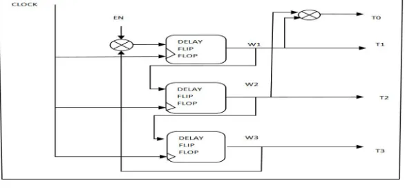
[image:3.612.162.455.544.680.2]The present work gives the BIST based approach for the implementation of a multiplier using a configurable hardware. A 4-bit low power multiplier design is used as a test logic design in the present work. The gate level architecture is used for the implementation of multiplier design. Representation for realizing the low-power hardware, to generate a half-adder and a full-adder design a gate level combination is used. To generate the multiplier using the adder terms these adder design blocks are used. A test pattern generator with random output value is required for the implementation of BIST. A low-power modified design of linear-feedback-shift-register (LFSR) is used in the implementation of this design for realization of TPG. For the generation of a 4-bit random number a 3 bit register is used. It is a comparative low power design realization as compared to other existing test power generator designs. Most of the TPG have a register-to-bit ratio of ‘1’. But in this proposed design, the TPG has a register-to-bit ration of 3:4. The test pattern generator logic block diagram is shown in Fig 2. Three flip-flops with a linear feed-back is used. The output of the last flip-flop is XOR-ed with the control input Enable in order to initiate the random number generation. The outputs of the first two flip-flops are XOR-ed to generate the fourth output bit of the TPG. Thus if Enable input is low then the output of the TPG will drive to logic “0000” output combination. An active high signal on the Enable input will activate the hardware to generate random 4-bit signal. The presented TPG can be used in multiple combinations, mixed or serial or parallel, for generating a random sequence of number with a higher length for other BIST based application realization. This circuit uses 3 registers to generate a 4-bit random value, so relatively very low power consumption is caused by this circuit.
Fig. 2 Logic diagram of test pattern generator
IV. GENERAL ATPG TESTING TECHNIQUE
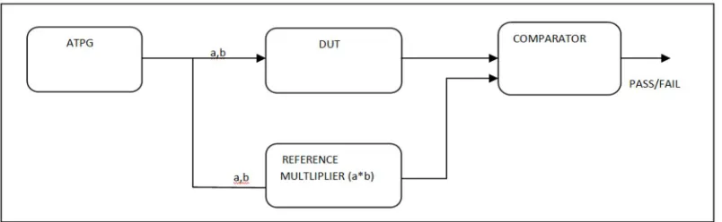
Another simple approach to test any circuit is general ATPG technique shown in figure 3 in which direct test patterns are applied through ATGP to the DUT and to reduce the complexity we use a reference multiplier is a multiplier which surely works and gives a correct output so this multiplier is taken as a reference in order to compare with the multipliers present in the DUT ( Vedic and Wallace Tree ) then comparator is used to compare the both of these outputs in order to determine the corrections of the multipliers, then comparator gives the results pass or fail. We are testing the multipliers by inserting faults in to them and whenever our assumed golden signatures value matches with ORA output then the results shows pass irrespective of fault values (0 or 1).
[image:4.612.110.512.239.363.2]Signature analysis is a method of compaction of system responses during testing where by the entire good response of the machine is compacted in to a good machine signature the actual circuit signature is generated during the process of testing in the CUT and then compared with the good machine signature, in order to determine whether the CUT is faultless or faulty. Signature is defined as a circuit’s statistical property, it is usually a number computed for circuit during testing from its responses with the property that faults in the circuits usually cause the signature to divert from that of good machines.
Fig. 3 Block Diagram for General ATPG Testing Technique
V. SIMULATIONS AND RESULTS
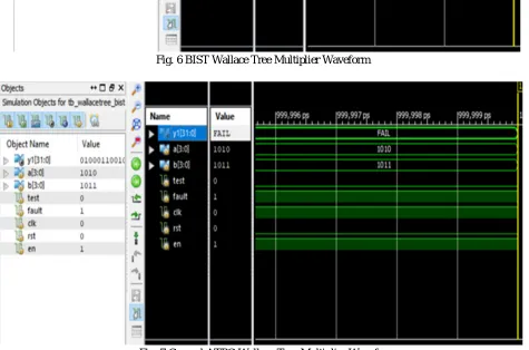
The BIST based Vedic and Wallace tree multipliers and general ATGP based Vedic and Wallace tree multipliers proposed in this work is implemented using Verilog on Xilinx ISE tool of version 14.7. The simulation wave form results of BIST based and ATGP based multipliers is shown in the below waveforms.
Fig. 4 BIST Vedic Multiplier Waveform
Fig. 6 BIST Wallace Tree Multiplier Waveform
[image:5.612.66.541.235.549.2]
Fig. 7 General ATPG Wallace Tree Multiplier Waveform
VI. CONCLUSION AND FUTURE WORK
In the present work the logic design that is used in the built in self test applications is a 4 bit multiplier and the test pattern Generator is also designed for generating a random 4 bit number. The test pattern generator is a modified design that has a Low register to bit ratio, which means, the number of output bits in the generated sequence is more than the number of
Registers in the Generated circuit. Thus, with respect to previously proposed design of TPG it involves less number of Registers and hence a low power design realization is obtained using this TPG. In this work we designed Vedic and Wallace
REFERENCES
[1] L. Supriya, J. Lingaiah and G. Kalyan, “FPGA Implementation of BIST (Built-in-Self-Test) Enabled UART for Real Time Interface Applications”, International Journal of Science, Engineering and Technology Research, Volume-4 Issue-7, pp.2645-2647, July 2015.
[2] Kavitha, G. Seetharaman, T. N. Prabhakar and Shrinithi, “Design of Low Power TPG using LP-LFSR”, International Conference on Intelligent Systems Modelling and Simulation, IEEE Computer Society, pp.334-338, 2012.
[3] Md. Fokhrul Islam, M. A. Mohd. Ali and Burhanuddin Yeop Majlis, “FPGA Implementation of an LFSR based Pseudorandom Pattern Generator for MEMS Testing”, International Journal of Computer Applications, Volume-75 No-11, pp.30-34, August 2013.
[4] Syed. Mujeeb Raheman and M. Basha, “Low Power Linear Feedback Shift Register based Low Power Test Pattern Generator”, International Journal and Magazine of Engineering, Technology, Management and Research, Volume-2 Issue-6, pp.579-584, June 2015.
[5] Mohammad Moinuddin and Sadgunn Kumari V, “FPGA implementation of 16-bit BBS and LFSR PN Sequence Generator”, International Journal of Scientific Engineering and Technology Research, Volume-4 Issue-31, pp.6082-6084, August 2015.
[6] Babitha P. K., Thushara T. and Dechakka M.P., “FPGA based N-bit LFSR to generate random sequence number”, International Journal of Engineering Research and General Science, Volume-3 Issue-3, pp.6-10, May-June 2015.
[7] Swapna S. and Sunilkumar S. Manvi, “Review of LP-TPG using LPLFSR for Switching Activities”, International Journal of Advanced Research in Computer Science and Software Engineering, Volume-5 Issue-2, pp.157-160, February 2015.
[8] Mirella Amelia Mioc, “A simulation study of TPG using Shift Register based on 16th Degree Primitive Polynomials”, New Developments in Pure and Applied Mathematics, pp.363-369, ISBN: 978-1-61804-287-3.
[9] V. Divya Bharathi and Arivasanth M., “Generation of Pseudo-Random number by using Well and Re-seeding method”, International Journal of Advanced Research in Electronics and Communication Engineering, Volume-4 Issue-3, pp.604-609, March 2015.
[10] Kaustubh M. Gaikwad and Mahesh S. Chavan, “Vedic Mathematics for Digital Signal Processing Operations: A Review”, International Journal of Computer Applications, Volume-113 N0-18, pp.10-14, March 2015.
[11] Neha Shaktawat and Ghanshyam Jangid, “FPGA Implementation of High Speed 16-Bits Vedic Multiplier using LFSR”, International Journal of Computer Science and Mobile Computing, Volume-4 Issue-8, pp.102- 108, August 2015.
[12] L. Supriya, J. Lingaiah and G. Kalyan, “FPGA Implementation of BIST (Built-in-Self-Test) Enabled UART for Real Time Interface Applications”, International Journal of Science, Engineering and Technology Research, Volume-4 Issue-7, pp.2645-2647, July 2015.