IJEDR1401023 International Journal of Engineering Development and Research ( www.ijedr.org)
135
New Control Approach for D- STATCOM
1
Shukla Darshan H.,
2Panchal Nilam B.
1Student , 2Asst.Professor.
1Electrical Dept, Kalol Institute Of Technology & Research Center, Kalol, India 2Electrical Dept, Kalol Institute Of Technology & Research Center, Kalol, India
1[email protected], 2[email protected]
Abstract— In distribution side the D-STATCOM gives good power quality response. The D-STATCOM operate VSI and energy storing device, the conventional topology can compensated reactive power from the line but the rating of storage device is increased. So in this topology if we used some arrangement/connection of small dc 2link capacitor then we can reduces the size of VSI and also dc-link voltage without compromising it’s compensation. In this paper the proposed method use to reduces the rating of VSI and dc-link voltage by some arrangement of small dc-link capacitor. This topology verify by simulation using MATLAB environment
.
Index Terms— Introduction, Design, Simulation, Conclusion
I.INTRODUCTION
In modern life the quality of electrical power is first preferences, every consumer wants electricity with quality. Now a days industries are spared within a small year, and the process of manufacturing also increases. Although in industries modern devices are used which can consume minimum time of production and increase the profit margin.
But that devices consist of static switching devices which have high ratio to produces unwanted condition in power quality, which can we say power quality problem like Sag, Swell etc. In distribution side FACT’s devices are used is called custom power device, which can give the quality of power at distribution side and satisfied the customers power quality need. In distribution side D-STATCOM(Distribution STATCOM) can give good response. Its working depends upon the VSC and storing devices connecting with it. But the rating of VSI become a bulky for it storing device to compensated the reactive power of the line, because the voltage of dc-link capacitor is 6 times of it’s system voltage[1].
In this paper we compensate the reactive power of system by proposed method of D-STATCOM, In this proposed method some arrangement /connection of small capacitor which can reduces the dc-link voltage rating without compromising its compensation of reactive power of line. By using this we reduce the rating of VSI and dc- link capacitor. The proposed method is verify by using MATLAB software.
II.D-STATCOMOPERATION
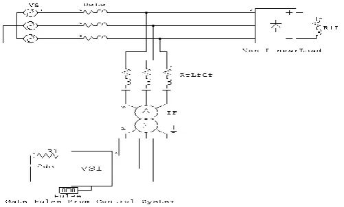
D-STATCOM (Distribution STATCOM) is used to improve the power quality at distribution side. This devices can able to absorb as well as generate the reactive power against variation of load. This device consist of VSI, Storing devices(dc-storing capacitor),coupling transformer etc. This are main parts of D-STATCOM connected in shunt mode to main line shown in fig (1) . Here Ia,Ib,Ic are source current and Ia’,Ib’Ic’ are load current and Ifa Ifb Ifc are compensating current of D-STATCOM.
Fig 1. Configuration of D-STATCOM
The operation of D-STATCOM depends the capacity of dc storing device. It work against the voltage variation at PCC. If the voltage at source side Vs grater then Load voltage Vr then it absorb the reactive power and if Vs is less then load voltage Vr then it generate reactive power.
IJEDR1401023 International Journal of Engineering Development and Research ( www.ijedr.org)
136
The reactive power generation by using VSI which triggering by control system of its gate pulse. In control system the PWM technique is used to give a gate pulse to VSI, This technique is more efficient then another control method. In VSI mostly IGBT static semiconductor devices which have low switching losses. Generally D-STATCOM devices is used for stiff source, non-stiff source means a sub-station which provide the electricity at remote area have some distance to load.III.CALCULATION OF D-STATCOM COMPONENT
The components of D-STATCOM like:
VSI(Voltage Source Inverter) Dc-Link Capacitor
Filter
Coupling Transformer
The calculation is as follow :
A.DCCAPACITOR VOLTAGE
Here first we calculate dc voltage Vdc of VSI [2].The DC Capacitor voltage should be grater then phase voltage of system The dc voltage is calculated by following equation.
Vdc= 22VLL Eqn.1.
3m
Where VLL is line to line voltage of a D-STATCOM, m is a modulation index , Vdc is a dc link voltage
.
B.DC BUS CAPACITOR
The value of DC bus capacitor value depends upon instantaneous energy available at D-STATCOM during transient. [2]. The value of this capacitor is calculated.
½ Cdc [(Vdc2 )-(Vdc1 )2 ]=3V(I)t Eqn. 2.
Where Cdc is value of capacitor Vdc and Vdc1 are references voltage and minimum voltage of dc bus, V is a phase voltage, I phase current, t is time by which dc bus voltage is recovered and overloading factor,
C.INDUCTOR
The value of inductor can be calculated the following equation, the value of [2] inductor depends upon current ripple ,switching frequency and dc bus voltage
Lf =3mVdc Eqn. 3.
12
f
si
cr(p-p)D.RIPPLE FILTER
Here the ripple filter the series capacitor is connected in series with inductor the [2] value is taken in this paper is depends upon the filter out high frequency noise. If we take line has low impedance 8.1ohm then take Cf = 5uF if high frequency noise is 5kHz.where Cf is series capacitor.
The whole diagram of D-STATCOM with all component are shown in fig 2.
IJEDR1401023 International Journal of Engineering Development and Research ( www.ijedr.org)
137
IV.CONTROL STRATEGYThe control strategy used to control the gate pulse system of VSI can be control using following control strategy. [3] Phase shift control
Decoupled Current Control(p-q theory) Regulation of ac bus and dc link voltage Synchronous Reference Frame Method(SRF) ADALINE based control method
In this paper use a SRF method. This method can able to control reactive power and active power separately by using Clark’s and Park’s transformation.
𝐼0
𝐼𝛼
𝐼𝛽
=
2/3
1 2
1 2
1 2
1
−1/2
−1/2
0
3/2 − 3/2
𝐼𝑎
𝐼𝑏
𝐼𝑐
Eqn. 4
Clark’s transformation
𝐼𝑑
𝐼𝑞
=sin 𝜃
cos 𝜃
cos 𝜃
− sin 𝜃
𝐼𝛼
𝐼𝛽
Eqn.5 Park’s TransformationIn this control strategy first convert the current of PCC Ia,Ib,Ic into Id,Iq, by using dq0 theory, then after compare this with reference Id*,Iq* and then again convert it into Id,Iq,I0 into Ia,Ib,Ic by using invers Park’s transformation and then give that signal to PWM which generate the pulses for VSI,the whole system configuration is given in fig(3).The references value should get by using PI controller. The reference value of Id and Iq are indicated by Id* and Iq*. The Id* can get from dc-link voltage by comparing reference value, and Iq* get by RMS value of current and comparing it with reference value
,
Fig 3. Control Strategy
V.PROPOSED CONTROL SYSTEM
In this paper the proposed method is implemented within VSI’s link capacitor of D-STATCOM, The design of VSI’s dc-link capacitor is most important part if the value of dc-dc-link value is not sufficient then working of VSI is not faithfully,
In conventional topology there is one capacitor is used which rating is somewhat higher another topology which used two capacitor[4] ,which can reduce the size of dc-link voltage of capacitor, In this topology if we used the arrangement /connection of small capacitor then can reduce the size of VSI and dc-link voltage without compromising it’s compensation. The arrangement shown in fig 4 .
IJEDR1401023 International Journal of Engineering Development and Research ( www.ijedr.org)
138
.The whole proposed Diagram is shown in fig 5.
Fig 5.Proposed Method System
VI.HOW IT REDUCE THE SIZE OF CAPACITOR
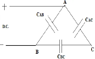
If we compare it with stored energy equation:-
½ CV2 = ½ Ceq V2 Eqn 6. If Suppose Ceq=C
Where C=C AB+CBC*CCA Eqn.7 CBC+CCA
So put that value in equation We get
C=2/3 C Eqn 8 And that will apply to find the Vdc
So,
½ C[Vdc2-Vdc12 ]= P(inverter) Eqn.9 ½ C[ Vdc2-Vdc12] = 3*V*I**t[2] Eqn.10
Where V=System line Voltage I= Line Current =Overloading Factor t= Time Period of Switching
From put Eqn (8) into eqn (10) we get
1/3 C [Vdc2-Vdc1 2
]=3*V*I**t
Eqn.11 VII.MATHEMATICALMODELOFPROPOSED METHOD:-
IJEDR1401023 International Journal of Engineering Development and Research ( www.ijedr.org)
139
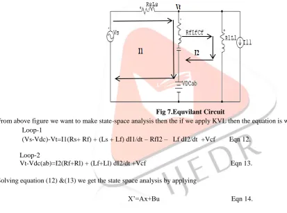
Fig 6.Mathamtical ModelFrom above single line diagram can be reduces by using eqn.(8) we can draw the equivalent as shown in fig 7.
Fig 7.Equvilant Circuit
From above figure we want to make state-space analysis then the if we apply KVL then the equation is written Loop-1
(Vs-Vdc)-Vt=I1(Rs+ Rf) + (Ls + Lf) dI1/dt – RfI2 – Lf dI2/dt +Vcf Eqn 12. Loop-2
Vt-Vdc(ab)=I2(Rf+Rl) + (Lf+Ll) dI2/dt +Vcf Eqn 13.
Solving equation (12) &(13) we get the state space analysis by applying
X’=Ax+Bu Eqn 14.
Here X1=I1,X1’=dI1/dt, X2=I2,X2’=dI2/dt, X3=Vcf=1/𝐶 𝑖2𝑑𝑡
If taken a source side then the state variable become
𝑋1′ 𝑋2′ 𝑋3′
=
(𝑅𝑠 + 𝑅𝑓) (𝐿𝑠 + 𝐿𝑓) 0
0 −𝑅𝑓 0
0 1 1
𝑥1 𝑥2 𝑋2 + (𝑉𝑠 − 𝑉𝑑𝑐) − 𝑉𝑡) 0 0
u Eqn 15.
If take a load side then the State space is become
𝑋1′ 𝑋2′ 𝑋3′
=
0 (𝑅𝑓 + 𝑅𝑙) 0
0 0 (𝐿𝑓 + 𝐿𝑙)
0 0 1
𝑥1 𝑥2 𝑋2 + (𝑉𝑡 − 𝑉𝑑𝑐(𝑎𝑏)) 0 0
IJEDR1401023 International Journal of Engineering Development and Research ( www.ijedr.org)
140
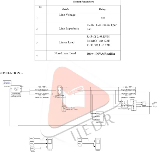
VIII.SIMULATIONWORKHere to verify the topology the data of a system is give below here the load non-linear just like rectifier.
System Parameters
Sr.
Details Ratings
1.
Line Voltage
440
2. Line Impedance
R=1 L=0.034 mH per line
3. Linear Load
R=34 L=0.154H R= 81 L=0.125H R=31.5 L=0.22H
4. Non-Linear Load 10kw 100VArRectifier
IX.SIMULATION
:-Fig 8. Simulation Diagram
X.SIMULATION RESULT
IJEDR1401023 International Journal of Engineering Development and Research ( www.ijedr.org)
141
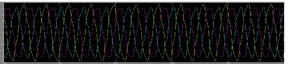
Fig 10.Without Compensation Current .Now we observe the result by compensating using conventional method in fig 11a,11b.
Fig.11a.Compensated voltage of system by using conventional method
Fig 11b.Compensated Current of system by using conventional method
Now the result of proposed method in fig 12a,12b
IJEDR1401023 International Journal of Engineering Development and Research ( www.ijedr.org)
142
Fig 12b. .Compensated Current of system by using proposed methodThe THD by all above method is given table :-
THD(%)
Without Compensation Conventional
Method Proposed Methods
Isa
9.57
8.00
5.00
Isb
9.74
8.00
6.00
Isc
11.21
6.00
4.00
Vsa
18.00
10.00
8.00
Vsb
18.30
12.00
8.00
Vsc
19.00
14.00
10.00
This also analyses by observing Chart of THD of system current
Fig 13. Chart of system current %THD Fig 14. Chart of system Voltage %THD
XI.CONCLUSION:-
IJEDR1401023 International Journal of Engineering Development and Research ( www.ijedr.org)
143
XII.REFERENCES:-[1] IEEE TRANSACTIONS ON POWER ELECTRONICS, VOL. 27, NO. 3, MARCH 2012 A DSTATCOM Topology With Reduced DC-Link Voltage Rating for Load Compensation With Nonstiff Source, Srinivas Bhaskar Karanki, Nagesh Geddada, Student Member, IEEE, Mahesh K. Mishra, Senior Member, IEEE, and B. Kalyan Kumar, Member, IEEE
[2] International Journal of Advances in Engineering & Technology, Jan 2012. A ZIGZAG-DELTA PHASE-SHIFTING TRANSFORMER AND THREE-LEG VSC BASED DSTATCOM FOR POWER QUALITY IMPROVEMENT R.Revathi1 and J.Ramprabu2 1PG Student, Department of Electrical and Electronics Engineering, Kumaraguru College of Technology, Coimbatore-641 049, India 2Assistant Professor, Department of Electrical and Electronics Engineering, Kumaraguru College of Technology, Coimbatore-641 049, India
[3] Power Quality Improvement by using DSTATCOM P. Bapaiah
[4] IEEE TRANSACTIONS ON POWER ELECTRONICS, A Modified DSTATCOM Topology with Reduced VSI Rating, DC Link Voltage, and Filter Size Chandan Kumar∗, Mahesh K. Mishra∗∗, Senior Member, IEEE Department of Electrical Engineering, Indian Institute of Technology Madras, Chennai, India ∗Corresponding Author: Tel.:+91 44 2575459; Fax:+91 44 22574402; E-mail: [email protected]∗∗E-mail: [email protected]
[5] INTERNATIONAL CONFERENCE ON ―CONTROL, AUTOMATION, COMMUNICATION AND ENERGY CONSERVATION-2009, 4th-6tH June 2009, Analysis of DSTATCOM with BESS for Mitigation of Flicker Vasudeo Virulkar Student Member, IEEE and Mohan Aware.