Implementation Fault Tolerant Full Adder/Subtractor Using
Reversible Logic Gates
D.Swathi & B.Shiva Kumar
1.
Pg Scholar, Department of ECE, Vaagdevi College of Engineering, Bollikunta Warangal, Telangana2.Assistant Professor, Department of ECE, Vaagdevi College of Engineering, Bollikunta Warangal, Telangana
ABSTRACT Reversible logic is most popular
concept in energy efficient computations and this will be demand for upcoming future computing technologies. Reversible logic is emerging as an important research area and it will be having wide applications in many fields such as optical information processing, quantum computing and Low power CMOS design. Under ideal conditions, the reversible logic gates will produce zero power dissipation. So this concept will helpful for Low power VLSI design. This paper will proposes the design of Full adder/subtractor circuit using fault tolerant reversible gates. The design can work singly as an adder/subtractor. The proposed design offers less hardware complexity and is efficient in terms of gate count, delay, constant inputs and garbage outputs compared to previous Fault tolerant Full Adder/Subtractor design. A parallel adder/subtractor design using fault tolerant reversible gates also proposed in this paper. The proposed circuits will be simulated using ModelSim simulator and implemented in Xilinx FPGA platform.
Keywords – Adder/Subtractor, Parity preserving reversible gates, Parallel Adder/Subtractor, Reversible logic gates.
I. INTRODUCTION Today’s new technology
temperature. At a temperature T for one bit loss it will generates 2.86 10-21 J of energy that will be small but we cannot neglect this value. The heat dissipated in the circuit will gradually decrease the performance and also life span of the circuit or device. In order to overcome these types of problems we require low power consumption and less dissipation components in the circuit. C H Bennet [2] shown that if we use reversible logic gates instead of irreversible components in the circuit, we can achieve zero energy dissipation in the circuit. He proposed two conditions of reversibility.
1 st condition: For any device to be reversible if
its input and output will be uniquely retrievable from each other called logical reversibility.
2 nd condition: A device can run actually
backwards then it is called physically reversible.
The reversible circuits are those in which reversible logic gates are basic building blocks and there is no energy loss. The reversible logic gates will be having n-input and n-output i.e. equal number of input and equal number of output, and also with oneto-one mapping i.e. inputs can be uniquely recovered from the outputs.
LITERATURE REVIEW:
Reliable computing and quantum computing is one ofthe emerging areas in today’s world. Berger
to detect unidirectional errors. In case of parity preserving technique, if multiple errors occurs on the same line then it cannot detect them, as one error may cancel other. Hence this technique cannot detect multiple errors.
In"Irreversibility and Heat Generation in the
Computing Process” It is argued that computing
machines inevitably involve devices which perform logical functions that do not have a single-valued inverse. This logical irreversibility is associated with physical irreversibility and requires a minimal heat generation, per machine cycle, typically of the order of kT for each irreversible function. This dissipation serves the purpose of standardizing signals and making them independent of their exact logical history. Two simple, but representative, models of bistable devices are subjected to a more detailed analysis of switching kinetics to yield the relationship between speed and energy dissipation, and to estimate the effects of errors induced by thermal fluctuations
IN “DESIGN OF LOW POWER
COMPARATOR USING DG GATE” In recent
studies, reversible logic has emerged as a great scene of research, having applications in low power CMOS circuits, optical computing, quantum computing and nanotechnology. The classical logic gates such as AND, OR, EXOR and EXNOR are not reversible. In the existing
literature, reversible sequential circuits designs are offered that are improved for the number of the garbage outputs and reversible gates. Minimizing the number of garbage is very noticeable. In the present paper, we show a design of the reversible comparator based on the quantum gates implementation of the reversible DG gate. The reversible DG gate is designed by using 3 × 3 quantum gates such as NOT, CNOT, Controlled-V and Controlled-V+ gates. Also, we have used the TR gate and various types of quantum gates in the implementation results. Low power three-bit comparator is designed using DG Gate, New Gate and Fredkin Gate. In order to evaluate the benefit of using the DG gate proposed in this paper, one-bit comparator is constructed. The design is useful for the future computing techniques like quantum computers. The proposed designs are implemented using VHDL and functionally investigated using Quartus II simulator.
In “Optimized Nanometric Fault Tolerant
Reversible BCD Adder”In recent years,
well as a fault tolerant reversible Carry Skip BCD adder. We have proposed new reversible fault tolerant gates and heuristic algorithms to design compact BCD Adders. The proposed reversible fault tolerant BCD adder achieves the improvement as reducing cost of 23.07% on the number of gates, 52.67% on quantum cost, 31.03% on garbage outputs, 29.16% on the number of constant inputs and 23.07% on unit delay over the existing best one. Similarly, the proposed reversible fault tolerant carry skip BCD adder achieves the improvement as reducing cost of 34.72% on the number of gates, 43.24% on quantum cost, 37.5% on garbage outputs, 37.14% on the number of constant inputs and 34.72% on unit delay over the existing best one.
In "Fault-Tolerant Reversible Circuits”
Reversible hardware computation, that is, performing logic signal transformations in a way that allows the original input signals to be recovered from the produced outputs, is helpful in diverse areas such as quantum computing, low-power design, nanotechnology, optical information processing, and bioinformatics. We propose a paradigm for performing such reversible computations in a manner that renders a wide class of circuit faults readily detectable at the circuit's outputs. More specifically, we introduce a class of reversible logic gates (consisting of the well-known Fredkin gate and a newly defined Feynman
double-gate) for which the parity of the outputs matches that of the inputs. Such parity-preserving reversible gates, when used with an arbitrary synthesis strategy for reversible logic circuits, allow any fault that affects no more than a single logic signal to be detectable at the circuit's primary outputs. We show the applicability of our design strategy by demonstrating how the well-known, and very useful, Toffoli gate can be synthesized from parity- preserving gates and apply the results to the design of a binary full-adder circuit, which is a versatile and widely used element in digital arithmetic processing
Reversible Logic Gates
The main object in reversible logic theory is the reversible function, which is defined as follows.
Definition1. The multiple output Boolean function
F(x1; x2; :::; xn) of n Boolean variables is called reversible if:
1. The number of outputs is equal to the number of inputs;
2. Any output pattern has a unique preimage. In other words, reversible functions are those that perform permutations of the set of input vectors.
Definition2. Garbage is the number of outputs
added to make an n-input k-output function ((n; k) function) reversible.
function to make it reversible. The following simple formula shows the relation between the number of garbage outputs and constant inputs Input + constant input = output + garbage.
The Quantum Cost of 1*1 Reversible gates is zero, and Quantum Cost of 2*2 Reversible gates is one. Any Reversible gate is realized by using 1*1 NOT gates and 2*2 Reversible gates, such as V, V+ and FG gate which is also known as CNOT gate. The V and V+ Quantum gates have the property given in the Equations 1, 2 and 3.
V * V = NOT ……… (1) V * V+ = V+ * V = I ……….. (2) V+ * V+ = NOT ………. (3)
The Quantum Cost of a Reversible gate is calculated by counting the number of V, V+ and CNOT gates [2],[3].
2.1 NOT Gate
The simplest Reversible gate is NOT gate and is a 1*1 gate. The Reversible 1*1 gate is NOT Gate with zero Quantum Cost is as shown in the Figure 1.
2.2 Feynman / CNOT Gate
Controlled NOT (CNOT) gate is an example for a 2*2 gate. The Reversible 2*2 gate with Quantum Cost of one having mapping input (A, B) to output (P = A, Q = A B) is as shown in the Figure 2.
There are many 3*3 Reversible gates such as F, TG, PG and TR gate.
REVERSIBLE GATES
There are many reversible gates such as Feynman, Toffoli, TSG, Fredkin, Peres, etc [3]. As the universal gates in boolean logic are Nand and Nor, for reversible logic, the universal gates are Feynman and Toffoli gates.
Feynman Gate: Feynman gate is a universal gate
Fredkin Gate: It is a basic reversible 3- bit gate used for swapping last two bits depending on the control bit. The control bit here is A, depending on the value of A, bits B and C are selected at outputs Q and R. When A=0, (Q=B, R=C) whereas when A=1, (Q=C, R=B). Its block diagram is as shown in fig. 2:
Peres Gate: It is a basic reversible gate which has
3- inputs and 3-outputs having inputs (A, B, C) and the mapped outputs (P=A, Q=A^B, R=(A.B)^C). The block diagram is as shown in fig. 3:
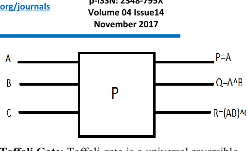
Toffoli Gate: Toffoli gate is a universal reversible
gate which has three inputs (A, B, C) mapped to three outputs (P=A, Q=B, R= (A.B)^C). The block diagram of Toffoli gate is shown in fig. 4:
TSG Gate: TSG gate is a reversible gate which
has four inputs (A, B, C, D) mapped to four
outputs (P=A, Q=A^B, R=A^B^D,
S=(A^B)^D^AB^C). The block diagram of TSG Gate is shown in fig. 5:
Modified IG Gate (MIG): Fig. 4 shows 4*4 Modified IG [7] gate. It has A, B, C and D input vector and output vector as P = A, Q = A⊕ B, R = AB ⊕C and S = AB’⊕D.
Modified IG Gate (MIG) Parity Preserving Reversible Gate (P2RG): Fig.5 shows 5*5 parity preserving reversible gate [10], P2RG. It has A, B, C, D and E input vector and output vector as P=A, Q= (A’C’⊕B’) ⊕D, R= (A’C’⊕B’) D⊕AB⊕C, S=AB’⊕C⊕ (A’C’⊕B’)’D and T= (D⊕E)
⊕AC.
Parity Preserving Reversible Gate (P2RG)
Full Adder is design by use MIG and COG based Reversible Logic gate. The proposed design model contain control signal which is using for control the adder and subtractor operation. Figure 6 is showing the diagram for MIG (Modified Islam Gate). In this four inputs and 4 Output are using. Figure 7 is showing the COG Gate which has 3 Input and 3 Output. Figure 8 is showing the proposed circuit for design Fault Tolerant Full Adder / Subtraction. In this two MIG gates are using and one COG gate is using. There are A, B, C, Cntrl are in input and C/B and S/C are the output. The control signal is using for control the operation of Adder / Subtraction. For the Logic, 0 Adder will work, and for Logic 1 Subtractor will work.
APPLICATIONS The reversible logic will have many applications. Some important areas of reversible logic include the following [13, 14]
Nanocomputing
Bio Molecular Computations
Laptop/Handheld/Wearable Computers
Spacecraft
Low power CMOS.
Design of low power arithmetic and data path for digital signal processing (DSP).
CONCLUSION AND FUTURE WORK This
paper presents efficient approach for the design of fault tolerant full adder/subtractor and parallel adder/subtractor. The proposed design can work as single unit that can acts as adder as well as
subtractor depending upon our requirement. The proposed design offers less hardware complexity, less gate count, less garbage bits and constant inputs. The reversible computation can be done efficiently with less number of garbage bits and constant inputs. The proposed Fault tolerant Adder/Subtractor design can be used to realize some arithmetic components such as carry save adder, carry skip adder and multiplier/divisors etc,. In future we are planning to design more optimized Fault tolerant Adder/Subtractor design and other fault tolerant circuits i.e. less garbage bits and constant input.
REFERENCES
[2] C.H. Bennett, “Logical Reversibility of Computation”, IBM J. Research and Development, pp. 525-532, November 1973.
[3] Hafiz Md. Hasan babu, Md. Rafiqu Islam, Ahsan Raja Chowdhary and Syed Mostahead Ali chowdhary “ Reversible logic synthesis for minimization of full adder ckt”, IEEE conference
on Digital system design
2003,Enromicro‟03,Belek,Antalya,Tarkey, 2003,PP 50-54
[4] Hafiz Md. Hasan babu, Md. Rafiqu Islam, Ahsan Raja Chowdhary and Syed Mostahead Ali chowdhary “Synthesis of full adder ckt using Reversible logic”.17th international conference on VLSI Design 2004, Mumbai, India 2004, PP 757-760.
[5] Feynman R., 1985. Quantum mechanical computers, Optics News, 11: 11-20.
[6] Peres, A. 1985. Reversible logic and quantum computers. Physical Review A, 32: 3266-3276.
[7] E. Fredkin, T. Toffoli, “Conservative Logic”, International Journal of Theory of Physics, 21, 1982, pp 219-253.
[8] Toffoli T., 1980. Reversible computing, Tech Memo MIT/LCS/TM-151, MIT Lab for Computer Science.
[9] B. Parhami , “Fault tolerant reversible circuits”, in Proceedings of 40th Asimolar Conf. Signals, Systems, and Computers, Pacific Grove, CA, pp. 1726-1729, October 2006.
[10] E. Fredkin and T. Toffoli, “Conservative logic”, Intl. Journal of Theoretical Physics, pp. 219-253, 1982.
[11] Islam S. and M. Mahbubur Rahman, 2009b. Efficient Approaches for Designing Fault Tolerant Reversible Carry Look-Ahead and Carry- Skip Adders, MASAUM Journal of Basic and Applied Sciences, 1(3): 354-360.
[12] Parminder Kaur & Balwinder singh Dhaliwal “Design of Fault Tolerant Full Adder/Subtractor Using Reversible Gates” 2012 International Conference on Computer Communication and Informatics (ICCCI -2012), Jan. 10 – 12, 2012, Coimbatore, INDIA 978-1-4577-1583-9/ 12/ $26.00 © 2012 IEEE
[13] Michael P. Frank, Reversibility for efficient computing, Ph. D. Thesis, May 1999. http://www.cise.ufl.edu/-mpf/rc/thesis