Power-Efficient Carry Select Adder
A S Keerthi Nayani & Aruna Kokkula
Assistant Professor Matrusri Engineering College Hyderabad
Abstract-To reduces the power consumption of data path we need to reduce Area of the adder. Carry Select Adder is one of the fast adder used in may data path applications. The proposed design is implemented without using multiplexer and RCA structure with Cin=1. This paper proposes on the logic operations in conventional carry select adder (CSLA) and binary to excess-1 converter (BEC)-based CSLA to study the data dependency and to identify redundant logic operations. To overcome this problem, a SQRT-CSLA based on CBL was proposed. However, the CBL-based SQRT CSLA design requires more logic resource and delay than the BEC-based SQRT-CSLA. We observe that logic optimization largely depends on availability of redundant operations in the formulation, whereas adder delay mainly depends on data dependence.
I. INTRODUCTION
High-speed data path logic systems are one of the most substantial areas of research in VLSI system design. The speed of addition is limited by the time required to propagate a carry through the adder in digital adders. The sum for each bit position in an elementary adder is generated sequentially only after the previous bit position has been summed and a carry propagated into the next position. The CSLA is used in many computational systems to alleviate the problem of carry propagation delay by independently generating multiple carries and then select a carry to generate the sum the CSLA is not area efficient because it uses multiple pairs of Ripple Carry Adders (RCA) to generate partial sum and carry. Design of high speed data path logic systems are one of the most substantial research area in VLSI system design. High-speed addition and multiplication has always been a fundamental requirement of high-performance processors and systems [1].
The major speed limitation in any adder is in the production of carries and many authors have considered the addition problem. The basic idea of the proposed work is using n-bit binary to excess-1 code converters (BEC) to improve the speed of addition. The detailed structure and function of BEC. This logic can be implemented with any type of adder to further improve the speed [2]. The proposed 16, 32 and 64-bit adders are compared in this paper with the conventional fast adders such as carry save adder (CSA) and carry look ahead adder (CLA). This paper has realized the improved performance of the CSA with BEC logic through custom design and layout.
The final stage CPA constitutes a dominant component of the delay in the parallel multiplier. Signals from the multiplier partial products summation tree do not arrive at the final CPA at the same time. This is due to the fact that the number of partial-product bits is larger in the middle of the multiplier tree. Due to
un-even arrival time of the input signals to the final CPA, the selection of the ASIC Implementation of Modified Faster Carry Save Adder 54 final adder is an important work in parallel multipliers [3]. Therefore decrease in carry propagation delay will result in major enhancement of the speed of the adder and multiplier. This paper is structured as follows. In Section 2, an overview of the 4-bit binary to excess-1 logic is provided. Section 3 deals with the proposed modified carry save adder (MCSA) architecture. Among the myriad of aggressive techniques, carry select adder (CSL) has been an eminent technique in the space-time tug-of-war of CPA design. It exhibits the advantage of logarithmic gate depth as in any structure of the distant-carry adder family. Conventionally, CSL is implemented with dual ripple-carry adder (RCA) with the carry-in of 0 and 1, respectively.
Depending on the configuration of block length, CSL is further classified as either linear or square root. The basic idea of CSL is anticipatory parallel computation. Although it can achieve high speed by not waiting for the carry-in from previous sub-block before computation can begin, they consume more power due to doubling the amount of circuitry needed to do the parallel addition of which half of the speculative computations will be redundant.
after the previous bit position has been summed and a carry propagated into the next position.
The CSLA is used in many computational systems to alleviate the problem of carry propagation delay by independently generating multiple carries and then select a carry to generate the sum in reference1. However, the CSLA is not area efficient because it uses multiple pairs of Ripple Carry Adders (RCA) to generate partial sum and carry by considering carry input Cin=0 and Cin =1, then the final sum and carry are selected by the multiplexers (MUX). The basic idea of this work is to use Binary to Excess- 1 converter (BEC) instead of RCA with Cin = 1 in the regular CSLA to achieve lower area and power consumption in ref 2–4. The main advantage of this BEC logic comes from the lesser number of logic gates than the n-bit Full Adder (FA) structure [6].
The details of the BEC logic are discussed. Carry-ripple adder (CRA) is the simplest approach. However, the carry-look ahead adder (CLA) and its fast version, the parallel-prefix CLA, is the selected scheme for time-critical applications with a considerable cost in terms of silicon area and power dissipation. The CSA provides a compromise between a RCA and a CLA adder. Due to rapidly growing system-on-chip industry, not only the faster units but also smaller area and less power has become a major concern for designing very large scale integration (VLSI) circuits [7]. Digital circuits make use of digital arithmetic’s. Among various arithmetic operations, multiplication is one of the fundamental operation used and is being performed by an adder.
Objective
1. The basic idea of this work is to use Binary to Excess- 1 converter (BEC) instead of RCA with Cin = 1 in the regular CSLA to achieve lower area and power consumption.
2. The main advantage of this BEC logic comes from the lesser number of logic gates than the n-bit Full Adder (FA) structure.
Existing System
1. High-speed addition and multiplication has always been a fundamental requirement of high-performance processors and systems. The major speed limitation in any adder is in the production of carries and many authors have considered the addition problem.
2. High-speed data path logic systems are one of the most substantial areas of research in VLSI system design. The speed of addition is limited by the time required to propagate a carry through the adder in digital adders
3. . More power consumption.
Disadvantages of Existing
Today, one of the major challenges for high-performance microelectronic systems is the power dissipation, both static and dynamic
The circuit designer must, therefore, find an optimum between power and speed, instead of targeting them independently, and this is represented by the power-delay product, which represents the average energy dissipated for one switching event
Addition is by far the most fundamental arithmetic operation. It has been ranked the most extensively used operation among a set of real-time digital signal processing benchmarks from application-specific DSP to general purpose processors
Carry-propagation adder (CPA) is frequently part of the critical delay path limiting the overall system performance due to the inevitable carry propagation chain.
Proposed System
A structure of 4-bit BEC and the truth table is shown. How the goal of fast addition is achieved using BEC together with a multiplexer (mux) is described, one input of the 8:4 mux gets as it input (B3, B2, B1, and B0) and another input of the mux is the BEC output. This produces the two possible partial product results in parallel and the muxes are used to select either BEC output or the direct inputs according to the control signal Cin.
Advantages of Proposed
In this study, we investigate design methods to minimize the power-delay product of 64-bit adders in partially depleted (PD) silicon-on-insulator (SOI) technology.
The improvement of the power-delay product will be performed at the different hierarchical levels of the design: circuit design style, cell decomposition, and global architecture. A new architecture to reduce area and power of CSA. Adders with very large words sizes are constructed hierarchically by combining smaller “block” adders
A square root scheme with a new add-one circuit using one inverter instead of two-inverter buffer has been proposed. The proposed CSL outperforms the recently reported CSLs in both power-delay product and area-delay product. The basic idea of the proposed work is using n-bit binary to excess-1 code converters (BEC) to improve the speed of addition.
This logic can be implemented with any type of adder to further improve the speed. The improved performance of the CSA with BEC logic through custom design and layout.:
In this research, based on the idea of sharing the two adders that are typically used in the CSA, a new architecture is proposed which is more compact and power efficient than the CSA.
II. LOW-POWER AND AREA-EFFICIENT CARRY SELECT ADDER
The carry select adder generally consists of two ripple carry adders and a multiplexer. Adding two n-bit numbers with a carry select adder is done with two adders (therefore two ripple carry adders) in order to perform the calculation twice, one time with the assumption of the carry being zero and the other assuming one. After the two results are calculated, the correct sum, as well as the correct carry, is then selected with the multiplexer once the correct carry is known. The carry select adder partitions the adder into several groups, each of which performs two additions in parallel. Therefore, two copies of ripple-carry adder act as carry evaluation block per select stage. One copy evaluates the array chain assuming the block carry-in is zero, while the other assumes it to be one.
The conventional n-bit CSA consists of one n/2-bit adder for the lower half of the bits and two n/2-bit adders for the upper half of the bits. Of the two latter adders, one performs the addition with the assumption that Cin=0, whereas the other does this with the assumption that Cin=1. Using a multiplexer and the value of carry out that is propagated from the adder for the n/2 least significant bits, the correct value of the most significant part of the addition can be selected. Although this technique has the drawback of increasing the area, it speeds up the addition operation. A 16-bit carry select adder with a uniform block size of 4 can be created with three of these blocks and a 4-bit ripple carry adder. Since carry-in is known at the beginning of computation, a carry select block is not needed for the first four bits.
The delay of this adder will be four full adder delays, plus three MUX delays. Two 4-bit ripple carry adders are multiplexed together, where the resulting carry and sum bits are selected by the carry-in. Since one ripple carry adder assumes a carry-in of 0, and the other assumes a carry-in of 1, selecting which adder had the correct assumption via the actual carry-in yields the desired result. The carry select adder comes in the category of conditional sum adder. Conditional sum adder works on some condition. Sum and carry are calculated by assuming input carry as 1 and 0 prior the input carry comes. When actual carry input arrives, the actual calculated values of sum and carry are selected using a multiplexer.
The conventional carry select adder consists of k/2 bit adder for the lower half of the bits i.e. least significant bits and for the upper half i.e. most significant bits (MSB’s) two k/ bit adders. In MSB adder’s one adder assumes carry input as one for performing addition and another assumes carry input as zero. The carry out calculated from the last stage i.e. least significant bit stage is used to select the actual calculated values of output carry and sum. The selection is done by using a multiplexer. This technique of dividing adder in to stages increases the area
utilization but addition operation fastens. For an n bit adder, it could be implemented with equal length of carry select adder, and this is called linear carry select adder.
However. The linear carry select adder does not always have the best performance. A carry select adder can be implemented in different length, and this is called nonlinear carry select adder. A carry-select adder is divided into sectors, each of which – except for the least significant – performs two additions in parallel, one assuming a carry-in of zero, the other a carry-in of one. Using the idea of CSA iteratively, the delay of the adder can significantly be reduced. It can be shown that if the delay of multiplexers is negligible, the delay of the iterative CSA will grow with the square root of the number of bits. A more accurate analysis is required to find the delay of CSA if the delay of multiplexers is not negligible. In the following, such an analysis is presented and will be confirmed with simulation results. The 16-bit adder blocks are implemented as carry-select adders, with 4-bit adder blocks having a carry-in either at “0” or at “1.” At the 16-bit level, the same CS-boxes be used as at the 64-bit level, sizing of the transistors being adapted to the particular load conditions.
The 4-bit adder blocks can finally be implemented as ripple adders, or also as carry-select adders, which was chosen here. The carry-select architecture is thus used at three different levels: in the 64-bit, the 16-bit, and the 4-bit adders. The main advantage of this logic is that each group computes the partial results in parallel and the mux’s are ready to give the final result “immediately” with the minimum delay of the mux. When the Cin of each group arrives, the final result will be determined “immediately”. Thus the maximum delay is reduced in the carry propagation path. This same logic has been used for 32 and 64-bit adder structures to achieve higher speeds. Table 2 exhi64-bits the post layout simulation results of adder structures in terms of delay, area and power. The area indicates the total cell area of the design and the total power is sum of leakage power, internal power, net power and dynamic power.
The block level representation of Floating Point Carry-Save multiplication is implemented. The n-Input pins supply normalized multiplicand (having implicit 1 to the left of binary point) and n-more supply multiplier bits. Instead of carrying out “AND” operation in each block itself, the ANDed bits are produced all at once in an ANDer block and then introduced at the proper position. These ANDed signals are then added in Carry-Save floating-point representation to get the final product. The ANDed signals are introduced at their proper position within the floating-point multiplier. This calculates unnormalized (i.e. without implicit 1 to the left of the binary decimal point) floating-point product.
The product is then passed through the normalizer block. This block normalizes the product if required depending upon the control signal in the standard IEEE format. The normalized product is then outputted through the mode selector, which depending upon the mode selected gives either n-bit precise output in 1 cycle or n-bit product extended over two clock cycles. In case the product needs to be normalized, the exponent out from the exponent block is accordingly adjusted. The device also raises flag bits indicating the state of the output.
III. CARRY SELECT ADDER DESIGN
A multiplier is one of the key hardware blocks in most digital and high performance systems such as FIR filters, digital signal processors and microprocessors etc. With advances in technology, many researchers have tried and are trying to design multipliers which offer either of the following- high speed, low power consumption, regularity of layout and hence less area or even combination of them in multiplier. However area and speed are two conflicting constraints. So improving speed results always in larger areas. So here we try to find out the best trade off solution among the both of them. Generally as we know multiplication goes in two basic steps.
Hence in this paper we have first tried to design different adders and compare their speed and complexity of circuit i.e. the area occupied. And then we have designed Wallace tree multiplier then followed by Booth’s Wallace multiplier and have compared the speed and Power consumption in them. While comparing the adders we found out that Ripple Carry Adder had a smaller area while having lesser speed, in contrast to which Carry Select Adders are high speed but posses a larger area. And a Carry Look Ahead Adder is in between the spectrum having a proper tradeoff between time and area complexities. After designing and comparing the adders we turned to multipliers. Initially we went for Parallel Multiplier and then Wallace Tree Multiplier. In the mean time we learned that delay amount was considerably reduced when Carry Save Adders were used in Wallace Tree applications. Then we turned to Booths Multiplier and designed Radix-4 modified booth multiplier and analyzed the performance of all the multipliers. After that we turned to different methods
of power optimization, of which we could only complete a few like we went for designing different recoding schemes and their corresponding partial product generator scheme.
After that we designed these recoders and PP generators and found out the time delays and area covered and power consumed by each scheme. We took into consideration that since all the PP generators take a huge amount of area we need to go for simplest of the designs for them and also side by side we need to ensure that we don’t have much switching actions in the circuit. As the scale of integration keeps growing, more and more sophisticated signal processing systems are being implemented on a VLSI chip. These signal processing applications not only demand great computation capacity but also consume considerable amount of energy. While performance and Area remain to be the two major design tolls, power consumption has become a critical concern in today’s VLSI system design.
The need for low-power VLSI system arises from two main forces. First, with the steady growth of operating frequency and processing capacity per chip, large currents have to be delivered and the heat due to large power consumption must be removed by proper cooling techniques. Second, battery life in portable electronic devices is limited. Low power design directly leads to prolonged operation time in these portable devices. Multiplication is a fundamental operation in most signal processing algorithms. Multipliers have large area, long latency and consume considerable power. Therefore low-power multiplier design has been an important part in low- power VLSI system design. There has been extensive work on low-power multipliers at technology, physical, circuit and logic levels.
A system’s performance is generally determined by the performance of the multiplier because the multiplier is generally the slowest element in the system. Furthermore, it is generally the most area consuming. Hence, optimizing the speed and area of the multiplier is a major design issue. However, area and speed are usually conflicting constraints so that improving speed results mostly in larger areas. As a result, a whole spectrum of multipliers with different area- speed constraints has been designed with fully parallel. Fully In between are digit serial multipliers where single digits consisting of several bits are operated on. These multipliers have moderate performance in both speed and area. However, existing digit serial multipliers have been plagued by complicated switching systems and/or irregularities in design.
IV. SIMULATION IMPLEMENTATION
carry by considering carry input Cin=0 and cin=1, then the final sum and carry are selected by the multiplexers (mux). The sum for each bit position in an elementary adder is generated sequentially only after the previous bit position has been summed and a carry propagated into the next position
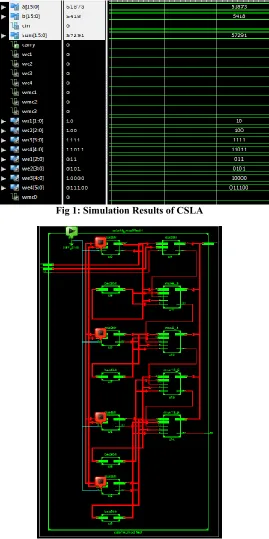
Fig 1: Simulation Results of CSLA
Fig 2: RTL Schematic for CSLA
In VLSI system design the design of area and power efficient high speed logic systems are most essential. In digital adders, the speed of addition is limited by the time required to propagate a carry through the adder. The sum for each bit position in an elementary adder is generated sequentially only after the previous bit position has been summed and a carry propagated into the next position.
CSLA is used in many computational systems to alleviate the problem of carry propagation delay by independently generating multiple carries and then select a carry to generate the sum. However, the CSLA is not area efficient because it uses multiple pairs of Ripple Carry Adders (RCA) to generate partial sum and carry by considering carry input Cin=0 and cin=1, then the final sum and carry are selected by the multiplexers (mux). The sum for each bit position in an elementary adder is generated sequentially only after the previous bit position has been summed and a carry propagated into the next position
The CSLA is used in many systems to overcome the problem of carry propagation delay by independently generating multiple carries and then select a carry to generate the sum. But the CSLA is not area efficient because it uses multiple pairs of Ripple Carry Adders (RCA) to generate partial sum and carry by considering carry input cin = 0 and cin=1, then the multiplexers are used to get final sum and carry are used..
The Binary to Excess-1 converter (BEC) is used instead of RCA with Cin = 1 in the regular CSLA to achieve lower area and power consumption. The main advantage of this BEC logic comes from the lesser number of logic gates than Full Adder (FA) structure.
V. CONCLUSION
REFERENCES
[1] A. P. Chandrakasan, N. Verma, and D. C. Daly, “Ultralow-power electronics for biomedical applications,” Annu. Rev. Biomed. Eng., vol. 10, pp. 247–274, Aug. 2008.
[2] O. J. Bedrij, “Carry-select adder,” IRE Trans. Electron. Comput., vol. EC-11, no. 3, pp. 340–344, Jun. 1962.
[3] Y. Kim and L.-S. Kim, “64-bit carry-select adder with reduced area,” Electron. Lett., vol. 37, no. 10, pp. 614–615, May 2001.
[4] Y. He, C. H. Chang, and J. Gu, “An area-efficient 64-bit square root carry- select adder for low power application,” in Proc. IEEE Int. Symp. Circuits Syst., 2005, vol. 4, pp. 4082– 4085.
[5] B. Ramkumar and H. M. Kittur, “Low-power and area-efficient carry-select adder,” IEEE Trans. Very Large Scale Integr. (VLSI) Syst., vol. 20, no. 2, pp. 371–375, Feb. 2012. [6] I.-C. Wey, C.-C. Ho, Y.-S. Lin, and C. C. Peng, “An area-efficient carry select adder design by sharing the common Boolean logic term,” in Proc. IMECS, 2012, pp. 1–4.