Genetic Algorithm Optimized Electromagnetic Band Gap Structure
for Wide Band Noise Suppression
Bhargav Appasani1, *, Vijay K. Verma1, Rahul Pelluri2, and Nisha Gupta2
Abstract—Ground bounce noise (GBN) is a major concern in high speed electronic circuits. In this paper a Genetic Algorithm (GA) optimized electromagnetic band gap (EBG) structure is proposed for suppression of the GBN. The unit cell of the structure is comprised of several square patches, each having a dimension of 5 mm×5 mm. The position of the square patches is optimized using the GA, such that the stopband is maximized. A single unit cell of the optimized structure is fabricated and tested for its stopband characteristics using the vector network analyzer (VNA). The structure is then tested for its signal integrity (SI) using the Agilent ADS software. The single unit cell of the optimized structure provides a wide band gap of 20 GHz with 30 dB isolation and a band gap of 17.4 GHz with 40 dB isolation. The results obtained are compared with the existing results. The optimized structure shows improved performance in terms of stop band gap and signal integrity (SI).
1. INTRODUCTION
In the past few decades there is an increase in the investigation and use of electromagnetic band gap (EBG) structures for various electromagnetic applications [1, 2]. One such application is the suppression or reduction of Simultaneous Switching Noise (SSN) [3] also known as Ground Bounce Noise (GBN) which is observed in modern high speed electronic circuits. This noise is produced when the switching between high and low voltage levels occurs simultaneously. This noise propagates through the ground/power plane, which affects the signal integrity of the system. Incorporating band gap structures [4] is one of the viable solutions for the suppression of SSN. The band gap structures when being incorporated into the circuit should mitigate the noise without degrading the signal characteristics. The signal integrity (SI) analysis provides a quantitative measure of the structure’s ability to preserve the integrity of the signal and should be presented in conjunction with the suppression band analysis.
In the past, several configurations of EBG structures have been employed for this purpose. A wide band gap structure, having a band gap of 15 GHz was proposed in [5] without presenting the signal integrity (SI) analysis. Band gap structures for mitigating the GBN were proposed in [6–10]. The signal integrity analysis was also presented. However, the proposed structures could offer a maximum band gap of 7.28 GHz. In [11] a wide band EBG with a band gap of 40 GHz was presented; however, analysis of SI was not dealt with. Recently, in [12] a single cell wide band gap structure has been proposed and analyzed for its SI. The structure had three patches, two of which are shorted to the ground plane using vias. The structure offered an isolation of 30 dB over 20 GHz bandwidth and an isolation of 40 dB over a band gap of 15 GHz. However, the presence of vias increases the cost of fabrication and should be avoided while designing EBG structures. The structure proposed in this paper offers an isolation of 30 dB for 20 GHz bandwidth and an isolation of 40 dB for 17.4 GHz bandwidth and does not have shorting vias.
Received 12 September 2017, Accepted 28 October 2017, Scheduled 13 November 2017
* Corresponding author: Bhargav Appasani ([email protected]).
technique [14] using the evolutionary optimization algorithms in the design process.
The band gap characteristics can be depicted from dispersion diagram, reflection phase or transmission characteristics. The transmission characteristics are sufficient to determine the suppression band characteristics [8–12]. Exact details of the band gap characteristics can be obtained from dispersion diagram analysis. However, this approach is computationally tedious and is not suitable for optimization.
In the present paper, a simple EBG structure is proposed that provides a wide band gap of 20 GHz. This structure is generated by placing square metal patches on the substrate. The unit cell dimensions were taken to be less than half the operating wavelength at 2 GHz and 2.5 GHz, at which the structure has been analyzed for signal integrity. The well-known evolutionary algorithm called GA is used to determine the position of the metal patches on the PCB such that the band gap is optimized to the desired value. Generally, 4–5 unit cells are needed to provide good isolation characteristics [15], which increase the physical size of the EBG structure. In this paper, a single cell EBG [12] structure is proposed that offers an isolation of 30 dB for 20 GHz bandwidth and an isolation of 40 dB for 17.4 GHz bandwidth. The structure is also analyzed for its Signal Integrity.
2. GA/MOM BASED OPTIMIZATION
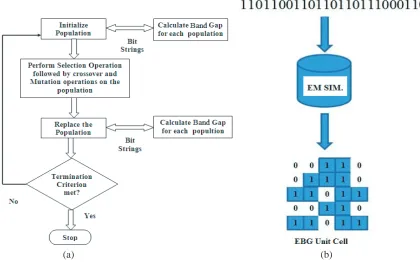
In the proposed optimization technique, a MATLAB based EM simulator employing useful inbuilt functions is developed which partly employs the techniques developed by Makarov [16], where Rao-Wilson-Glisson basis functions are used for solving the integral equations. The design of the structure is carried out using the PDE toolbox of MATLAB. This is combined with the GA to design the band gap structures with desired band gap characteristics. The flowchart for the GA/Method of Moments (MoM) based optimization of EBG structures is shown in Fig. 1(a). The GA generates the population whose chromosomes are binary bits. The GA then calls the MoM based simulator which generates the structure for the given input bit string, calculates the impedance matrix and finally provides the band gap for the given structure. If a bit is ‘1’ in the bit string, a metal patch is placed on the substrate at the given position, else no metal is placed. The coordinates are updated, and the process is repeated until all the bits in the bit string are used. Fig. 1(b) shows the EBG structure generated by the PDE tool box in MATLAB for a given input bit string, and the pseudo code for generating the optimized structure is shown below:
Pseudo Code for Band Gap Calculation: X=0;
Y =0;
for i=1: length (k) if (k (i) == 0)
Do not put metal on substrate; else
Place a square patch on substrate with length =5 mm; end
Update X and Y co-ordinates; end for;
Calculate the impedance matrix and calculate the 30 dB Band Gap
3. OPTIMIZED WIDE BAND EBG
(a) (b)
Figure 1. (a) Flow chart for GA/MoM based optimization. (b) Structure generation from an input bit string.
(a) (b) (c)
Figure 2. (a) Isometric view of the unit cell. (b) Top view of the prototype. (c) Bottom view of the prototype.
are fixed and are not part of the optimization process, such that the total number of chromosomes in each solution is 100. This particular dimension of 5 cm×5 cm is considered because of ease in fabrication. The parameters that have been taken for the GA are: No. of Chromosomes: 100; Population size: 20; Crossover rate: 0.35; Generations: 100; Mutation: Adaptive feasible.
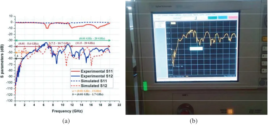
simulation results. TheS-parameters are shown in Fig. 3. The stopband characteristics of the EBG are listed in Table 1. The stopbands are measured at several isolation levels, such as −30, −40, −50 and −60 dB.
(a) (b)
Figure 3. S-parameters of the proposed optimized EBG structure. (a) Simulated values. (b) Measured values.
Table 1. Stop-band characteristics of proposed optimized unit EBG cell.
Isolation (dB) Stop-band range (GHz) Stop-band (GHz)
−30 0.01–20 20
−40 0.01–5.6 5.6
−40 7.2–10.7 3.5
−40 11.5–20 8.5
−50 0.01–3.0 3.0
−50 14.6–15.7 1.1
−60 0.01–1.7 1.7
From Fig. 3 it is observed that there is a good agreement between the measured and simulated results. The slight differences are due to the fabrication tolerances. Also, from the stopband characteristics in Table 1, the total band gap is found to be 20 GHz at −30 dB isolation, 17.4 GHz (5.6 GHz + 3.5 GHz + 8.5 GHz) at−40 dB isolation, 3 GHz at−50 dB isolation and 2.8 GHz (1.1 GHz + 1.7 GHz) at 60 dB isolation. Thus, the structure offers noise suppression over a wide band.
5. EYE DIAGRAM
A three-layer PCB stack-up as shown in Fig. 4 is considered for SI analysis, and the MEO and MEW are determined in two cases, one with the EBG power plane and the other without the EBG plane. The stacked configuration consists of a ground plane, an EBG power plane, and a signal layer (indicated by the checkered pattern in Fig. 4). The signal trace is on the signal layer which is placed at a height of 1.58 mm (thickness of the substrate) on top of the power plane. The SI analysis is performed on two reference boards, one with the EBG power plane and the other without the EBG power plane.
Figure 4. Isometric view of three layer PCB with EBG power plane.
The signal propagates on the top signal layer. This layer is placed on top of an FR4 Epoxy substrate having a height of 1.58 mm, dielectric constant of 4.4 and loss tangent of 0.02. This substrate is placed on top of the EBG power plane as shown in Fig. 4. The signal trace (indicated by the checkered pattern in Fig. 4) is designed as a 50 Ω line.
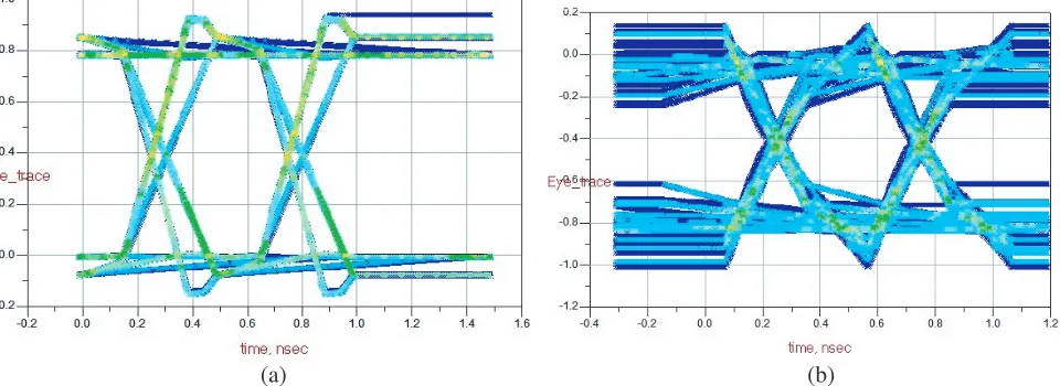
Two port S-parameters for the single ended traces are determined for the reference boards, one with EBG power plane and the other without the EBG power plane using MoM-based 2.5D solver IE3D. From the S-port parameters, the eye diagram is generated using Agilent’s Advanced Design Suite (ADS). A pattern of 27−1 pseudo random binary sequence (PRBS), non-return to zero (NRZ) coded at 2 GHz is launched at the input of port 1 to obtain the eye diagram. The signal is fed at the input (Port 1), and the eye pattern is monitored at the output (Port 2). The inserted PRBS is coded with a data rate having 1 V swing, and normalized rise/fall time is 200 ps. Figs. 5(a) and (b) show the eye patterns with and without the EBG configuration in the power plane.
(a) (b)
the PCB without EBG power plane, the degradations of the MEO and MEW of the PCB with single cell EBG power plane are about 10.5% and 2.8%, respectively. These values are comparable with the multi-slit EBG [10] where the MEO degradation is 16.2%, and MEW degradation is 1% for similar data conditions. This mild degradation is acceptable in high-speed circuits. A comparison of eye pattern parameters is shown for the proposed structure in Table 2.
Table 2. Comparison of proposed EBG cell with multi slit EBG.
Multi Slit EBG [10] Wide Band EBG [12] Proposed EBG
Without EBG power plane With EBG power plane Without EBG power plane With EBG power plane Without EBG power plane With EBG power plane MEO
(mV) 970 812 (16.2%) 899 772 (14.2%) 865 774 (10.5%)
MEW
(ns) 1980 1960 (1%) 500.4 500.3(0.02%) 503.2 489 (2.8%)
An overall comparison of all relevant parameters is shown in Table 3. The table gives a comparison of the stop band gap along with the SI analysis.
Table 3. Comparison of proposed EBG cell with other structures.
Parameters Proposed EBG Multi slit EBG [10] Wide Band EBG [12] LPC-EBG [6] Triangular Type [5] Double Square Ring [7] Isolation
level (dB) −30 −40 −50 −60 −50 −30 −40 −50 −30 −30
Band Gap
(GHz) 20 8.5 3 1.7 2.8 20 7.9 4.1 15 5
MEO Degradation
10.5% (2 Gbps) 2.1% (2.5 Gbps)
16.2% (2 Gbps)
14.2% (2 Gbps)
17%
(2.5 Gbps) N/A
19.2% (2.5 Gbps) MEW
Degradation
2.8% (2 Gbps) 14.1% (2.5 Gbps)
1% (2 Gbps)
0.02% (2 Gbps),
4.6%
(2.5 Gbps) N/A
5% (2.5 Gbps) Unit cell
dimensions (mm×mm)
50×50 65×32 55×40 30×30 30×30 30×30
6. CONCLUSION
REFERENCES
1. Wu, B., B. Li, T. Su, and C.-H. Liang, “Equivalent-circuit analysis and lowpass filter design of split-ring resonator DGS,” Journal of Electromagnetic Waves and Applications, Vol. 20, No. 14, 1943–1953, 2006.
2. Fu, Y. Q., Q. R. Zheng, Q. Gao, and G. H. Zhang, “Mutual coupling reduction between large antenna arrays using electromagnetic bandgap (EBG) structures,” Journal of Electromagnetic Waves and Applications, Vol. 20, No. 6, 819–825, 2006.
3. Senthinathan, R. and J. Price, “Simultaneous switching noise of CMOS, devices and systems,”
Springer International, 249, Kluwer, 1994.
4. Abhari, R. and G. V. Eleftheriades, “Metallo-dielectric electromagnetic bandgap structures for suppression and isolation of the parallel-plate noise in high-speed circuits,” IEEE Trans. Microw. Theory Technology, Vol. 51, No. 6, 1629–1639, 2003.
5. Kwon, J.-H., D.-U. Sim, S.-I. Kwak, and J. G. Yook, “Novel triangular-type electromagnetic bandgap structure for ultra-broadband suppression of simultaneous switching noise,”Microw. Opt. Technol. Letters, Vol. 51, 1356–1358, 2006.
6. Wu, T.-L., Y.-H. Lin, T.-K. Wang, C.-C. Wang, and S.-T. Chen, “Electromagnetic bandgap power/ground planes for wideband suppression of ground bounce noise and radiated emission in high-speed circuits,” IEEE Transactions on Microwave Theory and Techniques, Vol. 53, No. 9, 2935–2942, 2005.
7. Xu, X., J. Zhao, and Y. Feng, “Achieving both wideband mitigation of ground bounce noise and good signal integrity by novel period structure,”Electronics Letters, Vol. 45, No. 3, 158–159, 2009. 8. Rao, P. H. and M. Swaminathan, “A novel compact electromagnetic band gap structure in power plane for wideband noise suppression and low radiation,” IEEE Transactions on Electromagnetic Compatibility, Vol. 53, No. 4, 996–1004, 2011.
9. Rao, P. H., “Multi-slit electromagnetic band gap power plane for wideband noise suppression,”
IEEE Transactions on Components, Packaging and Manufacturing Technology, Vol. 1, No. 9, 1421– 1427, 2011.
10. Rao, P. H., “Hybrid electromagnetic Band gap power plane for ultra wideband noise suppression,”
Electronics Letters, Vol. 45, No. 19, 981–982, 2009.
11. Shi, L.-F., C.-R. Wang, S.-L. Yuan, K.-P. Chen, and S. Gao, “EBG structure with T-shaped slits for suppression of simultaneous switching noise,”International Journal of RF and Microwave Computer Aided Engineering, Vol. 25, 419–426, 2015.
12. Appasani, B. and N. Gupta, “A novel wide band-gap structure for improved signal integrity,”
International Journal of Microwave and Wireless Technologies, Vol. 8, No. 3, 591–596, 2016. 13. Pani, P., R. K. Nagpal, R. Malik, and N. Gupta, “Design of planar band Gap structures using
cuckoo search algorithm for ground noise suppression,”Progress In Electromagnetics Research M, Vol. 28, 145–155, 2013.
14. Pelluri, R. and B. Appasani, “Genetic algorithm optimized X-band absorber using metamaterials,”
Progress In Electromagnetics Research Letters, Vol. 69, 59–64, 2017.
15. Mosallaei, H. and K. Sarabandi, “A compact wideband EBG structure utilizing embedded resonant circuits,”IEEE Antennas and Wireless Propagation Letters, Vol. 4, No. 1, 5–8, 2005.