SOLAR ELECTRIC SYSTEM
ASMARASHID PONNIRAN
ABDUL FATAH MAT SAID
INTERNATIONAL CONFERENCE ON
INSTRUMENTATION, CONTROL & AUTOMATION
ICA 2009
DC-DC Boost Converter Design for Solar Electric System
Asmarashid Ponniran , A b d u l Fatah M a t Said
Faculty of Electrical and Electronic Engineering
Universiti Tun Hussein Onn Malaysia
86400 Parit Raja, Batu Pahat, Johor, M A L A Y S I A
E-mail: a s m a r @ u t h m . e d u . m y
Abstract
The main focus of this project is to design and construct a DC to DC converter (boost type) which is one of the main parts in solar electric system. Besides, to ensure that the output voltage will be step up from 12 V to 24 V. The 12 V input voltage is from the battery storage equipment and the 24 V output voltage will be the input of the inverter in solar electric system. In designing process, the switching frequency,/is set at 20 kHz and the duty cycle, D is 50%. The tool that been used for circuits simulation and validation are National Instrument Multisim software and OrCAD software. Then, all the parameter values that obtained from the hardware measurement are compared with the calculation estimation and the circuit simulation for validation purposes. Output of the project, 24 V regulated DC voltage is successfully met the requirement.
1 Introduction
This project is generally about a solar electric system for electrical appliances. Figure 1 shows the block diagram of the solar electric system. The main concern of this project is to design and construct a DC to DC converter which is one of the main module in the solar electric system that shown in Figure 1. The main idea of the DC to DC converter is based on boost type. The purpose of the project is to develop DC to DC converter (boost type) that converts the unregulated DC input to a controlled DC output with desired voltage level. The main objectives of this project are designing and constructing a DC to DC converter (boost type) circuit practically with input voltage, 12 V and the output voltage, 24 V.
Photovoltaic-Thermal (PV/T)
Module
Solar Charge Controller
Battery -Electric Energy
Storage
DC to DC Converter -BOOST
DC Load
AC Load
DC to AC Converter
Figure 1: Block diagram of Solar Electric System
2 Design Concept and Project Development
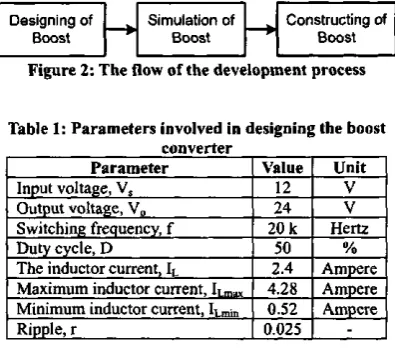
The main part of this project is DC to DC converter (boost type). This project consists of three main approaches of development process and that are design, simulate and construct. Figure 2 shows the flow of process in this project. Table 1 shows parameters involved in development of DC to DC converter (boost type).
Designing of Simulation of Constructing of
[image:2.594.308.506.535.710.2]Boost Boost Boost
Figure 2: The flow of the development process
Table 1: Parameters involved in designing the boost converter
Parameter Value Unit
Input voltage, Vs 12 V
Output voltage, V0 24 V
Switching frequency, f 20 k Hertz
Duty cycle, D 50 %
The inductor current, IL 2.4 Ampere
Maximum inductor current, IL m a x 4.28 Ampere
Minimum inductor current, IL m i n 0.52 Ampere
Ripple, r 0.025
I
If
V t « M 2 V 2 » 0
rt> * o <
TF» I s
0
Figure 3: The boost converter circuit design
Simulation Results
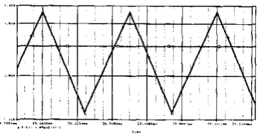
The circuit designed is simulated in National Instrument Multisim Power Pro Edition version 10 software or OrCAD versions 10.3 software. The designed that is simulated is the basic DC to DC converter (boos type). The inductor voltage and current output waveform for DC to DC converter (boost type) based on theory is shows in Figure 4.
The inductor current output waveform that obtained from the simulation is similar with the theoretical waveform. The output waveform that obtained is continuous conduction mode (CCM) which is the inductor current value greater than zero. Figure 6 shows the inductor current output waveform from simulation.
Figure 6: Inductor current output waveform from simulation
Figure 7 is the combination between inductor voltage and inductor current waveform. The waveform shows clearly the switching process.
Figure 7: The combination of inductor voltage and current output waveform
Figure 4: The inductor voltage and current waveform for boost converter (theory)
[image:3.594.313.497.190.287.2]For the simulation results of DC to DC converter (boost type) that designed, the inductor voltage output waveform from simulation is shown in Figure 5.
Figure 5: Inductor voltage output waveform from simulation
j
1;;
i1 i' 1 1 ' i
[ ; ! :
i 1 | ; 1
' ' 1 1 : i i
jl r i i i i: j
iai
•'ill . : ! , hFigure 8: The output waveform of boost converter circuit from simulation
Figure 8 shows the output waveform of the boost converter. The waveform is constant at 24.350 V.
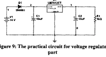
Voltage regulator part in the practical circuit
A voltage regulator is an electrical regulator designed to automatically maintain constantly voltage level. The maximum voltage from the battery is 13.8 V. The DC to DC converter (boost type) is step up from 12 V to 24 V. To 3 R e s u l t a n d A n a l y s i s
Circuit Design
[image:3.594.83.281.197.300.2] [image:3.594.92.274.576.676.2]Constructing of Practical Circuit
In developing and constructing process, the practical circuit that shows in Figure 11 is develops and construct.
w utnmt
[image:4.594.96.274.168.264.2]- V 1 - 1 4 V
Figure 9: The practical circuit for voltage regulator part
[image:4.594.302.509.177.279.2]For the simulation, the input voltage is 14 V and the output voltage that obtained is 11.960 V nearly to 12 V. Figure 10 shows the output voltage waveform of the voltage regulator from the simulation process.
Figure 11: The practical circuit for DC to DC converter (boost type)
The photograph of the hardware experimental setup is shown on Figure 12.
[image:4.594.85.520.324.480.2]tMkjiomijnv : M, j« W v - ( < a i , j j i r a v IB*. I T j y r " •> j j :
Figure 10: The voltage regulator output waveform from simulation
Table 2 shows the comparison parameter values between the calculation value and the simulation value.
Table 2: Comparison between calculation values with the simulation values
No Parameter Calculation
value
Simulation value
1 3.75 A 3.8558 A
2 -3.75 A -3.8558 A
3 Output voltage, V0 24 V 24.350 V 4 Inductor current, IL 2.4 A 3.4151 A
5 Max. inductor current, IL m a x
4.28 A 4.4361 A
6 Min. inductor current, IL m i n
0.52 A 0.562 A
7 Min. inductor, Lr a i n 75 uH 80 uH
8 Ripple, r 0.03
Figure 12: Hardware experimental setup Practical DC to DC Converter Testing and Calculation
Input and Output Voltage
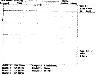
Figure 13 shows the input voltage waveform from the DC to DC converter (boost type) by the DL1620 digital oscilloscope and Figure 14 shows the output voltage waveform.
: K mi
AMD
[image:4.594.328.484.563.682.2]zi.y it
Figure 13: The input voltage waveform from the oscillation process
©2009 ICA, ISBN 978-979-8861-05-5 212
r~. f-~. n
'• AKUT
[image:5.594.101.269.121.255.2]STENT > S3 SAE&U
Figure 14: The output voltage waveform from the oscillation process
* ru.il K.JWKW r m « i r G.S
BNSCCLI ft •*.TJ*'
Figure 16: The PWM from pin 10 and pin 8
Table 3 shows the comparison parameter values between the calculations, simulation and practical output values.
Table 4 shows the comparison parameter values between the calculations, simulation and practical output values.
Table 3: Comparison between calculations, simulation and practical output values (using DL1620 digital
oscilloscope)
No Parameter Calculation value
Simulation value
Hardware value
1 Input voltage, Vs
12 V 12 V 12.9167 V
2 Output voltage, V0
24 V 24.350 V 24.5833 V
Pulse Width Modulation (PWM)
Figure 15 shows the diagram of integrated circuit (IC1 TDA2004).
+ Vs Bootstrap 1
Positive Input 1 1
Negative Input 1 2
Negative Input2 4
Positive Input 2 5
10 Output 1
8 Output 2
[image:5.594.326.486.125.242.2]Ground Bootstrap 2
Figure 15: IC1 TDA 2004 diagram
Based on Figure 15, pin 10 is output 1 and pin 8 is output 2. The output of pin 8 and pin 10 are a pulse width signals. Figure 16 shows the PWM from pin 10 and pin 8 obtained using DL1620 digital oscilloscopes.
Table 4: Comparison between calculations, simulation and practical output values (using DL1620 digital
oscilloscope)
No Parameter Calculation value
Simulation value
Hardware value
1 Duty
Cycle, D 5 0 % 5 0 % 33.33 %
Voltage Regulator Part
Voltage regulator is used in this practical circuit to maintain the voltage at 12 V from the charged battery that gives maximum output voltage 13.8 V. Figure 17 shows the output waveform form the voltage regulator. Table 5 shows the comparison between simulation and hardware values.
2*«W*'*X> to 46 61 :
[image:5.594.76.515.303.632.2]N*S(CLF UMFTW
[image:5.594.325.488.491.618.2]Table 5: Comparison between simulation and hardware values
No Parameter Simulation
value
Hardware value
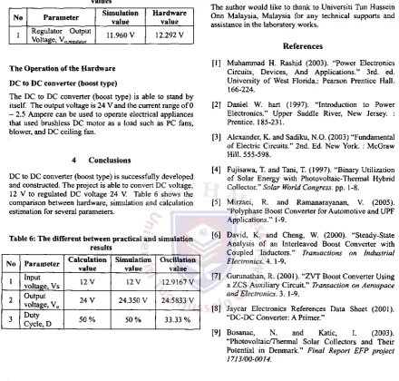
1 Regulator Output Voltage, V0.r e B U,a t o r
11.960 V 12.292 V
Acknowledgement
The author would like to thank to Universiti Tun Hussein Onn Malaysia, Malaysia for any technical supports and assistance in the laboratory works.
R e f e r e n c e s
The Operation of the Hardware
DC to DC converter (boost type)
The DC to DC converter (boost type) is able to stand by itself. The output voltage is 24 V and the current range of 0 - 2.5 Ampere can be used to operate electrical appliances that used brushless DC motor as a load such as PC fans, blower, and DC ceiling fan.
4 Conclusions
DC to DC converter (boost type) is successfully developed and constructed. The project is able to convert DC voltage, 12 V to regulated DC voltage 24 V. Table 6 shows the comparison between hardware, simulation and calculation estimation for several parameters.
Table 6: The different between practical and simulation results
No Parameter Calculation value
Simulation value
Oscillation value
1 Input
voltage, Vs 12V 12V 12.9167 V
2 Output voltage, V0
24 V 24.350 V 24.5833 V
3 Duty
Cycle, D 5 0 % 5 0 % 33.33 %
[1] Muhammad H. Rashid (2003). "Power Electronics Circuits, Devices, And Applications." 3rd. ed. University of West Florida.: Pearson Prentice Hall. 166-224.
[2] Daniel W. hart (1997). "Introduction to Power Electronics." Upper Saddle River, New Jersey. : Prentice. 185-231.
[3] Alexander, K. and Sadiku, N.O. (2003) "Fundamental of Electric Circuits." 2nd. Ed. New York. : McGraw Hill. 555-598.
[4] Fujisawa, T. and Tani, T. (1997). "Binary Utilization of Solar Energy with Photovoitaic-Thermal Hybrid Collector." Solar World Congress, pp. 1-8.
[5] Mirzaei, R. and Ramanarayanan, V. (2005). "Polyphase Boost Converter for Automotive and UPF Applications." 1-9.
[6] David, K. and Cheng, W. (2000). "Steady-State Analysis of an Interleaved Boost Converter with Coupled Inductors." Transactions on Industrial Electronics. 4. 1-9.
[7] Gurunathan, R. (2001). "ZVT Boost Converter Using a ZCS Auxiliary Circuit." Transaction on Aerospace and Electronics. 3. 1-9.
[8] Jaycar Electronics References Data Sheet (2001). "DC-DC Converter: A Primer."
[9] Bosanac, N. and Katie, I. (2003). "Photovoltaic/Thermal Solar Collectors and Their Potential in Denmark." Final Report EFP project 1713/00-0014.