Volume 2006, Article ID 75032, Pages1–13 DOI 10.1155/ASP/2006/75032
3D-SoftChip: A Novel Architecture for Next-Generation
Adaptive Computing Systems
Chul Kim,1Alex Rassau,1Stefan Lachowicz,1Mike Myung-Ok Lee,2and Kamran Eshraghian3
1Centre for Very High Speed Microelectronic Systems, Edith Cowan University, Joondalup, WA 6027, Australia
2School of Information and Communication Engineering, Dongshin University, Naju, Chonnam 520714, South Korea
3Eshraghian Laboratories Pty Ltd, Technology Park, Bentley, WA 6102, Australia
Received 1 October 2004; Revised 15 March 2005; Accepted 25 May 2005
This paper introduces a novel architecture for next-generation adaptive computing systems, which we term 3D-SoftChip. The 3D-SoftChip is a 3-dimensional (3D) vertically integrated adaptive computing system combining state-of-the-art processing and 3D interconnection technology. It comprises the vertical integration of two chips (a configurable array processor and an intelli-gent configurable switch) through an indium bump interconnection array (IBIA). The configurable array processor (CAP) is an array of heterogeneous processing elements (PEs), while the intelligent configurable switch (ICS) comprises a switch block, 32-bit dedicated RISC processor for control, on-chip program/data memory, data frame buffer, along with a direct memory access (DMA) controller. This paper introduces the novel 3D-SoftChip architecture for real-time communication and multimedia signal processing as a next-generation computing system. The paper further describes the advanced HW/SW codesign and verification methodology, including high-level system modeling of the 3D-SoftChip using SystemC, being used to determine the optimum hardware specification in the early design stage.
Copyright © 2006 Hindawi Publishing Corporation. All rights reserved.
1. INTRODUCTION
System design is becoming increasingly challenging as the complexity of integrated circuits and the time-to-market pressures relentlessly increase. Adaptive computing is a crit-ical technology to develop for future computing systems in order to resolve most of the problems that system design-ers are now faced with due in no small part to its potential for wide applicability. Up until now, however, this concept has not been fully realized because of many technology con-straints such as chip real-estate limitations and the software complexity. With the coupled advancement of semiconduc-tor processing technology and software technology, however, adaptive computing is now facing a turning point. For in-stance, the reconfigurable computing concept has more re-cently started to receive considerable research attention [1–3] and this concept is now starting to move and expand into the realm of adaptive computing. Software defined virtual hard-ware [4] and “do-it-all” devices [5] are good examples that demonstrate this development direction for computing sys-tems. The major forthcoming impact from the deployment of adaptive computing is do-it-all devices. For example, a small handheld PDA size device could assume the function-ality of about 10 standard devices simply depending on the context programs included such as a cellular phone, a GPS
receiver, an MP3 player, an e-book reader, a digital camera, a portable television, a satellite radio, a handheld gaming platform, and so forth. This concept also becomes increas-ingly important as there is a growing need for a single prod-uct to support multiple (and evolving) standards without re-engineering work.
Another growing problem in advanced computation sys-tems, particularly for real-time communication or video pro-cessing applications, is the data bandwidth necessary to sat-isfy the processing requirements. The interconnection wire requirements in standard planar technology are increasing almost exponentially as feature sizes continue to shrink. A novel 3D integration system such as 3D system-on-chip (SoC) [6], 3D-SoftChip [7, 8] which is able to satisfy the severe demand of more computation throughput by eff ec-tively manipulating the functionality of hardware primi-tives through vertical integration of two 2D chips is another concept proposed for next-generation computing systems. This paper proposes the novel 3D-SoftChip architecture as a forthcoming giga-scaled integrated circuit computing sys-tem and shows an implemented example of a single PE using SystemC.
Intelligent configuration switch (ICS)
Indium bump
interconnects Configurable array
processor (CAP)
Figure1: 3D-SoftChip physical architecture.
Data frame
buffer
Switch block Switch
block
Switch block
Switch block
Switch block
Switch block
Switch block
Switch block
Switch block
Switch block
Switch block
Switch block
Switch block
Switch block
Switch block
Switch block DMA
controller ICS
ICS
ICS
ICS
Memory Memory
P
rog
ra
m
m
emor
y
P
ro
gr
am
memor
y
Pro
gr
am
m
em
o
ry
Pro
gr
am
m
em
o
ry
PE
PE
PE
PE
PE
PE
PE
PE PE PE PE PE PE PE PE
PE PE PE PE PE PE PE
PE PE PE PE PE PE
Figure2: 3D-SoftChip: a novel 3D vertically integrated adaptive computing system-on-chip.
The lower chip is the configurable array switch (CAP). Inter-connection between the two 2D chips is achieved via an array of indium bump interconnections. A 2D planar architecture of the 3D-SoftChip can be seen inFigure 2.
The rest of the paper is organized as follows.Section 2 in-troduces an overview of the 3D adaptive computing system. Section 3provides overall explanations of the proposed 3D-SoftChip architecture and its distinctive features. Sections4 and 5 introduce the detailed architecture of the CAP and ICS chips, respectively. The interconnection network struc-ture is described inSection 6.Section 7describes a suggested HW/SW codesign and verification of the 3D-SoftChip and shows an implemented example of a single PE using Sys-temC. Finally, conclusions are provided inSection 8.
2. 3D ADAPTIVE COMPUTING SYSTEM
2.1. 3D vertically integrated systems overview
of 3D-SoC, 3D-SoftChip has been developed, which exploits the vertical integration of 2D planar chips to effectively ma-nipulate computation throughput. Previous work has shown that the 3D integration of systems has a number of benefits [10]. As described by Joyner et al. [10], 3D system integration offers a 3.9 times increase in wire-limited clock frequency, an 84% decrease in wire-limited area, or a 25% decrease in the number of metal levels required per stratum. There are three feasible 3D integration methods; a stacking of pack-ages, a stacking of ICs, and a vertical system integration as was introduced by IMEC [9]. In this research, however, the focus is on the use of indium bump interconnection technol-ogy as indium has good adhesion, a low contact resistance, and can be readily utilized to achieve an interconnect array with a pitch as low as 10µm. The development of 3D inte-grated systems will allow improvements in packaging costs, performance, reliability, and a reduction in the size of the chips.
2.2. Adaptive computing system
A reconfigurable system is one that has reconfigurable hard-ware resources that can be adapted to the application cur-rently under execution, thus providing the possibility to customize across multiple standards and/or applications. In most of the previous research in this area the concepts of re-configurable and adaptive computing have been described interchangeably. In this paper, however, these two concepts will be more specifically described and differentiated. Adap-tive computing will be treated as a more extended and ad-vanced concept of reconfigurable computing. Adaptive com-puting will include more advanced software technology to effectively manipulate more advanced reconfigurable hard-ware resources in order to support fast and seamless exe-cution across many applications. Table 1 shows the diff er-ences between reconfigurable computing and adaptive com-puting.
2.3. Previous work
Adaptive computing systems are mainly classified in terms of granularity, programmability, reconfigurability, computa-tional methods, and target applications. The nature of recent research work in this area according to these classifications, is shown inTable 2. This table shows that the early research and development was into single linear array-type reconfigurable systems with single and static configuration but also shows that this has evolved towards large adaptive SoCs with het-erogeneous types of reconfigurable hardware resources and with multiple and dynamic configurability.
As illustrated in Table 2, the 3D-SoftChip architecture has several superiorities when compared with conventional reconfigurable/adaptive computing systems resulting from the 3D vertical interconnections and the use of state-of-the-art adaptive computing technology (as will be described in the following sections). This makes it highly suitable for the next generation of adaptive computing systems.
3. 3D-SOFTCHIP ARCHITECTURE
3.1. Overall architecture of 3D-SoftChip
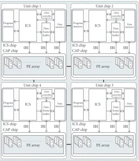
Figure 3shows the overall architecture of the 3D-SoftChip. As can be seen, it is comprised of 4 unit chips. By including four separate unit chips in the architecture, sufficient flexi-bility is provided to allow multiple optimized task threads to be processed simultaneously. Given the primary target appli-cations of multimedia processing and communiappli-cations four unit chips should be sufficient for all such requirements. Each unit chip has a PE array, a dedicated control proces-sor, and a high-bandwidth data interface unit. According to a given application program, the PE array processes large amounts of data in parallel while the ICS controls the overall system and directs the PE array execution, data, and address transfers within the system.
3.2. Features of 3D-SoftChip
The 3D-SoftChip has 4 distinctive features: various compu-tation models, adaptive word-length configuration computa-tion [7], optimized system architecture for communicacomputa-tion, and multimedia signal processing and dynamic reconfigura-bility for adaptive computing.
3.2.1. Computation algorithm: various computation models
As described before, one 32-bit RISC controller can supply control, data, and instruction addresses to 16 sets of PEs through the completely freely controllable switch block so various computation models can be achieved such asSISD, SIMD, MISD, and MIMD as required. Enough flexibility is thus achieved for an adaptive computing system. Especially, in the single instruction multiple data (SIMD) computation model, 3 types of different SIMD computational models can be realized, massively parallel, multithreaded, and pipelined [19]. In the massively parallel SIMD computation model, each unit chip operates with the same global program mem-ory. Every computation is processed in parallel, maximiz-ing computational throughput. In the multithreaded SIMD computation model, the executed program instructions in each unit chip can be different from the others so multi-threaded programs can be executed. The final one is the par-allel SIMD computation model. In this case each unit chip executes a different pipelined stage. Because of these SIMD computation characteristics, the 3D-SoftChip can adaptively maximize it’s computational throughput according to var-ious application requirements. These three computational models are illustrated inFigure 4.
3.2.2. Word-length configuration
Table1: Reconfigurable computing versus adaptive computing.
Reconfigurable computing Adaptive computing
Hardware resources Linear array of homogeneous elements (logic gates, lookup tables)
Heterogeneous algorithmic elements (complete function units such as ALU, multiplier)
Configuration Static, dynamic configuration, slow
reconfiguration time Dynamic, partial runtime reconfiguration
Mapping methods Manual routing, conventional ASIC design tools
(HDL) High-level language (SystemC,C)
Characteristics
Large silicon area, low speed (high capacitance), high-power consumption, high cost
Smaller silicon size, high speed, high performance, low-power consumption, low cost
Table2: Reconfigurable computing and adaptive computing systems.
System Granularity/
PE-type Programmability Reconfigurability
Computation
method Target application
PADDI [11] Coarse (16 bits) Multiple Static VLIW, SIMD DSP application
MATRIX [12] Coarse (8 bits) Multiple Dynamic MIMD General purpose
RaPiD [13] Coarse (16 bits) Single Mostly static Linear array Systolic arrays
Remarc [3] Coarse (16 bits) Multiple Static SIMD Data-parallel
RAW [14] Mixed Single Static MIMD General purpose
PipeRench [1] Mixed (128 bits) Multiple Dynamic Pipelined Data-parallel, DSP
MorphoSys [2] Coarse (16 bits) Multiple Dynamic SIMD Data-parallel
Triscend A7 [15] Mixed Multiple Dynamic N/A General purpose
Motorola MRC6011
[16] Coarse (16 bits) Multiple Dynamic SIMD
Computation intensive application QuickSilver
Adapt2400 [17]
Coarse
(8, 16, 24, 32 bits) Multiple Dynamic
Heterogeneous nodes array
Comm., multimedia DSP
Elixent DFA100 [4] Coarse (4 bits) Multiple Dynamic Linear D-fabric array
Multimedia applications PicoChip PC102
[18] Coarse (16 bits) Multiple Dynamic 3way-LIW Wirelesscommunications
3D-SoftChip Coarse (4 bits) Multiple Dynamic Various types ofcomputation models
Comm., multimedia signal processing
configuration algorithm. When 2 PEs configure together, an 8-bit word-length system is created. If 4 PEs configure to-gether this extends to 16 bits. And finally when 8 PEs con-figure together a full 32-bit word length is achieved. This flexibility is possible due to the configurable nature of the arithmetic primitives in the PEs [7,20] and the completely freely controllable switch block architecture in the ICS chip.
3.2.3. Optimized system architecture for communication and multimedia signal processing
There are many similarities between communications and multimedia signal processing, such as data parallelism, low-precision data, and high-computation rates. The different characteristics of communication signal processing are basi-cally more data reorganization, such as matrix transposition
and potentially higher bit-level computation. To fulfill these signal processing demands, each unit chip contains two types of PE. One is a standard PE for generic ALU functions, which is optimized for bit-level computation. The other is a pro-cessing accelerator PE for DSP. In addition, special address-ing modes to leverage the localized memory along with 16 sets of loop buffers in the ICS add to the specialized charac-teristics for optimized communication and multimedia sig-nal processing.
3.2.4. Dynamic Reconfigurability for Adaptive Computing
Unit chip 1
DMA controller
Program memory
P E
P E
P E P E
ICS
ICS chip
CAP chip IBI IBI IBI Data frame buffer
Data memory
PE array
Unit chip 2
DMA controller
Program memory
P E
P E
P E
P E
ICS
ICS chip
CAP chip IBI IBI IBI Data frame buffer
Data memory
PE array
Unit chip 4
DMA controller
Program memory
P E
P E
P E P E
ICS
ICS chip
CAP chip IBI IBI IBI Data frame buffer
Data memory
PE array
Unit chip 3
DMA controller
Program memory
P E
P E
P E
P E
ICS
ICS chip
CAP chip IBI IBI IBI Data frame buffer
Data memory
PE array
Figure3: Overall architecture for 3D-SoftChip.
indium bump interconnect array. Multiple sets of program memory, the abundant memory capacity, and the very high-bandwidth data interface unit makes it possible to switch programs easily and seamlessly, even at runtime.
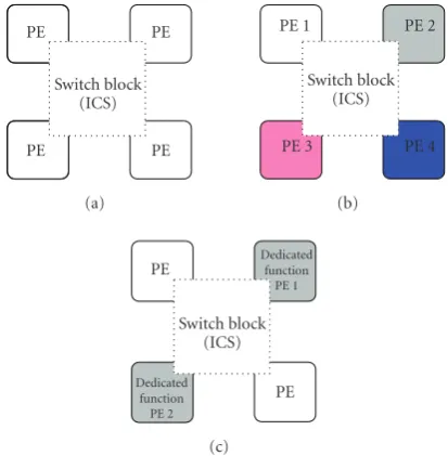
4. ARCHITECTURE OF CAP CHIP
The basic architecture of CAP chip is a linear array of het-erogeneous PEs.Figure 6shows three possible architecture choices for the PEs. The architecture in Figure 6(b)is sug-gested as the most feasible architecture for the PE in the 3D-SoftChip because it has the optimum tradeoffbetween application-specific performance and flexibility. Examples of type A can be seen in [1,2,12,14], type B in [17], and type C in [18]. The CAP chip has the basic role of the processing engine for the 3D-SoftChip. It manipulates large amounts of data at a high-computational rate using any of the three dif-ferent SIMD computation models previously described.
4.1. Two types of PEs
Figure 7illustrates the two types of PE architecture chosen to optimize multimedia signal processing and communication type applications.
4.1.1. Standard PE
The S-PE is for standard ALU functions and is also optimized for bit-level operation for communication signal processing. It comprises 4 sets of 19-bit registers for S-PE instruction decoding, two multiplexers to select input operands from the data bus, adjacent PEs, or internal registers; a standard ALU with a bit-serial multiplier, adder, subtracter, and com-parator, an embedded local SRAM and 4 sets of registers. The arithmetic primitives are scalable so as to make it pos-sible to reconfigure the word-length for specific tasks. The scalable arithmetic primitive’s architecture is presented in [7,20]. Moreover it can execute single-clock-cycle absolute value computation and comparison.Table 3shows the func-tions of S-PE. It is suitable for bit-wise manipulation and generic ALU functions.
4.1.2. Processing accelerator PE
Program 1 Program 1 Program 1 Program 1 DMA controller DMA controller DMA controller DMA controller P E P E P E P E P E P E P E P E P E P E P E P E P E P E P E P E ICS ICS ICS ICS PE array PE array PE array PE array ICS chip ICS chip ICS chip ICS chip
IBI IBI IBI IBI IBI IBI
IBI IBI IBI IBI IBI IBI
CAP chip CAP chip
CAP chip CAP chip Unit chip 1: program 1 execution
Unit chip 4: program 1 execution
Unit chip 2: program 1 execution
Unit chip 3: program 1 execution
Data frame buffer
Data frame buffer
Data frame buffer
Data frame buffer Data memory Data memory Data memory Data memory (a) Program 1 Program 2 Program 4 Program 3 DMA controller DMA controller DMA controller DMA controller P E P E P E P E P E P E P E P E P E P E P E P E P E P E P E P E ICS RISC ICS RISC ICS RISC ICS RISC PE array PE array PE array PE array ICS chip ICS chip ICS chip ICS chip
IBI IBI IBI IBI IBI IBI
IBI IBI IBI IBI IBI IBI
CAP chip CAP chip
CAP chip CAP chip Unit chip 1: program 1 execution
Unit chip 4: program 4 execution
Unit chip 2: program 2 execution
Unit chip 3: program 3 execution
Data frame buffer
Data frame buffer
Data frame buffer
Data frame buffer Data memory Data memory Data memory Data memory (b) Program 1 Program 2 Program 4 Program 3 DMA controller DMA controller DMA controller DMA controller P E P E P E P E P E P E P E P E P E P E P E P E P E P E P E P E ICS RISC ICS RISC ICS RISC ICS RISC PE array PE array PE array PE array ICS chip ICS chip ICS chip ICS chip
IBI IBI IBI IBI IBI IBI
IBI IBI IBI IBI IBI IBI
CAP chip CAP chip
CAP chip CAP chip Unit chip 1: pipeline stage 1
Unit chip 4: pipeline stage 4
Unit chip 2: pipeline stage 2
Unit chip 3: pipeline stage 3
Data frame buffer
Data frame buffer
Data frame buffer
Data frame buffer Data memory Data memory Data memory Data memory (c)
Figure4: Computation algorithm: 3 types of SIMD computation models. (a) Massively parallel SIMD computation model, (b) multi-threaded SIMD computation model, and (c) pipelined SIMD computation model.
and MAS operations within one clock cycle, an 8-bit con-figurable barrel shifter, an embedded local SRAM, and 4 sets of registers. Two shifters in the quad-PE can also be
PE PE PE PE PE PE PE PE
PE PE PE PE PE PE PE PE
(a)
PE PE PE PE PE PE PE PE
PE PE PE PE PE PE PE PE
(b)
PE PE PE PE PE PE PE PE
PE PE PE PE PE PE PE PE
(c)
Figure5: Word-length configuration algorithm. (a) 8-bit configu-ration, (b) 16-bit configuconfigu-ration, and (c) 32-bit configuration.
Switch block (ICS)
PE PE
PE PE
(a)
Switch block (ICS)
PE 1 PE 2
PE 3 PE 4
(b)
Switch block (ICS) PE Dedicatedfunction
PE 1
Dedicated function PE 2
PE
(c)
Figure6: Types of PEs: (a) homogeneous-type, (b) heterogeneous-type, and (c) heterogeneous-type with dedicated functions for spe-cial purpose.
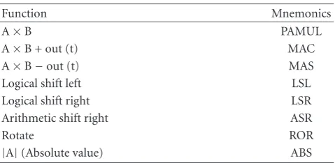
Table 4 describes the PA-PE functions, it is specialized for DSP operations such as MAC, MAS, logical shift, arithmetic shift, rotate, and absolute value computation.
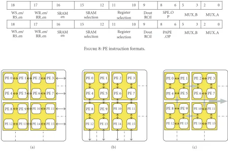
4.1.3. PE instruction format and operation modes
The PE instruction format consists of a 19-bit instruc-tion word. The MSB 2 bits (WS en/RS en,WR en/RR en) are
Data bus
Adjacent PEs Data bus Adjacent PEs ICS
MUX A MUX B
ALU (mul, add, sub, comp)
Register
Embedded SRAM Data bus
Data
In
st
ru
ct
io
n
d
ec
o
d
er
(a)
Data bus
Adjacent PEs Data bus Adjacent PEs ICS
MUX A MUX B
Multiplier (MAC, MAS)
Accumulator/subtractor
8-bit parallel shifter
Register
Embedded SRAM Data bus
Adjacent PEs
Data
In
st
ru
ct
io
n
d
ec
o
d
er
(b)
Figure7: Two types of PE: (a) standard PE and (b) processing ac-celerator PE.
used for the read/write enable bit of the embedded SRAM and registers. Bits 16 to 10 are used for SRAM and register selection (addressing). Bit 9 is used for data output register enable signal and bits 8 to 6 are used to specify the PE oper-ation. Finally, bits 5 to 0 are used to control the input multi-plexers for input operand selection. This format is illustrated inFigure 8below.
Table3: Standard PE functions.
Function Mnemonics
A and B AND
A or B OR
A xor B XOR
A + B ADD
A−B SUB
A×B SPMUL
A comp B COMP
|A|(Absolute value) ABS
Table4: Processing accelerator PE functions.
Function Mnemonics
A×B PAMUL
A×B + out (t) MAC
A×B−out (t) MAS
Logical shift left LSL
Logical shift right LSR
Arithmetic shift right ASR
Rotate ROR
|A|(Absolute value) ABS
flexibility and help to maximize computational throughput according to the target application.
4.2. Embedded local SRAM
Each PE has a local embedded SRAM. The effective memory bandwidth is, therefore, increased dramatically by as much as the total number of PEs, which will result in an increase in effective processing speed in many applications and allows for rapid dynamic context switching. Bus traffic can also be reduced because many data transmission operations can be contained within a PE. Consequently, power dissipation will also be minimized.
4.3. Quad-PE
As previously described one quad-PE consists of two pairs of PEs (two S-PE and two PA-PE). The quad-PE is controlled and configured by the switch block according to the control and address data from the ICS transmitted through the IBIA. Figure 10shows the architecture of a single quad-PE.
5. ARCHITECTURE OF ICS CHIP
The ICS chip comprises the switch blocks, ICS RISC, pro-gram memory, data memory, data frame buffers, and DMA controller as illustrated inFigure 11. The ICS chip is a control processor which controls the CAP chip via the IBIA as well as the overall system. The ICS RISC provides control and ad-dress signals and data to the system as a whole. The switch blocks configure each PE based on the current program in-struction. The high-bandwidth data interface unit enables ef-ficient transmission of data and instructions within the sys-tem.
5.1. Switch block
The switch block provides data from/to each PE and also provides instruction data to each PE. Three types of switch blocks, 6-sided, 7-sided, and 8-sided, provide optimized in-terconnections within the ICS chip. A pass-transistor design is used to optimize performance and minimize area allowing a completely free configuration for each PE.
5.2. ICS RISC
The ICS RISC is a 32-bit dedicated RISC control processor. The ICS RISC controls the execution of the PE array and provides control and address signals to program/data mem-ory, the data frame buffers, and the DMA controller. It has a 3-stage pipelinedarchitecture that includes instruction fetch (F), decode (D), and execute (E). To cope with the iterative nature of DSP arithmetic, it also has 16 sets of loop buffers so as to provide direct instruction to instruction decoding in-stead of fetching from program memory in each case. This significantly reduces bus utilization allowing for improved performance and lower-power dissipation. Moreover 32 gen-eral purpose registers and specialized addressing modes are provided for optimized communication and multimedia sig-nal processing.
5.3. High-bandwidth data interface unit
The high-bandwidth data interface unit allows the efficient transfer of data within the 3D-SoftChip. Two sets of data frame buffers and the DMA controller make it easy to trans-fer large amounts of data. Multiple sets of program memory support runtime program switching and, because of this dy-namic reconfiguration feature, adaptive computing is possi-ble. The data memory has a variable word width so it can eas-ily be combined to build wider/deeper memories and thus in-crease flexibility for different application programs andmul-tiple word-length computations.
6. INTERCONNECTION NETWORK
Register selection WS en/
RS en
WR en/
RR en SRAMen
SRAM selection
Dout RCtl
SPE O
P MUX B MUX A
18 17 16 15 12 11 10 9 8 6 5 3 2 0
Register selection WS en/
RS en
WR en/ RR en
SRAM
en selectionSRAM DoutRCtl PAPEOP MUX B MUX A
18 17 16 15 12 11 10 9 8 6 5 3 2 0
Figure8: PE instruction formats.
PE 0 PE 1 PE 2 PE 3
PE 4 PE 5 PE 6 PE 7
PE 8 PE 9 PE 10 PE 11
PE 12 PE 13 PE 14 PE 15
(a)
PE 0 PE 1 PE 2 PE 3
PE 4 PE 5 PE 6 PE 7
PE 8 PE 9 PE 10 PE 11
PE 12 PE 13 PE 14 PE 15
(b)
PE 0 PE 1 PE 2 PE 3
PE 4 PE 5 PE 6 PE 7
PE 8 PE 9 PE 10 PE 11
PE 12 PE 13 PE 14 PE 15
(c)
Figure9: PE operation modes: (a) horizontal mode, (b) vertical mode, and (c) circular mode.
it supports a very high bandwidth coupled with a very low inductance/capacitance (and thus low-power dissipation) [8]. However, any other equivalent 3D-interconnection tech-nology could also be applied to realize this interconnection level within the 3D-SoftChip architecture.
6.1. Indium bump interconnection
Indium is an excellent material to use as an interconnect ma-terial due to its excellent adhesion to most metals, includ-ing aluminum, which is the metallization for the pads used in most VLSI technologies. Indium has a low melting point, which implies a low work-hardening coefficient, allowing for direct bonding on processed VLSI wafers. Additionally, it provides excellent mechanical as well as electrical connectiv-ity (contact resistance<1 mΩper bump). Reflow techniques can be used for flexibility and to increase the bump height to width ratio as needed. Such techniques can also be used to incorporate self-alignment features to the bonding pro-cess.Figure 12(a)illustrates a cut-away view of the flip-chip indium bump interconnection, a micrograph of a single in-dium bump after reflow can be seen inFigure 12(b).
7. HW/SW CODESIGN AND VERIFICATION METHODOLOGY
Figure 13 shows the HW/SW codesign methodology for the 3D-SoftChip. HW/SW partitioning is being executed to
determine which functions should be implemented in hard-ware and which in softhard-ware. The HW is currently being mod-eled at a system level using SystemC [21,22] to verify func-tionality of the operation and to explore various architec-ture configurations while concurrently modeling the soft-ware in C. After that, a cosimulation and verification process will be implemented to verify the operation and performance of the 3D-SoftChip architecture and to decide on an opti-mal HW/SW architecture. More specifically, the SW will be a modified GNU C Compiler and Assembler. After the com-piler and assembler for ICS RISC has been finalized, a pro-gram for the implementation of the MPEG4 motion estima-tion algorithm will be developed and compiled using it. Af-ter that, object code can be produced, which can be directly used as the input stimulus for an instruction set simulator and system level simulation. The HW/SW verification pro-cess can be achieved through the comparison between the re-sults from instruction-level simulation and system-level sim-ulation. From this point on, the rest of the procedure can be processed using any conventional HW design methodology, such as full and semicustom design.
7.1. System level modeling of single PE
Data bus Adjacent PEsData bus Adjacent PEs
ICS
Inter PE bus
MUX A MUX B
ALU (mul, add, sub, comp)
Inter PE bus Embedded SRAM Data bus
Address
In
st
ru
ct
io
n
d
ec
o
d
er
Data bus Adjacent PEs Data bus
ICS
MUX A M
ALU (mul, add, sub, comp)
Embedded SRAM Data bus
Address
Register
In
st
ru
ct
io
n
d
ec
o
d
er
Data bus
Adjacent PEsData bus Adjacent PEs
ICS
MUX A MUX B
Multiplier (MAC, MAS)
Accumulator/subtractor
8-bit parallel shifter
Register
Embedded SRAM
ctio
n
d
ec
od
er
Inter PE bus
Adjacent PEs Data bus Adjacent PEs
UX A MUX B
Multiplier (MAC, MAS)
Accumulator/subtractor
8-bit parallel shifter
Register
Embedded SRAM
In
st
ru
Data bus Adjacent PEs
Data
Address
Inter PE bus Switch block Metalization pad
IBI
IBI
IBI
IBI
IBI
IBI
IBI
IBI
Figure10: Quad PE.
Instruction address 31 : 0
Instruction address 31 : 0
Loop buffer (16×32 bit)
Register file (32×32 bit) Program counter
I/O unit
Instruction data<31 : 0>
Instruction register
ALU & control unit
Control signals ICS RISC
· · ·
Subtrate/CAP chip
ICS chip Indium bumps
Bonding pad
(a) (b)
Figure12: (a) 3D flip-chip indium bump interconnection and (b) indium bump interconnection: single indium bump after reflow.
HW/SW partitioning 3D-SoftChip system specification
System-level modeling & architecture exploration of 3D-SoftChip using SystemC
Possible design specifications H/W
*SystemC modeling system-level modeling for function/instruction verif.
& arch. exploration ICS compiler
assembler design (modify GUN C compiler/
assembler)
Program coding, assembling (ICS assembler)
Instruction-level simulation (ICS instruction set
simulator) S/W
S/W specification
System-level simulation
Design verification result checking
Optimum H/W specifications
Layout/ circuit-level simulation
layout editor, spice Circuit optimization
Design verification
DRC, LVS Go to foundry Chip test
Circuit optimization
HW/SW codesign
Object codes
HW/SW coverification
ILS results
SLS results
Reset
Din
Instructions
Clock
Dout
Clock Stimulus
Standard PE
(a)
Testbench.cpp decoder.cppInstruction ALU.cpp SRAM.cpp
Testbench.h Instructiondecoder.h ALU.h SRAM.h
Main.cpp SystemC.h
(b)
(c)
Figure14: System level modeling of single PE: (a) standard PE block diagram, (b) file structure of standard PE, and (c) the output waveform of system-level modeled standard PE.
8. CONCLUSIONS
A novel 3D vertically integrated adaptive computing system architecture for communication and multimedia signal pro-cessing has been presented along with system-level model-ing example of a smodel-ingle PE. The described system leverages the very high-bandwidth connection between two chips, re-alizable through the indium bump interconnect array, to combine high-level ICS and low-level CAP processing en-gines to create a next-generation adaptive computing sys-tem. The described system architecture of the 3D-SoftChip is currently being fully modeled in SystemC in order to de-termine the optimal hardware architecture. The SW design is being concurrently finalized so that the novel concept of an adaptive system-on-chip computing system can be real-ized.
REFERENCES
[1] S. C. Goldstein, H. Schmit, M. Budiu, S. Cadambi, M. Moe, and R. R. Taylor, “PipeRench: a reconfigurable architecture and compiler,”IEEE Computer, vol. 33, no. 4, pp. 70–77, 2000. [2] H. Singh, M.-H. Lee, G. Lu, F. J. Kurdahi, N. Bagherzadeh, and E. M. Chaves Filho, “MorphoSys: an integrated reconfigurable system for data-parallel and computation-intensive applica-tions,”IEEE Transactions on Computers, vol. 49, no. 5, pp. 465– 481, 2000.
[3] T. Miyamori and K. Olukotun, “REMARC: reconfigurable multimedia array coprocessor,” inProceedings of ACM/SIGDA 6th International Symposium on Field Programmable Gate
Ar-rays (FPGA ’98), pp. 261–261, Monterey, Calif, USA, February
1998.
[4] Elixent Limited, “The Reconfigurable Algorithm Processor,”
[5] N. Tredennick and B. Shimamoto, “Special Report: do-it-all devices,”IEEE Spectrum, pp. 37–40, December 2003.
[6] J. W. Joyner, P. Zarkesh-Ha, and J. D. Meindl, “Global in-terconnect design in a three-dimensional system-on-a-chip,”
IEEE Transactions on Very Large Scale Integration (VLSI) Sys-tems, vol. 12, no. 4, pp. 367–372, 2004.
[7] S. Eshraghian, S. Lachowicz, and K. Eshraghian, “3-D verti-cally integrated configurable soft-chip with terabit computa-tional bandwidth for image and data processing,” in Proceed-ings of 10th International Conference on Mixed Design of
Inte-grated Circuits and Systems (MIXDES ’03), pp. 143–148, Lodz,
Poland, June 2003.
[8] A. Rassau, G. Alagoda, A. Ehrhardt, S. Lachowicz, and K. Eshraghian, “Design methodology for a 3D softchip video processing architecture,” inProceedings of 6th World
Multicon-ference on Systemics, Cybernetics and Informatics (SCI ’02), pp.
324–329, Orlando, Fla, USA, July 2002.
[9] IZM, “3D System Integration,” http://www.pb.izm.fhg.de/ izm/015 Programms/010 R/.
[10] J. W. Joyner, R. Venkatesan, P. Zarkesh-Ha, J. A. Davis, and J. D. Meindl, “Impact of three-dimensional architectures on interconnects in gigascale integration,”IEEE Transactions on
Very Large Scale Integration (VLSI) Systems, vol. 9, no. 6, pp.
922–928, 2001.
[11] D. Chen and J. Rabaey, “PADDI: programmable arithmetic devices for digital signal processing,” inProceedings of IEEE
Workshop on VLSI Signal Processing, pp. 240–249, IEEE Press,
San Diego, Calif, USA, November 1990.
[12] E. Mirsky and A. DeHon, “MATRIX: a reconfigurable com-puting architecture with configurable instruction distribution and deployable resources,” inProceedings of IEEE Symposium
on FPGAs for Custom Computing Machines, pp. 157–166, Napa
Valley, Calif, USA, April 1996.
[13] D. C. Cronquist, C. Fisher, M. Figueroa, P. Franklin, and C. Ebeling, “Architecture design of reconfigurable pipelined dat-apaths,” inProceedings of 20th Anniversary Conference on
Ad-vanced Research in VLSI (ARVLSI ’99), pp. 23–40, Atlanta, Ga,
USA, March 1999.
[14] E. Waingold, M. Taylor, D. Srikrishna, et al., “Baring it all to software: raw machines,”IEEE Computer, vol. 30, no. 9, pp. 86–93, 1997.
[15] Triscend Corporation, “Triscend A7S Configurable System-on-Chip Platforms,”http://www.triscend.com.
[16] Motorola Incorporation, “MRC6100: Reconfigurable Com-pute Fabric (RCF) device,” http://www.motorola.com/semi-conductors/.
[17] QuickSilver Technology Incorporation, “Adapt2400 ACM Ar-chitecture Overview”.
[18] picoChip Designs Limited, “PC102 Product Brief,” http:// www.picochip.com.
[19] L. Guangming,Modeling, implementation and scalability of the
morphoSys dynamically reconfigurable computing architecture,
Ph.D. thesis, Electrical and Computer Engineering Depart-ment, University of California, Irvine, Calif, USA, 2000. [20] S. Eshraghian, “Implementation of arithmetic primitives
us-ing truly deep submicron technology (TDST),” Ms thesis, Edith Cowan University, Perth, Australia, 2004.
[21] Open SystemC Initiative, “The Functional Specification for SystemC 2.0,”http://www.systemc.org/.
[22] Open SystemC Initiative, “SystemC 2.0.1 Language Reference Manual Rev 1.0,”http://www.systemc.org/.
Chul Kimreceived the B.S. degree in elec-tric engineering from Sunchon National University, Korea, in 2003. He is currently pursuing his Masters degree at the Center for Very High Speed Microelectronic Sys-tems, Edith Cowan University, Perth, Aus-tralia. His research interests include 3D adaptive computing systems and platform-based SoC design for communication and multimedia signal processing.
Alex Rassaureceived a Ph.D. degree in mi-croelectronics from the University of Read-ing, ReadRead-ing, England in 2000. He joined the Centre for Very High Speed Microelec-tronic Systems at Edith Cowan University in 2000 and his current research interests in-clude new adaptive computing architectures and microphotonic systems.
Stefan Lachowicz received M.Eng.Sc. and Ph.D. degrees from the Technical Univer-sity of Lodz, Poland in 1982 and 1987, re-spectively. In 1993 he joined Edith Cowan University as a Senior Lecturer in engineer-ing at the School of Engineerengineer-ing and Math-ematics and the Deputy Director of The National Networked Teletesting Facility for Integrated Systems (NNTTF). His research interests include CMOS imagers, reconfig-urable architectures, and design for test.
Mike Myung-Ok Leereceived B.S., MNS, and Ph.D. degrees from the Arizona State University, Tempe, U.S.A. in 1983, 1987, and 1988, respectively. He is a Professor in the School of Informa-tion and CommunicaInforma-tion Engineering, Dongshin University, Ko-rea, and his current research interests include high-speed intelligent network design, multimedia Optic-VLSI/ULSI design, telecommu-nication engineering, and nanobio-medical engineering.
Kamran Eshraghian received B.Tech., M.Eng.Sc., and Ph.D. degrees from the Uni-versity of Adelaide, South Australia. In 1979 he joined the Department of Elec-trical & Electronic Engineering at the University of Adelaide after spending 10 years with Philips Research both in Europe and Australia. He has held a number of visiting academic posts including Professor of Computer Science at Duke University,