Vol. 4, Issue 9, September 2015
Low power High performance adder with
Prefix Tree Structure configuration
Venkata K. Ramanaiah
Associate Professor, Dept. of ECE, YSR Engineering College of Yogi Vemana University, Proddatur, Andhra Pradesh, India
ABSTRACT: In the advancements of modern technology the field of nanometer technology makes to maximize the speed performance and minimize the power of logic designs particularly in the binary arithmetic digital design stream. This can be achieved by Parallel Prefix Tree Structure. Proposed design investigates a 64-bit hybrid digital adder circuit by using radix-4 tree structure and carry select adder. As the design is imposed with carry select, the carry propagation time is reduced. The proposed design have designed and simulated using verilog hardware description language (HDL) using Xilinx Integrated Software Environment (ISE) 14.3 Design Suite. These designs are implemented in Xilinx Field Programmable Gate Arrays. The experimental results proved that the proposed 64-bit hybrid adder is superior to other adders, and has 2.71ns delay time, 9.58 mw average power.
KEYWORDS: Carry select adder, FPGA, hybrid adder, low power, parallel prefix adder
I.INTRODUCTION
The binary addition is the basic arithmetic operation in any digital circuit and it becomes essential in most of the digital systems including arithmetic and logic unit (ALU), microprocessors, digital signal processing (DSP) and floating point unit (FPU). With the rapid growth in portable electronic equipments and mobile communication devices, demand to low voltage and low power technology for VLSI applications is great increasing. In general, high speed adder includes carry look ahead adder (CLA), carry select adder (CSA), carry bypass adder (CBA), conditional sum adder and later developed parallel prefix adder (PPA). Different prefix algorithms and tree topologies (BKA, STA, KSA, SKA) of PPAs have been implemented for solving delay, area, and power efficiencies. Design of an appropriate tree topology is a trade-off among the fan-out, the wiring count and the logic level [1]. Recently, several high-performance 64-bit adders have been reported in [2-3]. The high-speed 64-bit adder [2] is hybrid sparse radix-4 prefix tree and CSA based on energy-delay optimization methodology. In this paper, a 64-bit hybrid adder is proposed to combine both prefix tree structure (PTS) and CSA for fetching low voltage and low power features. The three stages prefix tree of the 64-bit hybrid adder computes carries, and then the CSA with add-one circuit selects sums by these carries. Otherwise, the CBA has been added at the third stage of the PTS to diminish fan-ins, fan-outs, wiring counts and transistor counts. With respect to low voltage low power method, complementary metal oxide semiconductor (CMOS) logic, transmission gate (TG) logic, and pass transistor logic (PTL) are applied in proposed design to fetch full swing operation at each node.
II. EXISTING SYSTEM
ISSN (Print) : 2320 – 3765 ISSN (Online): 2278 – 8875
I
nternational
J
ournal of
A
dvanced
R
esearch in
E
lectrical,
E
lectronics and
I
nstrumentation
E
ngineering
(An ISO 3297: 2007 Certified Organization)
Vol. 4, Issue 9, September 2015
In order to reduce the delay in RCA (or) to propagate the carry in advance, we go for carry look ahead adder .Basically this adder works on two operations called propagate and generate. The propagate and generate equations are given by.
Pi=Ai XOR Bi (1)
G i= Ai AND Bi (2)
For 4 bit CLA, the propagated carry equations are given as
C 1G 0P 0 C 0 (3)
C 2G 1P 1 G0P 1 P 0C0 (4)
C3G2P 2G1P 2P1 G0P2 P1 P0C0 (5)
C4G3P3G2P3P2 G1P3P2P1G0P3 P2 P1 P0 C0 (6)
Equations (3), (4), (5) and (6) are observed that, the carry complexity increases by increasing the adder bit width. So designing higher bit CLA becomes complexity. In this way, for the higher bit of CLA’s, the carry complexity increases by increasing the width of the adder. So results in bounded fan-in rather than unbounded fan-in, when designing wide width adders. In order to compute the carries in advance without delay and complexity, there is a concept called Parallel prefix approach.
The PPA’s pre-computes generate and propagate signals are presented in [4]. Using the fundamental carry operator, these computed signals are combined in [5].The fundamental carry operator is denoted by the symbol “”,
(gL, pL) o( gR ,pR) = (gL+ pL .g R , p L , p R) (7) For example, 4 bit CLA carry equation is given by,
C4g4, p4)g3, p3)o[(g4, p4) g3, p3)]] (8) For example, 4 bit PPA carry equation is given by,
C4g 4, p4)g 3, p3)]o[(g4, p4) g3, p3)] (9)
From equations (8) and (9) it is clear that, the CLA takes three steps to generate the carry, but PPA takes two steps to
generate the carry.
Vol. 4, Issue 9, September 2015
Fig.3:Black and Gray cells
Fig.4:16-bit Sparse KoggeStone adder
PPA’s basically consists of three stages during addition process. They are
ISSN (Print) : 2320 – 3765 ISSN (Online): 2278 – 8875
I
nternational
J
ournal of
A
dvanced
R
esearch in
E
lectrical,
E
lectronics and
I
nstrumentation
E
ngineering
(An ISO 3297: 2007 Certified Organization)
Vol. 4, Issue 9, September 2015
Figure 3 shows the definitions of cells that are used in prefix structures, including BC and GC. For analysis of various parallel prefix structures, see [4], [5] & [6].
Kogge Stone Adder (KSA)
KSA is another of prefix trees that use the fewest logic levels. A 16-bit KSA is shown in Figure 6. The 16 bit kogge stone adder uses BC’s and GC’s and it won’t use full adders. The 16 bit KSA uses 36 BC’s and 15 GC’s. And this adder totally operates on generate and propagate blocks. So the delay is less when compared to the previous SKA and STA. The 16 bit KSA is shown in figure 4.In this KSA, there are no full adder blocks like SKA and STA [7] & [8].
III.PROPOSED 64-BIT HYBRID ARCHITECTURE
The figure 5 shows new hybrid adder, is constructed with three modules, which consists of Generate or Propagate Generation (GPG), Prefix Tree Structure (PTS) and the CSA with add-one circuit. The initial stage or starting stage of the GPG generates individual generate and propagate signals for each bit position. The middle stage of the PTS computes some specific carries to the next stage for the CSA. The final stage of the CSA with add-one circuit selects the proper sum as the output. It is advantages that the initial stage of sharing generates and propagates signals in both PTS and CSA blocks to reduce the hardware structure overheads to achieve more compact area with less leakage power.
Fig.5: Block diagram of proposed hybrid architecture
In PPA, the carry computation approach dominates the overall performance of the adder design. In order to fetch faster computation, lot of parallel prefix tree structure topologies have been designed and developed to have a good trade-offs between speed, power and area. The more efficient way is implementing parallelizable prefix computation by taking advantage of the associative operator “o” [9], 0].The generate (g) and propagate (p) signals can be defined as follow:
(g, p) o (g’, p’) = (g + pg’ pp’) (10)
Giving a series of bits i…j…k, the group generate/propagate pair (g i:k , p i:k) can be expressed in terms of input signals p j and g j from bit position i to k, respectively. Therefore,
Vol. 4, Issue 9, September 2015
Fig.6: Proposed 64-bit hybrid adder
The invented 64 bit hybrid adder has designed based on PTS and CSA, has shown in Figure 6. For a group of four bits, the radix-4, 64-bit hybrid adder is composed of three stages. According to the relationship between stage and radix in a prefix tree [2],[11],[12] the fewer stages depend on higher radix adopted, and the least stages are applied in prefix adder results in the potential higher speed and lowest power consumption. A 4-bit CSA is taken in my consideration is due to the delay time of a 4-bit carry ripple adder (CRA) module is slightly less than that of PTS. Consequently, every four-bit of PTS computes a carry for Corresponding 4-bit CSA module. To achieve the goal of high speed adder, carry-in signal (cin) directly connects to the second stage. The proposed structure differs greatly from other architectures in which carry-in signal are linked to the first stage. In such scheme, the critical path of proposed design has reduced load capacitance. As a result,the total performance of the adder will be boosted.
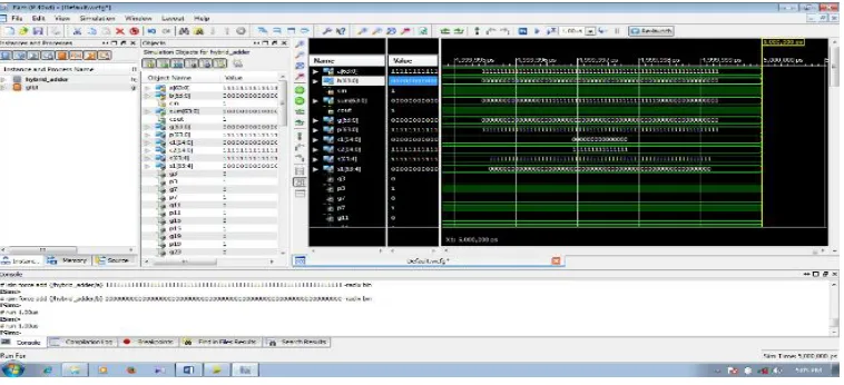
In the proposed 64-bit hybrid adder, the generate signal (gi) and propagate signal (pi) are generated at the initial stage. The radix-4 PTS, the middle stage, computes carries tothe CSA modules in final stage. For the first and second stages, every module utilizes CMOS logic to complete the intermediate carry. To diminish the fan-out at the second stage as the fan-in at the third stage, CBA is adopted at the third stage for terminal carry output. This turns out to greatly reduce the wiring counts, so the third stage owns compact area and lower power consumption. And CBAs skip over long carry ripple to reduce the delay time with fewer transistor numbers. At the final stage, the 4-bit CSA quickly produce sums through MUXs when carry signal arrived. Fig. 7 shows the simulated waveforms, and table 1 gives comparison of various adders.
ISSN (Print) : 2320 – 3765 ISSN (Online): 2278 – 8875
I
nternational
J
ournal of
A
dvanced
R
esearch in
E
lectrical,
E
lectronics and
I
nstrumentation
E
ngineering
(An ISO 3297: 2007 Certified Organization)
Vol. 4, Issue 9, September 2015
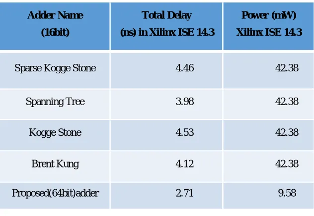
Table. 1. Comparison of adders
VI.CONCLUSION
The proposed hybrid adder is composed of the radix-4 prefix tree structure and the CSA to benefit the high speed. The experimental results show that the proposed 64-bit hybrid adder has 2.71ns delay, consumes 9.58mw power and utilization of lower look at tables (LUTs). As results, the design achieves superior power, speed, and area constraints and therefore this adder efficient and plays a crucial role in Processors, and arithmetic and logic operations etc., compared with other existing designs.
REFERENCES
[1] D. Harris, “A Taxonomy of Parallel Prefix Networks,” Conference Record of the Thirty-Seventh Asilomar Conference on Signals, Systems and Computers, vol. 2, pp. 2213-2217, 9-12 Nov. 2003
[2] R. Zlatanovici, S. Kao and B. Nikolic, “Energy–Delay Optimization of 64-Bit Carry-Lookahead Adders With a 240 ps 90 nm CMOS Design Example,” IEEE Journal of Solid-State Circuits, vol. 44, no. 2, pp. 569-583, Feb. 2009.
[3] Neve, H. Schettler, T. Ludwig and D. Flandre,“Power-Delay-product Minimization in High-Performance 64-bit Carry-Select Adders,” IEEE Transactions on Very Large Scale Integration (VLSI) Systems, vol. 12, no. 3, pp. 235-244, Mar. 2004.
[4] N. H. E. Weste and D. Harris, CMOS VLSI Design, 4th edition,Pearson–Addison-Wesley, 2011.
[5] R. P. Brent and H. T. Kung, “A regular layout for parallel adders,” IEEETrans. Comput., vol. C-31, pp. 260-264, 1982.
[6] D. Harris, “A Taxonomy of Parallel Prefix Networks,” in Proc. 37thAsilomar Conf. Signals Systems and Computers, pp. 2213–7, 2003. [7] P. M. Kogge and H. S. Stone, “A Parallel Algorithm for the EfficientSolution of a General Class of Recurrence Equations,” IEEE Trans.
OnComputers, Vol. C-22, No 8, August 1973.
[8] D. Gizopoulos, M. Psarakis, A. Paschalis, and Y. Zorian, “EasilyTestable Cellular Carry Lookahead Adders,” Journal of ElectronicTesting: Theory and Applications 19, 285-298, 2003.
[9] T. Lynch and E. E. Swartzlander, “A Spanning Tree Carry LookaheadAdder,” IEEE Trans. on Computers, vol. 41, no. 8, pp. 931-939, Aug.1992.
[10] R. P. Brent and H. T. Kung, “A Regular Layout for Parallel Adders,” IEEE Transactions on Computers, vol. C-31, no. 3, pp. 260-264, Mar. 1982.
[11] B. R. Zeydel, D. Baran and V. G. Oklobdzija, “Energy-Efficient Design Methodologies: High-Performance VLSI Adders,” IEEE Journal of Solid-State Circuits, vol. 45, no. 6, pp. 1220-1233, Jun.2010.
[12] T. Uehara and W. M. Vancleemput, “Optimal Layout of CMOS Functional Arrays,” IEEE Transactions on Computers, vol. C-30, no. 5, pp. 305-312, May 1981.
Adder Name
(16bit)
Total Delay
(ns) in Xilinx ISE 14.3
Power (mW)
Xilinx ISE 14.3
Sparse Kogge Stone 4.46 42.38
Spanning Tree 3.98 42.38
Kogge Stone 4.53 42.38
Brent Kung 4.12 42.38