Design of Adaptive Triggered Flip Flop Design based on a
Signal Feed-Through Scheme
*K.Lavanya & **T.Shirisha
*M.TECH, Dept. ofECE, SAHASRA COLLEGE OF ENGINEERING FOR WOMEN Warangal **Asst.Prof Dept. of ECE, SAHASRA COLLEGE OF ENGINEERING FOR WOMEN Warangal
Abstract— In this paper, a new explicit pulse triggered flip-flop (P-FF) design is implemented and simulated in GENERIC-TDK 130-nm technology. This explicit pulse triggered flip flop consist of a pulse generator and a true single phase clock latch based on a signal feed through scheme. The pulse generator is built with two CMOS inverters along with transmission gate logic which reduces the complexity of the circuit. The Pulse generation logic used in the explicit mode by a single pulse generator is shared for many number of flip flop at a time result in reduction of power not only this overall transistor count and delay can also been reduced. The transistor count has been reduced from 24 transistors to 16 transistors and power dissipated is 21.2133u watts. And this flip flop can achieve better D-Q delay and by using this explicit pulse triggered flip flop a synchronous counter is constructed and power dissipated is very less i.e. 19.928 nwatts.
Keywords— flipflop; to reduce no; of transistor; delay; power I. INTRODUCTION
A. Some Explicit Type Pulse Triggered Flipflop
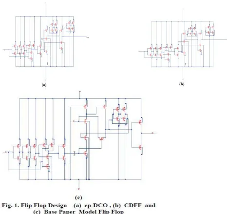
In this paper I have took some flip flop which exist already these designs are done in 130n meter technology and compare with other design which are done by changing the pulse generator fig 1(a) shows a classic explicit pulse triggered flip flop . In this design pulse generator is designed in a such way that four inveters are taken along with a Nand gate and a tspc latch.This design face a problem of switching
been proposed [3],[4],[5],[6],[7] to over come the problem of above design in the CDFf an extra transistor of nmos is taken and given to the Q-fdbk which controls the discharge and make the input data remains constant but this design face a problem of worst delay so to overcome this problem another pulse triggered flip flop is designed .First a weak pmos transistor is taken and gate of pmos transistor is is connected to the ground and second a nmos pass transistor is used which controlled by the pulse clock is included so that input data can drive node. The node level can thus be quickly pulled up to shorten the data transition delay [8]
II. PROPOSEDMODEL
A novel explicit pulse triggered flip flop is designed. This flip flop consist of a pulse generator and a transmission gate .this new explicit pulse triggered flip flop works on three stages i.e. pulse generator, latch and a bistable element. used .They are implicit and explicit type pulse triggered flip flops. In implicit type of pulse triggered flip flop the pulse generator is present inside the flip flop where as in the explicit pulse triggered flip flop the pulse
generator is present outside the flip flop [1], [2]
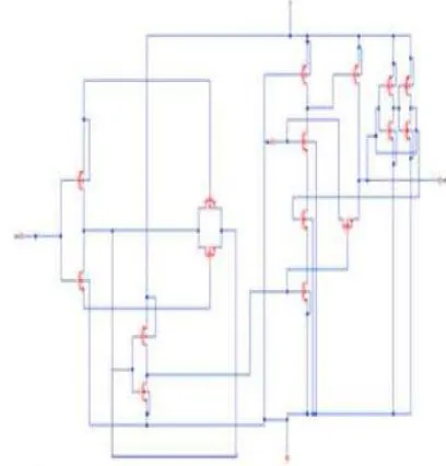
Fig.2. Schematic Of The New Flip Flop Design Fig 2 Shows A Latch Which Consider With A Nmos Pass Transistor And Weak Pmos Transistor To Over Come The Problem Of Fliping Of The Output.
Principle Working: -
Stage1: When Clock Is Given As Input To The First Cmos Inverter And Its Output Is Given As A Input To The Transmission Gate And The Out Of It Is Given As The Input Of The Second Cmos Inverter And Its Output Is The Pulse Generator Output his pulse generator generates the pulse and it is given to the latch.
Stage2: when the pulse generator gives 1 as input to the latch .since the latch consists of pmos and nmos transistors and when it is given „1‟ then all pmos transistors are in off state i.e. non conducting and the nmos transistors are in on state so it passes the data which applied to it .since the data input is signally feed through to the pass transistor.
is also called regenerator property. When clock is „0‟ then all the nmos transistors are in off state and pmos transistors are in on state .these transistor retrieve whatever data present in bistable element as a output.
III. APPLICATION
By using a explicit pulse triggered flip flop a Synchronous counter with 3 bits is designed as shown in fig 3.which can be expanded to 4,8,12 and 16 bit.
IV. SIMULATION RESULTS
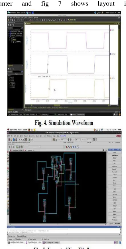
The proposed pulse triggered flip fliop is designed against existing flipflop design and this design is designed in GENERIC 130n meter technology and simulated both in pre-layout and post-layout simulation . after simulation delay ,number of tansistor and power is less compare to existing flip flop this is shown in table1 and fig 4 shows waveform of new explicit pulse triggered flip flop and fig 5 shows layout of it. And fig 6
counter and fig 7 shows layout it
Fig. 7. Layout of a 3-Bit Synchronous Counter of Proposed Flip Flop
V. CONCLUSION
REFERANCES
[1] Xia W.Q.shui,X.Y and Yao, W.L “Dual-vth based double-edge explicit-pulseed level-converting flip-flop” in IEEE-International Conference on Electronics ,communications and control (ICECC),(2011)
[2] Bhargavaram,D.and Pillai,M.,”low power dual edge triggered flipflop”. in Advance in Engineering,science and Management (ICAESM),International Conference on IEEE,(2012),63-67.
[3] B. Kong, S. Kim, and Y. Jun, “Conditional-capture flip-flop for
statistical power reduction,” IEEE J. Solid-State Circuits, vol. 36, no. 8, pp. 1263–1271, Aug. 2001.
[4] N. Nedovic, M. Aleksic, and V. G. Oklobdzija, “Conditional pre charge techniques for power-efficient dual-edge clocking,” in Proc. Int. Symp. Low-Power Electron. Design, Aug. 2002, pp. 56–59.
[5] P. Zhao, T. Darwish, and M. Bayoumi, High-performance and low power conditional discharge flip-flop,” IEEE Trans. Very Large Scale Integr. (VLSI) Syst., vol. 12, no. 5, pp. 477–484, May 2004.
Author’s Profile:
K.LAVANYA, completed her graduation in SBIT in The year 2013 and pursuing her m. tech in SaharaCollege of Engineering for WomenWarangal, India.