Implementation of Parallel Self Timed Adder
Using Modified GDI Logic
V.Preethi
1, N.Subbulakshmi
2Student, Department of ECE (PG), Sri Ramakrishna Engineering College, Coimbatore, India1 Assistant Professor, Department of ECE, Sri Ramakrishna Engineering College, Coimbatore, India2
ABSTRACT:This paper presents comparisons of logic style based on different logic functions in which Modified Gate Diffusion Input logic (Mod-GDI) is power-efficient than Gate Diffusion Input logic (GDI) and Complementary Metal Oxide Semiconductor CMOS logic design. When CMOS logic is used number of transistors increases and hence area increases. By using GDI logic area and power dissipation decreases but it suffers from the problem of bulk connections and high swing degradation. Mod-GDI is used to reduce the swing degradation problem which consists of only two transistors, by changing its input configuration number of boolean function are obtained. The practical circuit arrangements reveal Mod-GDI to be more superior to GDI and CMOS logic with respect to speed, area, power dissipation and power. Simulation results shows up to 50% reduction in area and power dissipation in Mod-GDI. This logic is used for designing fast, low power circuits with reduced number of transistor as compared to CMOS techniques, while improving power characteristics.
KEYWORDS: Asynchronous logic, CMOS logic, GDI logic, Modified GDI logic
.
I. INTRODUCTION
II. NEEDFORASYNCHRONOUSCIRCUIT
Most digital circuits designed and fabricated today are synchronous. In essence, they are based on two fundamental assumptions that greatly simplify their design[2]. They are all signals are binary, and all components share a common and discrete notion of time, as defined by a clock signal distributed throughout the circuit. Asynchronous circuits are fundamentally different; they also assume binary signals, but there is no common and discrete time. Instead the circuits use handshaking between their components in order to perform the necessary synchronization, communication, and sequencing of operations. Expressed in synchronous terms which results in a behaviour that is similar to systematic fine-grain clock gating and local clocks that are not in phase and whose period is determined by actual circuit delays – registers are only clocked where and when needed. This difference gives asynchronous circuits inherent properties that can be exploited to advantage in the areas are low power consumption due to fine-grain clock gating and zero standby power consumption, high operating speed which is determined by actual local latencies rather than global worst-case latency, robustness towards variations in supply voltage, temperature, and fabrication process parameters, better composability and modularity because of the simple handshake interfaces and the local timing, no clock distribution and clock skew problems, since there is no global signal that needs to be distributed with minimal phase skew across the circuit. When synchronous circuits are used there is problem of global clock distribution and clock skew and hence to avoid this problem asynchronous circuits are used.
III. PASTA
Parallel single-rail self-timed adder is based on a recursive formulation for performing multibit binary addition. The operation is parallel for those bits that do not need any carry chain propagation. Thus, the design attains logarithmic performance over random operand conditions without any special speedup circuitry or look-ahead schema. A practical implementation is provided along with a completion detection unit. The implementation is regular and does not have any practical limitations of high fanouts. A high fan-in gate is required though but this is unavoidable for asynchronous logic and is managed by connecting the transistors in parallel. The adder first accepts two input operands to perform half additions for each bit. The general architecture of the adder is shown in Fig.1. The selection input for two-input multiplexers corresponds to the Req handshake signal and will be a single 0 to 1 transition denoted by SEL. It will initially select the actual operands during SEL = 0 and will switch to feedback/carry paths for subsequent iterations using SEL = 1. The feedback path from the HAs enables the multiple iterations to continue until the completion when all carry signals will assume zero values.
A. MODIFIED AND GATE
When input G = A, N = B, P = 0, SP = VDD [1 or High], and SN = 0, then output D = A.B which is AND function. Fig.2 shows input configuration for Mod-GDI AND Function, where; at Node „1‟ input G = A is given, at Node „2‟ input N = B is given, at Node „3‟output D = A.B is taken, at Node „4‟ input P = 0 is given.
Fig.2 Schematic for Modified GDI AND gate Fig.3 Simulation for Modified GDI AND gate
B. MODIFIED XOR GATE
When input G = B, N = ABAR, P = A, SP = VDD [1 or High], and SN = 0, which is a XOR function. Fig 4 shows input configuration for Mod-GDI XOR Function.
Fig.4 Schematic for Modified GDI XOR gate Fig.5 Simulation for Modified GDI XOR gate
C. MODIFIED MULTIPLEXER
Fig.6 Schematic for Modified GDI Multiplexer Fig.7 Simulation for Modified GDI Multiplexer
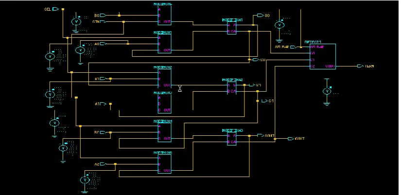
IV.PASTAUSINGMODIFIEDGDI
Parallel self Timed Adder is designed for three bit using Modified GDI logic. When the adder is designed using this logic 29 transistors are required. For the design of same adder using CMOS and GDI logic only 129 and 45 transistors are required and the results are tabulated.
Fig.8 Schematic for PASTA using Modified GDI logic
TABLE I
PARAMETERS CMOS LOGIC GDI LOGIC MODIFIED GDI
LOGIC
AREA 129 transistors 35 transistors 29 transistors
POWER DISSIPATION
V. SIMULATION RESULT
Fig.9 Simulation for PASTA using MODIFIED GDI logic
VI. LAYOUT
Design Rule Check (DRC) is the area of Electronic Design Automation that determines whether the physical layout of a particular chip layout satisfies a series of recommended parameters called Design Rules. Design rule checking is a major step during Physical verification signoff on the design, which also involves LVS (Layout versus schematic)
Check. The Layout Versus Schematic (LVS) is the class of electronic design automation (EDA) verification software that determines whether a particular integrated circuit layout corresponds to the original schematic or circuit diagram of the design. LVS check recognizes the drawn shapes of the layout that represent the electrical components of the circuit, as well as the connections between them.
Fig.11 Layout for Modified GDI XOR gate
Fig.12 Layout for Modified GDI Half Adder Fig.13 Layout for PASTA using Modified GDI
VII. CONCLUSION
CMOS logic, GDI logic and Modified GDI logic for Parallel asynchronous self-timed adder is presented. Hence, Modified GDI logic provides full swing and also solves the problem of bulk connections. Thus, Modified GDI logic provides low power and less area when compared with CMOS and GDI logic.
REFERENCES
[1] D. Geer, “Is It Time For Clockless Chips? [Asynchronous processor chips],” IEEE Comput., vol. 38, no. 3, pp. 18–19, Mar. 2005. [2] J. Sparsø and S. Furber, Principles of Asynchronous Circuit Design. Boston, MA, USA: Kluwer Academic, 2001.
[3] P. Choudhury, S. Sahoo, and M. Chakraborty, “Implementation of Basic Arithmetic Operations Using Cellular Automaton,” in Proc. ICIT, 2008, pp. 79–80. [4] M. Z. Rahman and L. Kleeman, “A delay matched approach for the design of asynchronous sequential circuits,” Dept. Comput. Syst.Technol., Univ. Malaya, Kuala Lumpur, Malaysia, Tech. Rep. 05042013, 2013.
[5] Gary Yeap, “ Practical Low Power Digital VLSI Design”, Kluwer Academic Publishers.
[6] N.H.E.Weste, David Harris Ayan Banerjee, “CMOS VLSI design, Pearson Education Publication, Sixth Impression, 2008.
[7] Arkadiy Morgenshtein, Alexander Fish & Israel A Waganer, “Gate Diffusion Input ( GDI): A power efficient method for Digital Combinational circuits”, IEEE Transactions on VLSI Systems, Vol 10, No.5, Oct 2002.