Abstract:
Guled, Mohamed Ibrahim, Optical Network Processor Design For Just-In-Time
Signaling Protocol Message Engine Design. (Under the directions of Paul D.
Franzon)
Optical Network Processor Design
For
Just-In-Time Signaling Protocol Message Engine Design
by
Mohamed Guled
A thesis submitted to the Graduate Faculty
of
North Carolina State University
In partial fulfillment of the requirement for the Degree in
Master of Science in Electrical Engineering
Department of Electrical and Computer Engineering
Raleigh
2002
Approved by:
_____________________
Dr. Paul D Franzon
Chairman, Advisory Committee
_________________ ___________________
Biography
Mohamed Guled was born in Mogadishu, Somalia in the year 1975. He attended his
Undergraduate studies in St. Petersburg State Technical University pursuing the
Acknowledgements
There is never a job in the world that can single handedly be done. This work is no
exception. Let me begin by naming my advisor, Dr. Paul Franzon, who was always
available for any doubt or question, howsoever elementary or trivial they might be.
Without his insight and guidance, needless to say, this project would be have never got
completed. Also, many thanks to my committee members, Dr. Brian Hughes and Dr.
Keith Townsend, for their valuable input, encouragement and for reviewing my thesis.
This project was a joint effort between NCSU and MCNC, RTP and I would like to
especially thank Dan Stevenson, Director of Advanced Networking Research group at
MCNC for all the support during the course of the project. I also thank everyone who was
part of the team for the Jumpstart Project at NCSU and MCNC for the endless
discussions that we had.
Special thanks to Monther Aldwairi, who worked with me in this project for the last one
and half years. His dedications and continuous contribution of the project played major
role implemented this project and actually getting it to work. Your sincerity and hard
work were source of inspiration to me. Thank you for your late nights and for tolerance
me.
Thanks also to Mike Pratt and Mark Cassada over at MCNC who had major impact
specifying, designing, documenting and implementing the project in their part of the
project. Needless to say, they deserve accolades as much as I do.
Thanks to Patrick Hamilton and Basil Haddad who at later stage of project contributed
there time and energy testing major components of the design.
Table of Contents
List of Tables……….vii
List of Figures………..viii
1 Introduction………...1
1.1 Motivation and Contributions………1
1.2 Thesis Organizations………..………3
2 Architectural Overview……….4
2.1 System Level Analysis..……….4
2.2 Register Access Block Interface to Message Engine……….6
3 Signaling Definition…...……….7
3.1 Overview……...……….7
3.2 Basic Assumptions about Signaling..……….7
3.3 Cross-Connect Configuration for Connection Setup……….8
3.4 Scheduler Complexity……….……….10
3.5 Burst Delay………...……….11
3.6 Connection Phases………...12
3.7 Message Types…..………...12
3.6 Signaling Message Format………...13
4 Design Flow of The Message engine………..16
4.1 Architectural Overview of The Message engine……….16
4.2 Register Access Block Module………17
4.3 Ingress Message Engine Interface Module………..23
4.4 Message Parser Module………...24
4.5 CRC Checker/Generator………..25
4.6 Forwarding Engine………..26
4.6.1 Message Engine Addressing Scheme………...26
4.6.2 Forwarding Engine Configuration………....29
4.6.3 Forwarding Engine Operation………..30
4.7 State Connection Maintenance Module………...32
4.7.1 Mirror Cross-Connection Table………33
4.8 Field Update Module………...40
4.9 ACK/NACK Generation Module………41
4.10 Output Port Requester Module………..41
4.11 Message Reassembly Module………42
4.12 Crossbar Module………43
4.12.1 Control Bus……….44
4.12.1.1 Synchronous Bus Arbiter……….44
4.12.2 Data Bus………..45
4.13. Egress Message Engine Interface Module………47
4.14 Pipelining In The Design………...48
4.15 Message Engine Scalability Issues………51
4.15.1 Crossbar Scalability………51
4.15.2 Space Division Architecture………...53
4.15.3 Shared Memory Architecture………..54
5 Test Plan………..55
5.1 Introduction………..55
5.2 Test Goals………55
5.3 Test environment.………56
5.3.1 Test Environment For The Simulation System………56
5.3.2 The Hardware Test Environment……….56
5.3.3 ATDnet (Government laboratory in Washington DC area)……….57
5.4 Test Suites………58
6 Conclusions and Future Work………59
Reference:……….61
List of Tables
Table 1: Message Engine Message Types………12
Table 2: Signaling Message definition…..………14
Table 3: Hardware Switched Message Type ………15
Table 4: RAB Storage Elements…………... ………18
Table 5: Egress Message Ready Interrupts... ………20
Table 6: Hardware Failure Condition Interrupts.………...…………20
Table 7: Other Interrupts………... ………21
Table 8: IME Configuration Signals………. ………22
Table 9: Forwarding Table Format..………. ………29
Table 10: Forwarding Table Architecture…..………32
Table 11: Mirror Cross Connection Table...………33
Table 12: Mirror Cross Connect Interface Table (Setup and Release).……….35
Table 13: Mirror Cross Connect Interface Table (Connection Timeout).……….37
List of Figures
Figure 1: System Block Diagram……….4
Figure 2: Board Level Data Flow...……….5
Figure 3: Processor to FPGA Interconnect……….……….5
Figure 4: Ingress And Egress ME Block Diagrams……….6
Figure 5: ME Interface With RAB………...7
Figure 6: Signaling Message Structure………..13
Figure 7: Top Level Block Diagram of The ME..……….17
Figure 8: RAB Interface With ME..………...22
Figure 9: IME Logic Diagram…....………...24
Figure 10: Message Parser Logic Diagram………..……….…25
Figure 11: CRC Checker/Generator………..……….…………26
Figure 12: Proposed Addressing Scheme. ………..……….….27
Figure 13: Domain Hierarchy……….………..……….…27
Figure 14: FE Logic Diagram………..……….……….30
Figure 15: Functional and Block Diagram of The SCM………..……….….39
Figure 16: Filed Update Block Diagram………..……….….40
Figure 17: Crossbar………..……….….43
Figure 18: Control-Bus Logic Diagram.………..……….….44
Figure 19: Synchronous Bus Arbiter………..……….…..45
Figure 20: Arbiter Element Logic Diagram.………..……….…...46
Figure 21: Data Bus Logic Diagram...………...………..……….….47
Figure 22: EME Interface Module...………...………..……….….48
Figure 23: Effects of T_fwd...………...………..……….…………..52
Figure 24: Trade-off Number of ports vs. Time of processing Each Message…….….…53
Figure 25: Banyan Networks...………...………..……….…………54
Figure 26: Shared Memory Architecture………...………..……….….55
Chapter 1
Introduction
1.1 Motivation and Contributions
Light can be sent long distances through high quality fiber with little dispersion or attenuation. The 1.5um
wavelength that is commonly used in communication systems corresponds to a frequency of 2*1014Hz. A
bandwidth of even 0.1% of this carrier, 100GHz,is wider than any encountered in electrical systems.
Optical systems are also much less susceptible to interference in comparison to electrical systems. A
combination of the above factors has made optical communications the method of choice for distances over
100m, thus, requiring the development of network processor design for optical burst switching networks.
With the proliferation of the Internet and the exponential growth in bandwidth demand, Wavelength
Division Multiplexed (WDM) all optical transmission systems are fast becoming an attractive choice for
future telecommunication applications. The WDM approach is to keep the bit rate the same and add more
wavelengths, each carrying data at this bit rate. WDM is the most practical option today in comparison to
the Space Division Multiplexing (SDM) and the Time Division Multiplexing (TDM) approaches. The SDM
approach requires more fibers and a separate set of optical amplifiers for each fiber, which in turn
contributes to a significant expense over long distances. Optical modules of very high frequency are
needed in TDM to obtain speed increase in individual channels. The distance limit due to chromatic
dispersion and Polarization mode dispersion is much larger for WDM transmission systems than for
equivalent TDM systems due to lower bit rates per channel employed in the WDM approach. WDM
systems are also more modular and cost effective compared to TDM in designing more complicated
signaling message protocol (Just-In Time Protocol Accelerator Card) and associated architecture for WDM
burst-switching network. The premise of this architecture is simple – data, aggregated in bursts can be
transferred from one end point to the other by setting up light path just ahead of the data to set up the path.
Upon completion of data transfer the connection is timed out. The basic architectural assumptions are:
signaling is done out of band, data is transparent to the intermediate network entities, i.e. no electro-optical
conversion is done in the intermediate nodes, most of the intelligence of the network is concentrated on the
edge and global time synchronization between nodes is assumed.
Basic switch architecture presumes having a number of input and output ports, each carrying multiple
wavelengths (~160 in the prototype model). A separate wavelength on each port is dedicated to carrying the
signaling traffic. Any wavelength on an incoming port can be switched to either the same wavelength on
any outgoing port (no wavelength conversion), or any wavelength on any outgoing port (partial or total
wavelength conversion).
In this architecture, a signaling message attempting to setup a path for burst to travel from one point to the
other must inform all intermediate switches of the arrival of the burst to allow them to set up their mirror
cross-connection configuration to channel the data on one of the data wavelengths.
The basic network architecture is presented in the figure below. Some of its important components are
explained in further chapters. The figure should be used as reference architecture.
c
hannel fiber
)
OBSE
OBSE
s
ignaling channel
1.2 Thesis Organization
Chapter 2 starts off with architectural analysis of the message engine and its interface to the rest of the
system. Message engine hardware processes incoming Just-In-Time protocol signaling messages that are
sent on an optical fiber’s control signaling channel. The ME makes wavelength reservations requests to the
hardware controller of an optical switch matrix, and appropriate Just-In-Time protocol messages are output
by the Message engine (ME) on the control-signaling channel.
Chapter 3 discusses the signaling definition of the message engine that only addresses one aspect of the
network management and that is the connection setup. Depending the type of the connection being setup,
the signaling protocol performs sever functions: connection declaration, setup the connection route, data
transmission, maintain the state of existing connections and tear down the route of the connection.
Chapter 4 highlights the design flow and discusses in detail the message engine components. Justification is
provided for the choice of the individual modules and how they are pipelined in the design. The chapter
concludes with a brief discussion of scalability issues.
Chapter 5 describes the test goals, the test environments built for the computer simulation, testing
methodology and test suite development. There is couple of test goals that were carried out. The first set of
the test scripts tested the valid message formats and sequences for various services our protocol was
intended to support and used to validate normal operation of the signaling protocol implementation in all
three test environments. The second test script exhaustively tested abnormal message formats and
sequences and was used to validate the correct operation of the hardware implementation.
Chapter 6 summarizes the conclusions drawn on the basis of the results obtained. Suggestions for future
Chapter 2: Architectural Overview
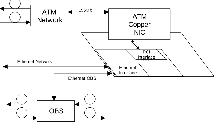
2.1 System Block Diagram
ATM
Copper
NIC
155Mb
Ethernet OBS
OBS
ATM
Network
Ethernet Interface
8250 PCI Interface Ethernet Net work
Figure 1: System Block Diagram
The JITPAC (Just In Time Protocol Acceleration Card) is standalone development card. It supports a
Single PCI port and two 100/10 Ethernet ports. An ATM copper NIC interfaces the PCI port. The
Signaling messages is transported over the ATM link to the JITPAC card. The JITPAC card contains
A local Motorola processor MPC8260 with external bridge device and Message Engine implemented as an
Altera 20K400C FPGA. The local processor will control all external ports (PCI, Ethernet Network,
Ethernet OBS). The PCI port Control and data interface is directly connected to the MPC8260 processor.
The Hardware Message Engine receives signaling data packets from the local processor via the 603e
(64-bit) bus. Figure 2 shows the board level data flow of the between the ATM signaling layer and the
JITPAC. Figure 3 shows Motorola processor MPC8260 and the Message Engine implemented as
Figure 4 shows the Ingress and Egress Message Engine block diagram.
JITPAC
Processor FPGA 603e Bus 33Mhz 64bit wide bus R A B IE Processor Port /λ6 0 3 P C I ATM Card
PCI Int f 33Mhz 32bit wide bus
Figure 2: Board Level Data flow
GPIO IRQ
FPGA Config Control
MPC8260
APEX 20K
R A B 603 Data Bus
603 Address Bus
Bus Control
Interrupts
Message Engine Status ADDR [31:0] DATA [63:0] CS/PWE/etc. GPIO Clk Future Interface Connectors LED Bank[8] Debug header[32] JTAG
JTAG/ Programmer Port
FPGA
EP20K400C
Cont rol Signals
Clk
603 data bus
Interrupt Port Active bits 603 Addr bus
LED Bank[8]
Debug header[ 32]
FPGA Parallel Configuration
Port
Future Interface Connectors
RAB
IME0 IME1 IME2 IME3
EME0 EME1 EME2 EME3
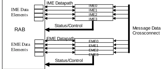
Figure 4: Ingress and Egress Message Engines Block Diagrams
2.2 Register Access Block (RAB) Interface To Message Engine
The RAB is a module in the FPGA, which provides a method of communication between the JIT software
Running on the MPC8260 microprocessor and the Message Engines (MEs) in the FPGA. All RAB storage
Elements are memory-mapped and accessible via the 603 bus. In addition, there are four-message engine
Status signals, five interrupt request signals, and several control signals used for FPGA configuration. The
Viewed as a single bank of SRAM, 32-bits wide. Software has read access to all storage locations in the
RAB except the Ingress Message FIFOs and Forwarding Tables. From the perspective of the MEs, the
RAB consists of a large array of registers, some of which are inputs to ME modules and some of which are
Outputs from the MEs. The figure 5 below shows the interface signals between RAB and Message Engine.
Status/Control IME Data
Elements
EME Data Elements
Status/Control IME0 IME1 IME2 IME3
EME0 EME1 EME2 EME3 IME Datapath
EME Datapath
RAB Message Data
Crossconnect
Figure 5: Message Engine Interface with RAB
Chapter 3: Signaling Definition
3.1 Overview
The signaling definition of the message engine that only addresses one aspect of the network management
and that is the connection setup. Depending the type of the connection being setup, the signaling protocol
performs sever functions: connection declaration, setup the connection route, data transmission, maintain
the state of existing connections and tear down the route of the connection. These phases can be
accomplished by signaling protocols in different fashion, depending on the assumptions made about the
network: the reliability of the individual links, scheduling capabilities of the switches and other factors.
3.2 Basic Assumptions About Signaling
Its assumed the following about the functionality of the signaling channels:
• Signaling is done out of band
• Signaling channel is presumed to posses low bit error rate (10^-15+)
The second bullet requires an explanation: making the signaling protocol reliable link by link requires
either positive or negative acknowledgements and the ability to retransmit lost messages. In Just-In-Time
environment, where burst travels with short delay behind signaling message, retransmitting a lost message
may delay it enough to render it useless (the burst may arrive at the switch before the signaling message
that sets up its path). Adding to this the increased burden on the signaling engine by making the signaling
protocol reliable, we came to a conclusion that this feature is in fact not desirable in a JIT optical burst
switch network.
3.3 Cross-Connect Configuration for Connection Setup
In literature on JIT OBS networks, four ways have been identified of configuring the switch fabric of an
incoming connection:
1. Explicit setup and tear down: signaling messages sent by the source trigger the intermediate
switches on the path to configure the cross-connect for the incoming connection and then to
restore the original configuration.
2. Explicit setup with estimated teardown: signaling message sent by the source indicates to the
intermediate switches when the cross-connect needs to be configured and the same message
carries the information about the estimated duration of the burst, so the switch knows when the
burst has passed and can allow the same cross-connect element to be used for a different
connection.
3. Estimated setup and explicit teardown: signaling message carries information about the estimated
start of the burst, so the switch can delay configuring the cross-connect based on that estimate,
however there is an explicit teardown done by special signaling message, telling the switch the
connection is finished.
4. Estimated setup and teardown: single signaling message carries enough information about the
burst to allow the intermediate switch to estimate both the start and the end of the burst to allow
the intermediate switch to estimate both the start and the end of the burst so that it configures the
The difference in these schemes is in the number of signaling message needed to setup a connection and in
the complexity of the scheduler needed to maintain the state of the intermediate switch.
The first scheme requires the simplest scheduler. In it the scheduler only needs to maintain the information
about the current occupancy of its cross-connect elements and this information is explicitly manipulated by
the arrival of special signaling messages. Its disadvantage lies in the amount of the signaling traffic
required for short bursts (two messages each) and in the amount of time the cross-connect is configured
compared to the time it is actually utilized by the connections.
Schemes (2) and (4) only require one signaling message per connection, however they require an
increasingly more sophisticated schedulers to be able to schedule connections passing through the switch.
Scheme (3), like scheme (1), requires two signaling messages.
Scheme (2) requires a scheduler to maintain an estimated deadline, when the specific cross-connect element
will no longer be utilized by the connection, so it can use it for new connections. Scheme (3) and (4)
require the scheduler to maintain a limited temporal horizon per outgoing channel (perhaps implemented as
sliding window) so the scheduler can tell whether at given moment in the future a channel will be occupied
or not. These schemes, however, become increasingly more efficient in the use of the network bandwidth,
in that they require that cross-connect is configured for less and less time compared to the time it is actually
utilized by the connection, thus resulting in lower blocking probability.
In our approach to signaling we decided to limit the definition to schemes (1). Scheme (3) is not very
useful, since it has both the disadvantage of requiring more signaling traffic and a more complex scheduler.
Scheme (4) use is limited due to the complexities of the scheduler.
The first signaling scheme we called it “Explicit Teardown”, while the second one we called it “Timed
Teardown”. One further aspect of signaling to be discussed is the state maintenance of long-lived
time, scheme (2) requires that and since rarely a user can specify that a connection will be required for a
precise duration of time, scheme (2) requires what we call “Keep-alive” messages, which are sent by the
originator of the connection and prevent the intermediate nodes from otherwise timing out the state of the
connection.
Additionally, these keep “Keep-alive” messages are also desirable for scheme (1) for the following reason
– in our early assumptions was stated that signaling channel is considered unreliable, therefore the explicit
teardown messages maybe lost, thus leaving certain connections permanently open. To avoid that a
maximum time-to-live is required for an established connection with a periodic “Keep-alive” to refresh its
state.
Based on the above discussion, “Keep-alive” messages will be used to maintain the state of long-lived
connections in both schemes (1) and (2).
Finally, as was mentioned in the architectural assumptions, two traffic types are defined: bursts and circuit
emulation. A burst may last a short time and require no state maintenance, or it can last long time so that
state maintenance with “keep-alive” messages is needed, thus becoming a light-path. Circuit emulation is
similar to such a light-path in its duration and maintenance mechanism, however it does not utilize a
wavelength for 100% of the time, but rather for known durations of time with known period.
3.4 Scheduler Complexity
The above section has mentioned scheduler complexity in relation to the type of the signaling flow utilized.
The “Explicit Teardown” scheme has the lowest required scheduler complexity – a simple occupied
indication for each cross-connect element used for a specific connection (output channel for non-blocking
switch architectures). Next is complexity is the “Timed Teardown”, which requires that a single deadline is
kept per switching element in a connection, to tell the scheduler when it can use this element for another
connection (a simple comparison of the deadline with the switch local time is required to determine
Both schemes (3) and (4) estimate the beginning of the burst, which by itself requires keeping a limited
knowledge of the future state of the switching element (unlike the first two schemes, which only require
knowledge of the present state). This in itself means that amount of information per switching element is
increased from a single number to an array; whose size depends how far into the future the switch is willing
to schedule. In addition to the space complexity, there arises a processing complexity in the scheduler,
which now has to decide whether it can fit a certain connection into schedule before the next one arrives.
Thus schemes (3) and (4) require a relatively complex scheduler mechanism. If circuit emulation (well
defined periodic bursts) is added to the supported connection types, the scheduler becomes even more
complex, because with circuit emulation, unlike the single burst traffic type, several connections can be
utilizing the switching element at the same time (their busy periods cannot overlap, of course). Thus a
scheduler that can support circuit simulation must by necessity be even more complex than the one needed
to support schemes (3) and (4). Hence, Circuit emulation traffic type was not used in the initial
implementations of this protocol.
3.5 Burst Delay
As was stated in the architecture section, the transfer of data across the network is achieved by sending a
signaling message ahead of the actual burst in order to set up the path for it. The idea is that while the
signaling message traverses the network, it needs to stay ahead of the burst in order to give intermediate
switches time to configure their cross-connect mirrors. The delay between the burst, which is optically
transparent to the network, the signaling message experiences processing delay at every intermediate
switch. Thus the problem becomes that of estimating the initial burst delay ahead of time before the
message is sent. This estimate is tied to the number of hops on the connection path. While the exact
mechanism to perform and refine this estimation remains the topic of further investigation, its important to
understand that this estimation mechanism must be present in the network in order for it to function. In our
3.6 Connection Phases
Each connection in out Optical Burst Switched (OBS) network goes through a number of well-defined
phases:
a) Session Declaration
b) Connection Route Setup
c) Data Transmission
d) State Maintenance
e) Session Release
Its worth noting that these are uni-cast connections and in relation to signaling schemes earlier also have all
of these phases, however some of them are collapsed into single step. For example the Setup message
serves to: Announce the connection to the network (Session Declaration), setup the route of the connection
(Connection Route Setup) and announce the arrival of the burst (Data Transmission). Thus, combining the
first three phases, which are followed by either explicit or implicit session release. These connections have
state maintenance phase. This phase is intended for long-lived connections that require the “Keep-Alive”
message as described above.
3.7 Message Types
Basic message types required to setup a uni-cast connection in JIT OBS network are described in the table
1 below:
Table 1: Message engine message types
Message Type Message Function Currently Supported
Session Declaration Notify the network that a persistent – route
connection is being setup.
No
Setup Notify the network that a burst is arriving. Yes
Keep-Alive State maintenance message periodically sent by
the source.
Yes
Release In explicit release scheme tells the intermediate
node the connection is being torn down.
Failure Indicates general failure of connection setup Yes
Connect Optionally returned by the destination client
node to the source to acknowledge the
connection setup.
Yes
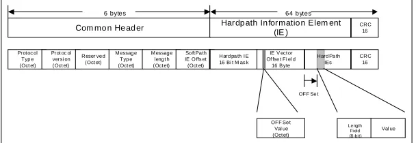
3.8 Signaling Message Format
Just-In-Time protocol will utilize a single signaling message structure. Its separated into three parts:
common header, hard-path information elements and soft-path information elements. The concept of an
information element is borrowed from ATM. Each information element carries data that pertains to a
particular aspect of the signaling protocol in which it is being utilized.
The information elements are separated into hard-path and soft-path, depending on whether they are intended to be
processes by hardware or software, respectively. The structure of information elements in both hard-path and
soft-path is the same – it’s a TLV triple (type, length, value). This uniformity allows migrating information elements
from soft-path to hard-path as hardware matured so that it is capable of processing more information elements.
Figure 6 below shows the signaling message structure.
Com mo n He ad er Hardp ath In formatio n Elem ent (IE )
Prot oc ol Typ e (Oct et)
Prot oc ol versi on (Oct et) M essage Typ e (Oct et) M essage lengt h (Oct et)
So ft Path IE O ffs et (Oct et)
Hard pa th I E 16 Bi t M as k
IE V ect or Of fse t Fi el d
16 B yte
OFF Set Val ue (Oct et) Length Fi eld (8-bit) Val ue OFF Se t
6 bytes 64 bytes
CRC 16
CRC 16 Hard Pa th
IEs Reser ved
(Oct et)
Figure 6: Signaling message structure
Inside the hard-path and soft-path headers there is information about the number of information elements
presents in each header. Each header has a variable length vector of offsets for each information element
The hard-path header makes it easier to determine which particular IEs are present in the header by
providing a bit-vector. A single bit set in vector in a specific position corresponds to specific IE type
present in the header. This makes it easy for the hardware to parse the header and determine invalid IE
combinations. Of course, the number of hard-path IEs in the header is limited to the length of the bit-vector.
Unlike the hard-path header, which allows the parser to see which particular IEs are present in it, the
soft-path header simply presents a vector of <type, offset> for each IE. Thus the software scans the entire vector
before it knows all the IEs present in the soft-path header. However, unlike the hard-path header, the
number of IEs that can be present in the soft-path header is unlimited.
The common header that is present in each signaling message has the information about the specific
signaling protocol this message relates to (connection setup, routing etc.), protocol version used to create
the message, message type and over all length and the offset to the beginning of the soft-path header. This
last offset allows the software and hardware to begin parsing their respective headers in parallel, without
software having to parse the hard-path first.
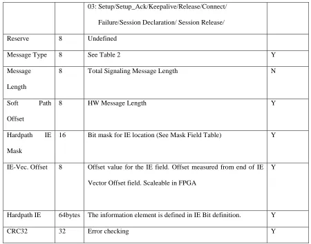
Finally, each message is appended with a CRC-32 sequence for integrity verification. The table 2 below
shows the signaling message definition. Figure 3 table shows Hardware message switched types.
Table 2: Signaling message definition
Message
Partitions
Bits
(Max)
Description Hardware
Supported
Protocal Type 8 Undefined N
Protocol
Version
8 Version Defines Hardpath IE and Softpath IE
00: Proto/Undefined
01: Setup/Setup_Ack/Keepalive/Release
02: Setup/Setup_Ack/Keepalive/Release/Connect/
Failure
03: Setup/Setup_Ack/Keepalive/Release/Connect/
Failure/Session Declaration/ Session Release/
Reserve 8 Undefined
Message Type 8 See Table 2 Y
Message
Length
8 Total Signaling Message Length N
Soft Path
Offset
8 HW Message Length Y
Hardpath IE
Mask
16 Bit mask for IE location (See Mask Field Table) Y
IE-Vec. Offset 8 Offset value for the IE field. Offset measured from end of IE
Vector Offset field. Scaleable in FPGA
Y
Hardpath IE 64bytes The information element is defined in IE Bit definition. Y
CRC32 32 Error checking Y
Table 3: Hardware switched message types
Message Type Value Definition
Session
Declaration
00 Notify the network that a persistent-path Unicast or Multicast connection is
being set up. This is a session declaration that set a path for continuous data
path allocation?
Setup 01 Notify the network that a burst is arriving. This type session is for single burst
of data and will be followed eventually with a release.
Declaration
ACK
02 Acknowledgement of Session Declaration by the called party (Client Node or
Setup ACK 03 Acknowledgement from the first Ingress switch to the Client Node.
Failure 04 General connection failures
Connect 05 Message returned to the Calling switch from the Called switch
Keepalive 06 Message sent to maintain connectivity on a route due to that channel
utilization. The keep alive signal prevents a timeout condition from occurring.
Release 07 Releases an existing unicast connection (explicit teardown) or used to
teardown session routing tree in a multicast connection. Also used to force a
teardown due to lack of resources
Session
Release
08 Used to terminate a session
Add Party 09 Adds new party to existing to existing multicast session
Add Party
ACK
0A Acknowledges receipt of the Add Party message
Drop Party 0B Drops party from a multicast session
Drop-Party
ACK
0C Acknowledges that the Party was dropped
Chapter 4 Design Flow of The Message Engine
4.1 Architectural Overview of The Message Engine
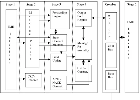
The message engine consists of 13 modules that are pipelined in 5 different stages. The first phases of the
JIT protocol, its assumed that the message engine process one message at a time. Messages are loaded by
software running on the MPC8260 microprocessor. The figure below 7 shows the block diagram and the 5
different stages of how message is being processed inside the message engine.
Figure 7: Top level block diagram of the Message Engine
4.2 Register Access Block (RAB) Module
The Register Access Block (RAB) is a module in the FPGA, which provides a method of communication
between the JIT software running on the MPC8260 microprocessor and the Message Engines (MEs) in the
FPGA (See figure 3). It consists of a large storage array with interface modules to the 603-bus and the
Message Engines. The table 4 below lists some of the information that is stored in the RAB. Read/Write
(RW) permissions are also listed for the processor and the Message Engines.
Table 4: RAB Storage Elements
Read/Write Data Type
8260 ME’s
Stage 1 Stage 2 Stage 3 Stage 4
IME I n t e r f a c e M e s s s g e P a r s e r Forwarding Engine State Connect. Maintan. Field Update
CRC-Checker ACK –
NACK Generat. Output Port Request Message Re-assembly CRC – Generat.
Crossbar Stage 5
Ingress Message Data W R
Forwarding Tables W R
Sub-domain Width Configuration RW R
Port Connections (Switch/Node) RW R
Timer Max Values (Keepalive, Connection) RW R
Interrupt Mask Register RW R
Interrupt Cause Register R W
Egress Message Data R W
Cross Connect Tables (Mirror Control) R W
Software has several interfaces with RAB-FPGA. All RAB storage elements are memory-mapped and
accessible via the 603 bus. In addition, there are four message engine status signals, five interrupt request
signals, and several control signals used for RAB-FPGA configuration. Figure 3 shows all interface signals
between the processor and the FPGA. RAB storage can be viewed as a single bank of SRAM, 32-bits
wide. Software has read access to all storage locations in the RAB except the Ingress Message FIFOs and
Forwarding Tables.
RAB storage is word addressable. If the processor attempts a read or writes access not on a word
boundary, the operation is ignored. In addition, there are ranges within the 2^32 address space which are
invalid. An invalid memory address is one that does not correspond to a physical storage location in the
RAB. Any memory address, which does not appear in the memory map table, is considered invalid. Reads
and writes to invalid memory addresses will be ignored.
A General Purpose Chip Select Machine (GPCM) in the Memory Controller is used to facilitate all
read/write access to the RAB. Initially the processor will be configured for Single MPC8260 Bus Mode.
In this mode, the MPC8260 is always bus master and the bus is used only for memory accesses, which are
Each Ingress Message Engine has a “done” flag which, when asserted, tells software that the IME has
finished reading the message data currently in its FIFO and another ingress message can been loaded by
software.
In addition to a memory-based interface and Message Engine status signals, there are also interrupt request
signals from the Message Engines. An interrupt may be requested from the processor for one of several
reasons. There is a dedicated interrupt signal from each EME, which is asserted when an egress message is
ready and waiting in an EME Buffer for forwarding. The service routine for this interrupt should read the
egress message from the appropriate buffer to clear the interrupt. At the beginning of the buffer there is a
header which indicates the length of the message and includes information needed to update the mirror
cross connections, if necessary.
There is another interrupt signal that is used for all other interrupt requests. These may be requests for
software to generate Failure messages indication of a FIFO Overflow, or Connection Timeout.
The service routine for this interrupt involves reading the Interrupt Source Register to find out which IME
is requesting an interrupt. Then the Interrupt Cause Register (ICR) for that IME will be read to find out the
reason for the interrupt request. Each bit in the ICR corresponds to a different interrupt cause.
If a Failure message needs to be generated, software will then read the appropriate Failure Message Data
(FMD) registers, which contain the Destination Address and Call Reference IE’s for the Failure message.
The Source Address of the Failure message will be the address of the switch where the failure is detected.
The value for the Cause IE can be calculated based on the contents of the ICR. At this time, there is no
Label IE provided by the FPGA. For circumstances in which software wishes to mask some interrupts,
there is an Interrupt Mask Register (IMR) that may be set. Each bit in the IMR is set to mask interrupt
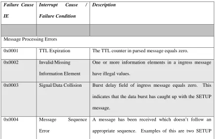
The following tables list all interrupt causes. Table 5 lists the Egress Message Ready Interrupts. Table 6
lists interrupts requesting Failure message generation and there associated Cause IE codes, while table 7
lists all other interrupt causes. Grey areas in a table indicate features that are not currently supported by
hardware.
Table 6: Egress Message Ready Interrupts
Interrupt Cause
Egress message ready at EME0
Egress message ready at EME1
Egress message ready at EME2
Egress message ready at EME3
Table 6: Hardware Failure Condition Interrupts
Failure Cause
IE
Interrupt Cause /
Failure Condition
Description
Message Processing Errors
0x0001 TTL Expiration The TTL counter in parsed message equals zero.
0x0002 Invalid/Missing
Information Element
One or more information elements in a ingress message
have illegal values.
0x0003 Signal/Data Collision Burst delay field of ingress message equals zero. This
indicates that the data burst has caught up with the SETUP
message.
0x0004 Message Sequence
Error
A message has been received which doesn’t follow an
messages with the same label or a KEEPALIVE or
RELEASE message with no prior SETUP.
0x0005 No Route to Host No Forwarding Table entry found when processing Setup.
0x0006 Connection Blocked The output port/wavelength that is needed is already being
used by a higher (or equal) QoS connection.
0x0007 Connection Unavailable This would only occur when processing a SETUP message.
In this case, all connection state machines in the IME are
being used and another connection cannot be set up at this
time.
0x0008 Burst Pre-empted An active burst was pre-empted by a higher QoS
connection.
Table 7: Other Interrupts
Interrupt Cause Description
FIFO Overflow Software attempted to overwrite an ingress message FIFO
before the IME finished reading the current message.
This error condition is detected in the RAB. The write is
not allowed to occur and the message engines are not
informed of the error.
Connection Timeout A connection has timed out. The corresponding
cross-connect must be torn down.
The RAB also communicates with the Message engine. From the perspective of the MEs, the RAB consists
of a large array of registers, some of which are inputs to ME modules and some of which are outputs from
Figure 8: RAB interface with Message engine
Status/Control IME Data
Elements
EME Data Elements
Status/Control IME0 IME1 IME2 IME3
EME0 EME1 EME2 EME3 IME Datapath
EME Datapath
RAB Message Data
Crossconnect
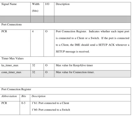
The following table 8 lists some of the configuration registers read by the IMEs from the RAB.
Table 8: IME Configuration Signals
Signal Name Width
(bits)
I/O Description
Port Connections
PCR 4 O Port Connection Register. Indicates whether each input port
is connected to a Client or a Switch. If the port is connected
to a Client, the IME should send a SETUP ACK whenever a
SETUP message is received.
Timer Max Values
ka_timer_max 32 O Max value for KeepAlive timer
conn_timer_max 32 O Max value for Connection timer.
Port Connection Register
Abbreviation Bits Description
PCR 0-3 1’b1: Port connected to a Client
0 Port 0 Connection
1 Port 1 Connection
2 Port 2 Connection
3 Port 3 Connection
4.3 Ingress Message Engine Interface (IME) Module
Ingress Message Engine (IME) module is interface module that communicates with RAB and it’s the first
stage (See figure 7) of processing messages when they are being loaded by software. When a message
arrives for a particular IME, the processor loads it into the appropriate FIFO. There is a Write Address
Pointer, which always points to the last word that was written by the processor. The IME monitors this
pointer and never reads past it.
The IME knows when it has reached the end of valid message data in the FIFO because it can parse the
message length from the beginning of the signaling message. Once the write pointer reaches the end of the
current message, it remains there until a new message is loaded. At that time it points to the beginning of
the new message data. Figure 9 below shows the logical diagram of the IME FIFO.
Control Logic wa_ptrX
read_addrX
data_reqX
in_validX [0-15]
[16-31]
in_mess X in_dataX
data_select
doneX doneX
Clock
Clock
To
IM
E
’s
0
-3
To
R
A
B
Combining stages 1 and 2, when a message arrives, it first passes through the IME. It then is fed to the
Message Parser and the CRC Checker in parallel (see figure 7). The Message Parser strips from the
message the information elements that are needed by other modules in the engine. The CRC checker
checks to make sure there are no errors in the message data. When the CRC check is complete a flag is set
to notify the rest of the modules. The value of the flag will depend on whether or not if the CRC checker
detected an error in the data or not.
4.4 Message Parser Module
The Message parser will be composed of a combinational logic block, two counters, 16 Mask Register,
Priority encoder like logic, DMUX, and an output register bank and a controller. The Parser will read 16
bits of data from the ESB/RAN every cycle. A counter will keep track of the number of bytes read so far.
The counter will tell us which part of the message is being read in the current cycle.
The Common Header will be multiplexed into the appropriate output registers. The mask will be stored in
the Mask Register. The Mask register and the length field will be used to parse the rest of the information
elements. Whenever a field is parsed and stored in the corresponding output register the appropriate valid
every element has a valid signal associated with it, which tells when the register (field) is ready to be used.
Figure 10 below shows the logical diagram of the parser module.
Figure 10: Message Parser logic diagram
At stages 1 and 2, the information elements are striped and CRC check is done to make sure there are no
errors in the message data.
4.5 CRC Checker/Generator Module
This module performs a calculation on the message data to see if there were any errors introduced during
transmission. CRC16 was implemented, and only the hard-path will be checked for errors. The CRC
Checker and CRC Generator have a similar architecture, which is basically composed of a combinational
block that will calculate the reminder of the division of the 8 bit input data by the generator polynomial. A
controller that will feedback the intermediate CRCs into the logic again along with the next 8-bit of data
And loop until the message is complete. For the CRC-Checker the controller will output a 2-bit valid signal
Indicating the status of the CRC-checker (00 ->Idle, 01 ->Valid, 10 ->Invalid, 11->Busy). For the CRC
initializes the output register to all ones (0xFFFF) to be able to detect leading zeros. Figure 11 below
shows the block diagram of the CRC-checker.
Figure 11: CRC-Checker block diagram
If the CRC detects an error, the State connection Maintenance module (SCM) reads the Call Reference of
the dropped message from and notes the reason for the drop. The SCM will then update the Register
Access Block with this information. The Register Access Block keeps running statistics of how many
messages are dropped and the reasons for these drops.
If the CRC check is passed, then other modules in the design are allowed to read in the parsed information
Elements that they need and the message is processed further.
4.6 Forwarding Engine
4.6.1 Message Engine Addressing Scheme
The message engine for Just-In-Time protocol will utilize a hierarchical addressing scheme with variable
represented by an address LV (length, Value). The length of the address is allocated 8 bits, thus allowing
maximum of 2048 bit address length.
Administrative Domain Level 1 Admin. Domain Level 2 Admin. Domain Level N
8 bits Length*8bits
Max 2048 bits
Figure 12: Proposed Addressing Structure
The idea of hierarchical addressing presumes that different administrative entities can be responsible of
assigning their part of the address hierarchy and leave to their discretion the length and further hierarchical
subdivision of address space. This is contrary to the fixed length addressing schemes, where blocks of
address must be allocated for different entities thus resulting in inefficient use of address space. Figure 13
below is the hypothetical outline of the hardware-addressing scheme in the forwarding module.
Figure 13: Domain Hierarchy
C l i e n t 1 01
0 3 0 2
0 1 0 1
0 1 N R L
M C N C L T S
N R E N D I A
0 1
0 3 0 2
C l i e n t 2 02
C l i en t 4 02 C l i en t 3
01
C l i en t 9 01
C l i e n t 1 0 02
C l i en t 7 01
C l i en t 8 02 C l i en t 5
01
C l i e n t 6 0 2 1 5 2 3 4 1
Initial design will allow four levels of address domain.
Level 1: Client node address
Level 2: Sub-domain (MCNC, NREN, ATDNET)
Level 3: Sub-domain (DIA, NRL, LTS)
Level 4: Sub-domain TOP
Each level will be assigned 8 bits of address. The forwarding engine will begin by breaking down the
address space and searching the forwarding table for the different level addresses. The following represent
domains with 8 bit wide identifiers.
Client 1: x_x_x_x_x_1_1_1
Client 2: x_x_x_x_x_1_1_2
Client 3: x_x_x_x_x_1_2_1
Client 4: x_x_x_x_x_1_2_2
Client 5: x_x_x_x_x_1_3_1
Client 6: x_x_x_x_x_1_3_2
Client 7: x_x_x_x_x_3_1_1
Client 8: x_x_x_x_x_3_1_2
Client 9: x_x_x_x_x_2_1_1
Client10: x_x_x_x_x_2_1_2
Where x = unused nibble
The minimum domain address would be a nibble (4 bit) space. Therefore, our 32-bit address could be
broken down into eight nibble wide sub-domains. Limitations must be set during administration
configuration of the domain address as the address width increases. For example if there were multiple path
from one domain to the next there would have to be a maximum number of options set. Current design
supports 7 sub-domains. Administration configuration of the forwarding tables will be handled via the
4.6.2 Forwarding Engine Configuration
There are several registers in the RAB, which store configuration information for the Forwarding Engine.
The switch address register contains the 32-bit address of the switch in which the Forwarding Engine is
located.
Once the software running on MPC8260 microprocessor configures the Register Access Block (RAB), the
forwarding tables are loaded before normal message processing can begin. During the loading process, the
contents of the forwarding tables are written to memory-mapped locations in the RAB and subsequently
stored locally within each Ingress Message Engine.
To begin the loading process, software must first load the sub-domain width registers and the switch
address register, and assert the “ft_load” flag. This flag remains asserted until all forwarding table contents
have been loaded.
The Forwarding Tables can be viewed as two arrays. There is an array of sub-domain addresses and an
array of output ports. Both arrays are 32 entries deep. This supports eight sub-domains with up to four
entries each. Table 9 below shows the forwarding table format, with entry numbers at the far right.
Table 9: Forwarding table format
Sub-Domain Table 0
Sub-Domain Table 7
Sub-domain Address Output Port
Sub-domain Address Output Port
Sub-domain Address Output Port
Sub-domain Address Output Port
Sub-domain Address Output Port
Entry 0 Entry 1 Entry 2 Entry 3
Entry 0 Entry 1 Entry 2 Entry 3
Sub-domain Address Output Port
Sub-domain Address Output Port
Sub-domain Address Output Port
4.6.3 Forwarding Engine Operation
The Forwarding Engine examines its switch address and the destination address of the message being
processed and finds the first sub-domain mismatch between the two. These sub-domain bits are then used
to access the Forwarding Table and obtain the correct output port.
Two memory blocks are used to implement the Forwarding Table in hardware. The first is a Content
Addressable Memory (CAM), which is used for address lookup. The second memory block is a RAM,
which is used for port lookup.
Two steps are needed to find the correct output port. First, the CAM is accessed using the sub-domain bits
provided by the Forwarding Engine. Inside the CAM, a comparison is made with the 4 entries in the
specified sub-domain. The CAM returns the address at which the sub-domain bits were found. This
address is then used in a read access of the RAM to retrieve the correct output port number. Figure 14
below shows the logical diagram of the forwarding engine.
Figure 14: Forwarding Engine logic diagram
Output port # Des. Addr
Source addr Addr
Data
Addr Data
Enable
Write
Sub_addr D M U X
M U X CAM0
CAM1
CAM7
Control Logic Ft load
N
The Forwarding Table has an internal structure which meets two criterion: reasonable access time by the
Forwarding Engine and efficient use of FPGA resources.
Two memory blocks are used to implement the Forwarding Table in hardware. The first is a Content
Addressable Memory (CAM), which is used for address lookup. The second memory block is a RAM that
is used for port lookup.
Two steps are needed to find the correct output port. First, the CAM is accessed using the sub-domain bits
provided by the Forwarding Engine. Inside the CAM, a comparison is made with the 4 entries in the
specified sub-domain. The CAM returns the address at which the sub-domain bits were found. This
address is then used in a read access of the RAM to retrieve the correct output port number.
The CAM and RAM have a parallel structure. Since each switch has a maximum of 4 connected ports, 4
entries are needed per sub-domain in the Forwarding Table. At eight sub-domains, there are 32 total entries
in each memory. The figure below shows how the CAM and RAM are organized.
Note that the “data” elements in the CAM are the sub-domain bits. Since the maximum sub-domain size is
32 bits, the CAM is 32 bits wide as well. For sub-domains smaller than 32 bits wide, the required numbers
of most significant bits are used for data storage. The RAM is 32 bits wide as well, so that the CAM and
RAM addresses match up and no decoding is necessary before looking up the output port number.
However, only the two most significant bits contain valid data, since that is all that is needed to represent
Table 10: Forwarding table architecture
5-bit Wide Lookup Addr
32-bit w ide Sub-domain Addresses 32 E n tr ie s Sub-domain Address Lookup (CAM) 0x00 0x01 0x02 0x03 0x1C 0x1D 0x1E 0x1F 5-bit Wide Lookup Addr 2-bit Wide Port Numbers + valid bit (LSB)
Output Port Number Look up (RAM) 0x00 0x01 0x02 0x03 0x1C 0x1D 0x1E 0x1F 32 E n tr ie s Sub-domain 0 Sub-domain 7
:
:
:
:
:
4.7 State Connection Maintenance (SCM) Module
This module can be viewed as the main controller of the whole message engine. Whenever a new message
is loaded by software into the message engine and the parser validates the information elements of the
message, the SCM sets the connection route to pass the message, adds that connection to its internal
look-up table and sets of internal timer to maintain that connection if the message is setlook-up, if the message is
keep-alive, the SCM looks its internal look-up table for valid connection, if valid connection is available, it
rolls over the keep-alive timer to its initial system timer value and maintains that connection. If the message
is release, the connection is torn down and that path is cleared for next available connection. If the message
type is failure, no connection path is setup but just will pas through the message engine. All of the above
operations are performed if the CRC check is valid. Otherwise, the message is dropped and reported to
RAB to generate interrupts.
The SCM also handles mirror cross-connect configuration table. This is a table that is inside the RAB that
message downstream or upstream. Every time a light-path is set up or torn down, the mirror configuration
must be updated.
The SCM being the biggest and most complex module of the message engine, its components include finite
state machine that keeps track of the 8 multiple connections that the SCM supports, an internal table
implemented as array of registers that hold intermediate information needed to process each message type,
combinational logic block for reporting interrupts and statistics and ability to configure the mirror cross
connection table inside the RAB.
4.7.1 Mirror Cross Connection Table
Every time a light-path is set up or torn down, the mirror configuration must be updated. There are three
circumstances in which this may happen: Setup message received & forwarded, release message received
& forwarded and when connection timeout.
When a Setup or Release message is read by software from a buffer in the RAB, there is a header at the top
of the buffer that contains cross connection information. A valid bit indicates a cross connection update
when asserted. At the same time, the SCM module updates the Mirror Cross Connection (MCC) table.
The format of the MCC Table 11 is shown below. The gray columns indicate features not supported in the
first JITPAC implementation.
Table 11: Mirror cross connection table
Mirror Cross Connection Table
1 : 1 0 : 7 X : X X : X X : X X : X 2 : 2 0 : 7 X : X X : X X : X X : X 3 : 3 0 : 7 X : X X : X X : X X : X
(MSB) (LSB) (MSB) (LSB)
For Connection Timeouts, the MCC table is updated and the processor is interrupted. The MCC table
updates that result from a Connection Timeout, ICRx[9] is asserted concurrently with the update request
signal “mcc_req1[X]”.
Update data consists of an input port number and a valid bit. For a cross-connect setup the Valid bit is set.
For a release, the valid bit is cleared. Update address is a concatenation of the output port number and the
Channel Number-1. The Channel Number is contained in the Channel Descriptor message IE. The output
port is used to index the MCC table because this ensures that no two IME’s can setup a cross connect to the
same output port on the same wavelength.
An example of an MCC update by IME0 to connect Input Port 0 with Output Port 3 using Channel 6 would
proceed as follows:
IME0 loads mcc_addr0 w/ 5’b11101
IME0 loads mcc_data0 w/ 3’b 001
IME0 asserts mcc_req[0]
MCC Arbiter asserts mcc_ack [0] and mcc_grant [0] simultaneously, for one clock cycle.
In response to an update request, the arbiter always asserts the corresponding Mcc_ack signal some time
later. If the grant signal simultaneously asserted, then the update was successful. Otherwise the update
was not made. Updates which release the cross-connect (by setting the valid bit to zero) will always be
granted. The only circumstance in which a cross-connect setup will not be granted is if there is already a
valid cross connection set up.
The tables 12 below list interface signals between the RAB and the Message Engines. The “I/O” column
indicates input/output from the RAB. The first table lists interface signals for table updates resulting from
Setup and Release message processing. The second table lists interface signals for table updates resulting
from Connection Timeouts.
The MCC Table 13 Arbiter in the RAB has one set of interface signals for each IME. There is a module
between the RAB and the IMEs called MCC mux which muxes the interface signals for Setup/Release
Updates and Connection Timeout Updates. Setup/Release Updates always have priority.
Table 12: Mirror Cross Connection Table Interface (Setup and Release Updates)
Signal Name Width
(bits)
I/O Description
IME Write Requests
mcc_req 4 I Write request signals from each IME. A request must remain
asserted until a grant is given in order for the update to be
successful.
4’bxxx1: Request from IME0
4’bxx1x: Request from IME1
4’bx1xx: Request from IME2
IME Ack/Nacks
mcc_ack 4 O Asserted for one clock cycle to acknowledge an IME’s write
request. During the clock cycle that an Ack is asserted, grant
signal for the corresponding IME is valid.
4’bxxx1: Acknowledge to IME0
4’bxx1x: Acknowledge to IME1
4’bx1xx: Acknowledge to IME2
4’b1xxx: Acknowledge to IME3
IME Grants
mcc_grant 4 O Tells the IME whether its write was granted or not.
4’bxxx1: Grant to IME0
4’bxx1x: Grant to IME1
4’bx1xx: Grant to IME2
4’b1xxx: Grant to IME3
Write Addresses
mcc_addr0 5 I Write address, IME0
mcc_addr1 5 I Write address, IME1
mcc_addr2 5 I Write address, IME2
mcc_addr3 5 I Write address, IME3
Write Data
mcc_data0 3 I Write data, IME0
mcc_data1 3 I Write data, IME1
mcc_data2 3 I Write data, IME2
Table 13: Mirror Cross Connection Table Interface (Connection Timeout Updates)
Signal Name Width
(bits)
I/O Description
IME Write Requests
mcc_req1 4 I Write request signals from each IME. A request must remain
asserted until a grant is given in order for the update to be
successful.
4’bxxx1: Request from IME0
4’bxx1x: Request from IME1
4’bx1xx: Request from IME2
4’b1xxx: Request from IME3
IME Ack/Nacks
mcc_ack1 4 O Asserted for one clock cycle to acknowledge an IME’s write
request. During the clock cycle that an Ack is asserted, grant
signal for the corresponding IME is valid.
4’bxxx1: Acknowledge to IME0
4’bxx1x: Acknowledge to IME1
4’bx1xx: Acknowledge to IME2
4’b1xxx: Acknowledge to IME3
IME Grants
mcc_grant1 4 O Tells the IME whether its write was granted or not.
4’bxxx1: Grant to IME0
4’bxx1x: Grant to IME1
4’bx1xx: Grant to IME2
4’b1xxx: Grant to IME3
mcc_addr10 5 I Write address, IME0
mcc_addr11 5 I Write address, IME1
mcc_addr12 5 I Write address, IME2
mcc_addr13 5 I Write address, IME3
Write Data
mcc_data10 3 I Write data, IME0
mcc_data11 3 I Write data, IME1
mcc_data12 3 I Write data, IME2
mcc_data13 3 I Write data, IME3
MCC Write Address
Abbreviation Bits Description
0-2 Channel Number – 1:
3’d0: Channel 1
3’d1: Channel 2
3’d2: Channel 3
3’d3: Channel 4
3’d4: Channel 5
3’d5: Channel 6
3’d6: Channel 7
3’d7: Channel 8 mcc_addrX
3-4 Output Port Number:
2’d0: Output Port 0
2’d1: Output Port 1
2’d2: Output Port 2
MCC Write Data
Abbreviation Bits Description
0 Valid bit. Indicates a valid MCC Table entry. Valid entries correspond to active
cross-connects. mcc_dataX
1-2 Input Port Number:
2’d0: Input Port 0
2’d1: Input Port 1
2’d2: Input Port 2
2’d3: Input Port 3
4.7.2 Functional And Block Diagram of The SCM
Figure 15: Functional and Block Diagram of The SCM
M U X
Combinational Logic
Internal Bank Of registers Used As table
Interrupt Logic
Statistics MCC
Table Update Logic
Table Search Logic M
U X
Output Port
Output Label Finite State
The above figure shows the complex components the SCM consists and its interactions.
4.8 Field Update Module
This module receives data that should only be updated from the parser and passes 16-bit data to the output
to Message Reassembly module. It only changes two fields the Label and TTL. If the message type is setup
the label is created in the SCM and passed to the Field Update module, if the message type is a keep-alive
the SCM looks up the label and supply it to this module FU. TTL is always decremented by one; the new
data is passed to the Message reassembly module. This module keeps track of the value of the TTL and if it
reaches zero or expires it flags and notifies the SCM to generate interrupt signals to RAB. Therefore,
failure message can be generated. Figure 16 below shows the block diagram of the Field Update module
with Message Reassembly.
Figure 16: Field Update Block diagram
Inputs from the field Update module come from the Message Parser and the State Connection Maintenance
modules.
Field Update module
ÿ
ÿ
ÿ
ÿ Message Reassembly
4.9 ACK/NACK Generation Module
The ACK/NACK module will develop the acknowledgement messages back to the node. This is the basic
novel of this protocol. Refer to the signaling definition chapter how connections are being setup and
teardown.
The ingress switch generates a Setup Ack for the client whenever a setup message is processed. The Setup
message is forwarded to the next node first. Then Setup Ack is sent to the client. The output port for a
Setup Ack is same as the input port number of the Setup message.
The Setup message is processed as usual and sent via the crossbar to the egress message buffer. There is an
IME controller, which notes that a Setup message has just been forwarded and therefore a Setup Ack
should be sent to the client. The Setup Nack also goes through the same path but the most significant bit
reversed. Table 14 below shows the setup message information elements.
Table 14: Setup Message IEs
IE Size (bits) Description
Source Address 32 Switch Address
Destination Address 32 Client Address
Label 32 Forward label from the SCM module.
Call Reference 64 From the Setup message
Channel Descriptor 64 From the Setup message
Delay Estimator 32 Unused/empty/zero’s
4.10 Output Port Requester (OPR) Module
When a message is sent to the Message engine, its parsed and all information elements are stripped from it,
address chooses which output port number will the message go through then the state connection
maintenance module creates specific connection for the message, updates the cross-connect table in RAB
and forwards the output port number to the output port number requester module.
At stage 4 of the message processing, the OPR module operates in two modes. The first is for normal
message processing. The second is for processing a Setup Ack. The only difference is which output port is
Requested. In normal mode, the output port is obtained from the SCM. In Setup Ack mode, the output
port is fixed as the IME port number. A signal indicating the current mode comes from the IME controller.
The OPR uses a "valid" signal as its request to the Crossbar. The valid signal indicates that the output port
number sent to the Crossbar is being requested. There are four grant lines, one for each output port. The
Crossbar asserts the grant line corresponding to the requested port. The OPR may have to wait for an
undefined (but finite) period of time before its request is granted.
When a request is granted, the "transmit" signal is asserted which tells the Message Reassembly module
(MRA) that it may use the Crossbar. When the Message Reassembly module is done, it asserts a "done"
signal back to the OPR. For the case when a Setup Ack should be sent, the OPR needs to return to its
default state between the Setup and Setup Ack so that it can request the new output port. During this time
the "done" signal from the MRA will go low, transmit will go low, valid will go low, & grant will go low.
However, the output port valid signal from the SCM will remain high. Therefore it is important that the
mode be switched while "done" from the MRA is asserted so that when it again goes low, the correct output
port is requested. There is great interactive and handshaking between the OPR, Message Reassembly and
Crossbar Modules.
4.11 Message Reassembly Module
This module reads the message from the RAB FIFO and transmits 32 bits at a time over the bus when it
gets a signal (transmit) from the OPR that the bus has been granted. While reading from the FIFO this