ABSTRACT
BAWA, GAURAV. A Switched Capacitor based Micro-stimulator for Deep Brain Stimulation. (Under the direction of Dr. Maysam Ghovanloo and Dr. Leda Lunardi.)
This thesis presents a novel technique for the development of an implantable stimulator for Deep Brain Stimulation. The key idea is to harvest energy from an inductive link using an efficient switching mechanism at the secondary side. To validate the concept, extensive characterization was performed by simulating explicit differential equations in MATLAB in addition to a prototype implementation in standard CMOS technology. In principle, a zero current switching methodology at the secondary coil has proved to be extremely energy efficient due to no extra wastage of power in the parallel resonant circuits.
A high efficiency full-wave rectifier has been implemented in standard CMOS technology, which ensures a measured efficiency of ~ 85 % while delivering ~ 19 mW of power to the load at 500 KHz input frequency. The underlying principle is that of synchronous rectification, minimization of MOS switch resistance through biasing in deep triode and blockage of reverse currents from the load to source using a lossless capacitive voltage divider technique.
A Switched Capacitor based Micro-stimulator for Deep Brain Stimulation
by Gaurav Bawa
A thesis submitted to the Graduate Faculty of North Carolina State University
In partial fulfillment of the Requirements for the degree of
Master of Science
Electrical Engineering
Raleigh, North Carolina 2008
APPROVED BY:
_____________________________ _____________________________ Dr. Lianne Cartee Dr. Kevin Gard
DEDICATION
BIOGRAPHY
Gaurav Bawa was born on 11th October, 1981, in Punjab, India. He received the B. Tech. in Electrical Engineering from the Indian Institute of Technology, Delhi, India in 2003. In Fall 2006, he started his graduate studies in the Department of Electrical and Computer Engineering at North Carolina State University, Raleigh, North Carolina, USA. In the summer of 2002, he was an intern in the Microelectronics Group at Universitá di Udine, Italy and in Fall 2003, at National Instruments, India, in the Motion Control Group. From 2003-2006, he worked as a Design Engineer at ST Microelectronics, India. During this period, he was involved in the design and validation of Flash Memory Test Vehicles in submicron NVM Technology, and subsequently in the design of analog-to-digital converters for the product division. His research interests include low-power RF, analog and digital circuit design.
ACKNOWLEDGEMENTS
First and foremost, I thank my parents for allowing me the freedom to choose the path less trodden and standing by me through thick and thin. To me, they are and will always be the epitomes of love, strength and integrity.
I thank Dr. Maysam Ghovanloo for providing me an opportunity to conduct research under his guidance. He is a great source of enthusiasm which is reflected in his research and teaching style. I am indebted to him for imbibing in me the mantra that “all research is quantitative”.
I would like to express my gratitude towards Dr. Leda Lunardi, for agreeing to serve as the co-chair of my committee. My sincere appreciation goes out to my very helpful and approachable committee members, Dr. Lianne Cartee and Dr. Kevin Gard. This thesis would not have been possible without the knowledge I gained in their courses. I also thank Dr. Subhashish Bhattacharya for selflessly taking out time for some intriguing technical discussions. I am grateful to Elaine Hardin for ensuring a smooth defense and graduation.
TABLE OF CONTENTS
List of Figures... vii
List of Tables ... xi
Chapter 1 ...1
1. Introduction...1
1.1 Background and Motivation ...1
1.2 Thesis Organization ...4
1.3 References...5
Chapter 2 ...6
2. System Architecture...6
2.1 Introduction...6
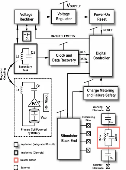
2.2 System Overview ...6
2.3 Detailed Description ...8
2.3.1 Neuron Model ...8
2.3.2 Stimulator Back-End...10
2.3.3 Charge Metering and Failure Safety Block ...11
2.3.4 Power Conditioning Block...13
2.3.5 Data Transmitter and Receiver Block...14
2.3.6 Digital Controller Block ...14
2.4 References...15
Chapter 3 ...17
3. A High Efficiency Full-wave Rectifier in Standard CMOS Technology ...17
3.1 Introduction...17
3.2 Circuit Description...18
3.2.1 Comparators ...20
3.2.2 Output Voltage Monitor...23
3.3 Measurement Results ...23
3.4 Power Dissemination in the Rectifier ...30
3.5 Limits to Rectifier Dropout Voltage ...31
3.6 Limits to Rectifier Efficiency ...32
3.7 Effects of Phase-Lead Control ...33
3.8 References...35
Chapter 4 ...37
4. An Active Rectifier with built-in dual-mode Backtelemetry in Standard CMOS Technology...37
4.1 Introduction...37
4.2 Circuit Description...39
4.3 Measurement Results ...41
4.4 Variations in loaded Q2 in different modes of operation ...46
4.5 Reflected Impedance in Backtelemetry ...51
Chapter 5 ...57
5. Analysis and Design of an Active Rectifier in Standard CMOS Technology.57 5.1 Introduction...57
5.2 Triangular Waveform Approximation ...58
5.3 Rectifier Differential Equations ...61
5.4 A comparison between methods ...64
5.5 NMOS and PMOS Switch-Size Optimization...66
5.5.1 Minimizing Area for a given Switch Resistance ...68
5.5.2 Minimizing Switch Resistance for a given Area ...70
5.6 A High Frequency Rectifier in Standard CMOS Technology ...73
5.7 References...77
Chapter 6 ...79
6. Design of a Switched Capacitor Based Microstimulator...79
6.1 Motivation...79
6.2 System Specifications ...80
6.3 Fundamental Theory of Operation...80
6.4 Charging via Parallel RLC Tank...82
6.4.1 Simulation Results ...84
6.4.2 Theoretical Analysis of Efficiency ...89
6.4.3 Comparison with a Parallel RLC Rectifier ...91
6.5 Charging via Series RLC Tank ...97
6.5.1 Simulation Results ...100
6.6 Proof of Concept ...107
6.7 References...114
Chapter 7 ...116
7. Conclusions and Future Work...116
7.1 Conclusions...116
LIST OF FIGURES
Fig. 1.1 An implantable cardiac pacemaker device ...1 Fig. 1.2 Examples of highly size constrained IMDs (a) Intraocular Epi-retinal
Prostheses and (b) Cochlear Implant ...2 Fig. 1.3 A state-of-the-art implanted deep brain stimulator...3 Fig. 2.1 Simplified Architecture of a contemporary wirelessly-powered Implantable
Stimulator System ...7 Fig. 2.2 (a) Neuron Model (b) Response of neuron to a stimulus ...9 Fig. 2.3 A typical charge-balanced biphasic current stimulus pulse ...12 Fig. 3.1 Complete rectifier schematic including the inductive-link used for telemetry
power transmission ...18 Fig. 3.2 Comparator schematic representing the gray dashed box in Fig. 3.1...20 Fig. 3.3 Simulation results showing the coil voltages (VC1 and VC2), divided C1
voltage (VC1D), gate and bulk voltages for P1 (VGC1 and VBC1, respectively), and the output voltage (VOUT) ...21 Fig. 3.4 (a) Schematic diagram of the output voltage monitor. (b) Post-layout
transient simulation of the rectifier waveforms at startup ...24 Fig. 3.5 Die Photo of the rectifier in AMI 0.5 µm CMOS process ...25 Fig. 3.6 Measured rectifier input and output waveforms when VC1,2(peak) = 5 V, RL =
1 kΩ and CL = 1 µF ...25 Fig. 3.7 Measured rectifier PCE and output DC voltage when VC1,2(peak) = 5 V and
CL = 1 µF as a function of input carrier frequency (f ) with output loading
(RL) of 1 kΩ...27 Fig. 3.8 Measured output DC voltage when VC1,2(peak) = 5 V and CL = 1 µF as a
function of RL with f = 0.5 MHz ...27 Fig. 3.9 Waveforms of a rectifier during the half-wave with time stamps indicated .29 Fig. 3.10 Pie-chart showing the simulation results of the distribution of input power in
the Rectifier at maximum efficiency (90.4%) and nominal loading of RL = 1 kΩ. V2= 5 V, f = 0.5 MHz, and CL = 1 µF ...31 Fig. 3.11 Simulated rectifier PCE and output DC voltage vs. RL when ideal
comparators (A1,2) are used in the rectifier of Fig. 2 (compare with Fig. 5b). Operating conditions: VC1,2(peak) = 5 V, f = 0.5 MHz, CL = 1 µF ...32
Fig. 3.12 PCE variation vs. comparator delay, Td, at 1 MHz with and without phase-lead compensation using a capacitive divider with the voltage division ratio shown on the left vertical axis. The capacitive divider is added to the input of the comparator to control the reverse current ...34 Fig. 3.13 PCE variations vs. phase-lead division ratio, σ = CPOLY/(CPAR + CPOLY), for a
fixed comparator delay of Td = 10 ns when VIN= 5 V at 1MHz ...35 Fig. 4.1 Block diagram of a generic system for wireless power and data transmission
across an inductive link. ...38 Fig. 4.2 Complete active back-telemetry rectifier (ABTR) schematic for forward
Fig. 4.3 Die photo of the active back telemetry rectifier chip fabricated in AMI 0.5-µm standard CMOS process (0.45 × 0.9 mm2) ...42
Fig. 4.4 Measured ABTR waveforms showing consecutive OC, Rectifier, and SC modes of operation at f = 1 MHz, CL = 144 nF and RL = 1 kΩ...43 Fig. 4.5 Waveforms showing (from top) the original and Manchester-encoded data bit
streams, primary sensed current, carrier envelope, and recovered back
telemetry data, which was sent through the ABTR OC input at 200 kHz with f = 1 MHz, RL = 1 kΩ and d = 20 mm ...44 Fig. 4.6 Simplified and linearized equivalent circuit description for the inductive
wireless link shown in Fig. 4.2 ...47 Fig. 4.7 Imaginary, real, and magnitude of the transponder impedance, Z2, and its
loaded quality factor, Q2L, vs. the linearized resistance seen through ABTR input port RL, eq in Fig. 4.6...52 Fig. 4.8 The reflected impedance (ZR) at the primary shown in the complex plane as a
function of equivalent loading at the secondary (RL,eq), with RL,eq ascending from left to right in the range 1 Ω – 1 kΩ ...53 Fig. 5.1 Equivalent Circuit model of a half-wave rectifier ...58 Fig. 5.2 Triangular approximation of the VOUT steady state ripple waveform during
charging and discharging phases of CL when the rectifier switch closes and opens with duty cycle, D, in every carrier cycle, TS = 1/f. The same model applies to full-wave rectifiers if VIN is commutated and TS = 1/2f ...59 Fig. 5.3 Half-wave rectifier waveforms generated in MATLAB based on more
realistic differential equations setup in section 5.3 to find the relationship between switching duty cycle, D, and other circuit parameters in Fig. 5.1. VIN = 5 V, f = 1 MHz, RS= 5 Ω, RL= 1 kΩ, and CL= 1 nF ...62 Fig. 5.4 Plot of f(D), defined in section 5.3, with zero crossing at D = 0.21 for VIN =
5 V, f = 1 MHz, RS= 5 Ω, RL= 1 kΩ, and CL= 1 nF in Fig. 5.1...64 Fig. 5.5 Comparing closed form approximation, numerical differential equations, and
SPICE simulation methods for evaluating the rectifier PCE vs. RL. Nominal values are CL = 1 µF, RL = 1 kΩ, and RS = 5 Ω...65 Fig. 5.6 Comparing closed form approximation, numerical differential equations, and
SPICE simulation methods for evaluating the rectifier PCE vs. CL. Nominal values are CL = 1 µF, RL = 1 kΩ, and RS = 5 Ω...66 Fig. 5.7 Comparing closed form approximation, numerical differential equations, and
SPICE simulation methods for evaluating the rectifier PCE vs. RS. Nominal values are CL = 1 µF, RL = 1 kΩ, and RS = 5 Ω...67 Fig. 5.8 Plot showing the variation of the total switch resistance, RS, with the choice
of the width of the PMOS transistor, for a given area constraint of A = 2500 µm2 in AMI-0.5 µm standard CMOS technology (Table 5.1) ...72 Fig. 5.9 SPICE simulation results showing the variation of PCE and VOUTvs. the
Fig. 5.10 SPICE simulation results showing the variation of PCE and vs. the PMOS switch size (WP) at an operating frequency of 13.56 MHz, in a full-wave IC-rectifier with ideal comparators in 0.5-µm CMOS technology. The NMOS switches are driven dynamically in this case ...74 Fig. 5.11 Schematic of a full-wave rectifier core operating at ISM Band frequency ..75 Fig. 5.12 A high speed asynchronous comparator driving the NMOS switch in a
full-wave rectifier operating at f = 13.56 MHz ...76 Fig. 6.1 Circuit Description and step response of charging a capacitor with (a)
Constant Voltage Source (b) Constant Current Source ...81 Fig. 6.2 Circuit Schematic showing the concept of a half-wave Parallel SCS ...83 Fig. 6.3 MATLAB simulation of a half-wave Parallel SCS, when f = 1 MHz, L2=
7.77 µH, R2= 4.975 Ω, C2 = 3.26 nF, CLP= 1 µF, TSW = 50 ns, VIND = 0.35 V 86
Fig. 6.4 Efficiency and Energy Profile in MATLAB of a half-wave Parallel SCS, when f = 1 MHz, L2= 7.77 µH, R2= 4.975 Ω, C2 = 3.26 nF, CLP= 1 µF, TSW =
50 ns ...88 Fig. 6.5 Circuit Schematic showing the concept of a full-wave Series SCS. The
control circuitry is not shown ...97 Fig. 6.6 MATLAB simulation showing the voltage profile during switching of a
full-wave Series SCS, when f = 1 MHz, L2= 3.05 µH, R2= 0.53 Ω, C2 = 8.3 nF, CLP,N= 1 µF, VIND = 5 V ...98 Fig. 6.7 MATLAB simulation of a full-wave Series SCS, when f = 1 MHz, L2= 3.05
µH, R2= 0.53 Ω, C2 = 8.3 nF, CLP,N= 1 µF, VIND = 5 V. (a) Input and output voltages (b) Input inductor current ...99 Fig. 6.8 MATLAB simulation results showing the dependence of efficiency and
output DC voltage on R2 in a full-wave Series SCS, when f = 1 MHz, L2= 3.05 µH, C2 = 8.3 nF, CLP,N= 1 µF, VIND = 5 V ...100 Fig. 6.9 MATLAB simulation of a full-wave Series SCS, when f = 1 MHz, L2= 3.05
µH, R2= 0.53 Ω, C2 = 4 nF, CLP,N= 1 µF, VIND = 5 V. (a) Input and output voltages (b) Input inductor current ...101 Fig. 6.10 MATLAB simulation results showing the dependence of efficiency and
output DC voltage on R2 in a full-wave Series SCS, when f = 1 MHz, L2= 3.05 µH, C2 = 4 nF, CLP,N= 1 µF, VIND = 5 V ...102 Fig. 6.11 MATLAB simulation results showing the dependence of (a) efficiency and
output DC voltage (b) charging time, on C2 in a full-wave Series SCS, when f = 1 MHz, L2= 3.05 µH, R2= 0.53 Ω, CLP,N= 1 µF, VIND = 5 V ...103 Fig. 6.12 MATLAB simulation results showing the dependence of efficiency and
output DC voltage on f in a full-wave Series SCS, when L2= 3.05 µH, C2 = 4 nF, R2= 0.53 Ω, CLP,N= 1 µF, VIND = 5 V ...104 Fig. 6.13 MATLAB simulation results showing the dependence of (a) charging time
Fig. 6.14 MATLAB simulation results showing the dependence of efficiency on C2 and CLP,N in a full-wave Series SCS, when f = 1 MHz, L2= 3.05 µH, R2 = 0.53 Ω, VIND = 5 V ...106 Fig. 6.15 Schematic of PMOS based switch for implementing the switch for (a) CLP
(b) CLN ...109 Fig. 6.16 Schematic of NMOS based switch for implementing the switch for (a) CLP
LIST OF TABLES
Table 4.1 Active Back Telemetry Rectifier Modes of Operation...41 Table 4.2 Q2L and RL,EQ Variations in various modes of rectifier operation ...51
Chapter 1
1.
Introduction
1.1Background and Motivation
With the advent of integrated circuit technology, the miniaturization of complex computing systems such as microprocessors occurred as a natural consequence which revolutionized the way the common man perceived these large processing machines. Towards the later part of the 20th century, the miniaturization due to the silicon technology and its biocompatibility resulted in advancement of medical electronics. This occurred simultaneously with the advancement in neurophysiology. In late 1950s, the development of integrated cardiac pacemakers took place, whose basic purpose is to
Fig. 1.2. Examples of highly size constrained IMDs (a) Intraocular Epi-retinal Prostheses [2] and (b) Cochlear Implant [3].
(a) (b)
ensure that heart beats at the correct rate and rhythm. Thus, in such a device, the circuitry for both the recording/processing and generation of the cardiac action potentials is necessary. Fig. 1.1 shows the example of a state-of-the-art pacemaker device, in which a battery is present to supply DC power to the on-chip circuitry, which has a lifetime of 10 ~ 12 years, made possible through ultra-low-power design techniques [1].
In the last few decades, researchers have been working towards more ambitious goals like cochlear implants and retinal prostheses for aiding the deaf and blind respectively (see Fig. 1.2). Due to size constraint in these applications, it is not possible to have a small enough battery present with the implant, which can ensure a lifetime similar to that in the case of pacemakers. In such scenarios, the power transmission needs to be done wirelessly since the implant needs to be minimally invasive. This is
battery while the secondary coil converts the variations in magnetic flux to electrical
signals and is made available to a rectifier which performs AC-DC conversion to power
the stimulator or recording circuitry. The complete system needs to be extremely
energy-efficient to maximize the life and minimize the size of the external battery, and to
minimize the internal power dissipation which can raise the temperature of the implant.
The exact value depends on the location of the implant inside the body, but as a
thumb-rule, it should not result in an increase of temperature of the surrounding tissue by more
than 1 °C [4].
Deep brain stimulation is a commercially available effective therapy for patients suffering from movement disorders like Parkinson’s disease, Tremor and Dystonia. These devices being inspired by the pacemaker technology are currently
implanted in the chest area of the patient, as shown in Fig. 1.3. The wires connecting the stimulator device to the implanted electrodes run through the back of neck and result in mechanical failures due to strain developed over a period of time. This is the case since these stimulators are not efficient enough to result in a smaller battery, which consumes half the area of the total implanted device. The ultimate goal of this research is to provide energy-efficient solutions in wireless power transmission to take the battery out of the system, leading to considerable size reduction. Hence, it would be possible to fit the device outside the skull, under the scalp leading to minimal invasiveness, reduced patient discomfort and an enhanced robustness.
In addition to the power transmission, there is a need for data transmission from the implant. This is important for the doctor to be able to adjust the stimulation parameters, to set up a feedback loop or to know the status of the implanted device. The same principle is applicable in passive Radio-Frequency-Identification (RFID) systems, in which the reader wirelessly powers the transponder through an alternating carrier and performs identification by sending data back and forth on the same carrier signal [6]. More recently, researchers are looking at efficient means of energy harvesting in micro-power applications for use in wireless sensor nodes [7].
1.2Thesis Organization
describes the theory and implementation of complementary Backtelemetry features in an active rectifier leading to an enhanced reading range. Chapter 5 provides the analysis and design guidelines for an active full-wave rectifier in standard CMOS technology. Chapter 6 describes the theory and proof-of-concept for an energy-efficient switched capacitor based microstimulator. Finally, Chapter 7 contains the conclusions of the thesis with scope for future work.
1.3References
[1] L.S.Y Wong et al., “A very low power CMOS mixed signal IC for implantable pacemaker applications”, IEEE J. Solid State Circuits, vol. 39, pp. 2446 – 2456, Dec. 2004.
[2] http://www.nsf.gov/od/lpa/news/03/pr03115.htm [3] http://www.nidcd.nih.gov/health/hearing/coch.asp
[4] G. Lazzi, “Thermal effects of bioimplants,” IEEE Eng. in Med. Biol. Magazine, vol. 24, no. 5, pp. 75-81, Sep. 2005.
[5] S.K. Moore, “Psychiatry's shocking new tools”, IEEE Spectrum, Vol. 43, Issue 3, pp. 24 - 31, Mar. 2006.
[6] K. Finkenzeller, RFID-Handbook, 2nd Ed., Wiley, Hoboken, NJ, 2003.
[7] T.T. Lee et al., “Piezoelectric Micro-power generation interface circuits”, IEEE J. Solid State Circuits,
Chapter 2
2.
System Architecture
2.1Introduction
In this chapter, we describe a system level architecture for
size-constrained implantable microelectronic devices (IMD) that do not have a built-in
battery, and are hence wirelessly powered. As discussed in Chapter 1, this is indeed true
for applications like bionic ears and epi-retinal prosthesis. Since the larger objective of
this research is to eliminate a battery in a conventional Deep Brain Stimulation implant
by employing efficient energy harvesting techniques from an inductive link, the resultant
stimulator architecture will also be applicable to DBS.
2.2System Overview
With the battery absent from the implanted system, the power
requirements need to be met by wireless power transmission through a pair of
magnetically coupled coils, which must be placed close to each other at a distance of a
few centimeters, depending on the nature of application. This is done in order to increase
the coefficient of coupling (k) between the coils and hence maximize the efficiency of the
link.
A generic architecture of such a system is shown in Fig. 2.1. The complete
system consists of components that are either external to the body or implanted inside
the body. The latter can either be implemented on an integrated circuit (IC) or be
tradeoff. While an integrated circuit helps in reduction of size, it comes with a cost
overhead. Hence, the components which do not show appreciable reduction in size on
migration to an IC should preferably be implemented as a discrete component.
2.3Detailed Description
In this section, we will have a closer look at the components and their
specifications. The sub-division has been done based on the functionality and deliberately
done with a bottom-top approach to understand the system conception. To begin with, a
generic neuron electrical model is presented to understand the target load driven by the
system.
2.3.1 Neuron Model
Fig. 2.2 (a) shows the Hodgkin-Huxley model for a cell membrane based
on the observations from the voltage-clamp experiments conducted on a squid axon [1].
CMEMis the capacitance of the membrane which physically exists due to the separation of
two conducting mediums with different concentrations. The ionic contributions of
Sodium (Na+), Potassium (K+) and Chlorine (Cl-) diffusion currents is modeled by the
conductance gNA, gK and gCL in series with their respective Nernst Potentials [2]. When
the membrane is at equilibrium and no current flows through CMEM, the membrane rest
potential is given by,
CL K NA
CL CL K K NA NA REST MEM
g g g
E g E g E g V
+ +
+ +
=
(b)
The Nernst Potentials for potassium and chlorine are negative while that of sodium is
positive. The resulting rest potential of the membrane is typically ~ - 70 mV.
Fig. 2.2 (b) shows the response of a neuron to a stimulus. If the magnitude of the stimulus is so small that it is unable to depolarize the cell membrane a threshold voltage above its resting potential, then no action potential will occur. In this case, the response resembles that of a parallel RC charging and discharging profile. Once the threshold is exceeded, the sodium activation channels begin to open leading to a greater influx of Na+ ions from extracellular to intracellular medium, leading to cell membrane depolarization. At the peak of the curve, the sodium inactivation channels close leading to a period of refractoriness. At this point, K+ ions begin to leave the cell due to the activation of their gating channels which leads to a decrease in the membrane potential. This eventually results in a period of hyperpolarisation before the cell membrane reaches its resting potential [2]. This variation in the ionic conductance over time is represented by a variable resistance in the electrical model in Fig. 2.2 (a), resulting in a non-linear load for the stimulator.
2.3.2 Stimulator Back-End
There can be multiple sites present in a given stimulator depending on the type of application, and the number of the sites active at any given time is generally programmable. In addition, the stimulation can either be Monopolar or Bipolar. In Monopolar stimulation, the charge is injected in the extracellular medium using a given working electrode while the charge is returned to a distant ground reference, which can be made as the body of the stimulator. In this case, the stimulating site can be modeled as a point source generating spherical equipotential surfaces around it, making it non-directional. In Bipolar stimulation, the working and the counter electrode are placed in close proximity, such that the current passing through one is returned through the other electrode. This ensures a greater degree of selectivity in stimulation since the electric field distribution is concentrated. In Fig. 2.1, the example shown is that of bipolar stimulation, with the electrodes modeled by their equivalent double layer capacitance, CDL [4]. In addition, these electrodes are shown to be integrated since they can be fabricated on silicon substrates along-with the CMOS circuitry, also known as micro-machined electrodes [5]. This ensures complete integration of the entire system resulting in an extremely compact footprint.
2.3.3 Charge Metering and Failure Safety Block
pulses are used for stimulation for charge balancing. This means that an anodic phase always follows a cathodic phase or vice-versa (Fig. 2.3). There exist safety limits based upon the amount of charge injected into the tissue per stimulus phase (QPH) and charge density of the microelectrode (QD) [6]. Thus, a biocompatible electrode with high charge carrying capability should be the choice for this application. Typically, Iridium Oxide or Tantalum electrodes since they display the aforementioned characteristics [7].
Typically, the stimulators used are either voltage-controlled (VCS) or current-controlled (CCS). In VCS, the amount of charge injected into the tissue is not controlled and hence there is a need for charge metering. One method is to measure the charge injected by
integrating the current flowing into the electrode over time. This analog information can be converted to digital domain by the use of a precision low-power Analog-to-Digital Converter (ADC). The binary data bits thus obtained can be used to communicate to the central control system and be stored on-chip for data-logging. Even in the case of CCS, to ensure that the net charge injected is zero is practically not possible. This is because, the
current injected in the cathodic and anodic phases is limited by the mismatch between the transistors and hence a technology dependant parameter which of the order of ~ 1 – 2 %. One simple way to achieve this is by shorting the electrode after stimulation, the accuracy of which is constrained by the switch resistance, the double layer capacitance and the frequency of stimulation. For stimulators requiring higher matching, especial circuit techniques need to be utilized [8].
Failure safety is an important feature of an implantable stimulator. This is
because, if a device failure takes place, it must be ensured that an uncontrollable amount of charge is not injected into the tissue. This can be heuristically ensured by evaluating faults such as junction and oxide breakdowns and generating appropriate status signals on the chip [9].
2.3.4 Power Conditioning Block
The most important block in the complete system is the one ensuring the
power transfer since power efficiency is one of the most important factors in biomedical
implants. In a typical wirelessly powered system as shown in Fig. 2.1, the battery is
present external to the human body providing stable DC supply to a switch-mode class-E
power amplifier (PA). It is desirable to maximize the efficiency to maximize the battery
life and reduce its size, and most importantly to minimize the power dissipated in the
tissue. The PA powers the primary inductor (L1) which is loosely coupled to a secondary
coil (L2), implanted inside the body. Since the size of L2 cannot be made very large, the
transmission efficiency. The AC power received at the secondary is converted to DC by
an integrated voltage rectifier, which is generally followed by a low-dropout voltage
regulator (LDO) to provide high frequency switching noise free stable supply, VSUPPLY.
As can be seen from Fig. 2.1, this supply is made available to rest of the on-chip
circuitry. A power-on-reset circuit present after the voltage regulator detects a stable
value of VSUPPLY, and resets the state machine in the digital control logic.
It must be understood that the bottleneck in power transmission efficiency
in mainly the coupling of the inductors, the voltage rectifier and finally the stimulator
block. The focus of this work is mainly on the rectifier and stimulator blocks as will be
covered in later chapters.
2.3.5 Data Transmitter and Receiver Block
There is a need for forward data transmission from the external world to
the implanted system. This is mainly to allow the programmability of the stimulation
parameters, since the doctor needs to adjust them for a certain individual. The forward
data is generally produced by modulating the carrier at the transmitter and the receiver
implemented on-chip for demodulating the data and clock extraction from the same.
In addition, there can be a need to transmit data back to the external world
which could include status of the implant temperature (sensors not shown in Fig. 2.1), a
failure status or send back the data logged during stimulation. This is generally achieved
by a low data rate backtelemetry which can be incorporated in the voltage rectifier, as
2.3.6 Digital Controller Block
The digital controller module forms the brain of the implant, making sure
that the system works in a proper order both in terms of handshaking between the various
on-chip components and that with the external world. It is fairly inexpensive in terms of
power requirements since there is no need for a very high speed operation in such an
application. The implement should preferably be custom ASIC design as against a
reconfigurable logic in order to optimize the design for area and power. In addition,
several low-power digital design techniques can also be used, if the frequency of
operation is not high [10].
2.4References
[1] A. L. Hodgkin, A. F. Huxley and B. Katz, “Measurement of current-voltage relations in the membrane of the giant axon of Loligo”, J. Physiol., vol. 116, pp. 424-448, 1952.
[2] R. Plonsey and R.C. Barr, “Bioelectricity: A Quantitative Approach”, 2nd ed., Kluwer Academic Publishers, 2000.
[3] http://media.wiley.com/assets/7/95/0-7645-5422-0_0704.jpg
[4] D.R. Merill et al., “Electrical stimulation of excitable tissue”, Journal of Neuroscience Methods, pp. 171-198, 2005.
[5] K. D. Wise et al., “Wireless Implantable Microsystems: High-Density Electronic Interfaces to the Nervous System”, IEEE Proc., vol. 92, no. 1, pp. 76 – 92, Jan. 2004.
[6] A.M. Kuncel and W.M.Grill, “Selection of stimulation parameters for deep brain stimulation”, J. of Clinical Neurophysiology, pp. 2431– 2441, 2004.
[8] J.J. Sit and R. Sarpeshkar, “A low-power blocking capacitor free charge balanced electrode stimulator chip with less than 6 nA DC error for 1 mA full-scale stimulation”, IEEE Trans. Biomed. Cir. and Sys., vol. 1, no. 3, pp. 172 – 183, Sep. 2007.
[9] X. Liu, A. Demostheneous and N. Donaldson, “A stimulator output stage with capacitor reduction and failure-checking techniques”, IEEE Intl. Symp. Cir. Sys., pp. 2076 – 2079, May 2006.
Chapter 3
3.
A High Efficiency Full-wave Rectifier in Standard CMOS
Technology
3.1Introduction
triode region as well as decreasing the reverse and substrate leakage currents. We also ensure the rectifier safe startup by employing a supporting parallel path.
3.2Circuit Description
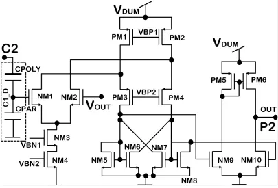
A generic inductive link for power transmission including a simplified schematic of the proposed rectifier is shown in Fig. 3.1. Instead of diode-connecting the main rectifying PMOS transistors (P1, P2) as in our prior work [5], a pair of comparators is used to sense the difference between the input coil voltages (VC1, VC2) and the rectified output (VOUT) across each rectifying PMOS. The comparator outputs switch P1 and P2 On
or Off depending on whether VC1,2 are greater or lesser than VOUT, respectively. When the comparator outputs are low, VSG1,2 ≈ VC1,2 > (VSD1,2 + |VTP|), where VTP is the PMOS threshold voltage. As long as VOUT > |VTP|, P1 and P2 are pushed into deep triode region
where they are On and produce a much smaller dropout along the main current path to the load, RL, compared to when they are in saturation. Similarly, N1 and N2 experience a large
VGS1,2 = VC1,2 > VTN when they are On and, therefore, show a small dropout in the current return path from RL back to the LC-tank. P1~5have been implemented in separate n-well regions and their bulk voltages are dynamically controlled using auxiliary PMOS devices (P1A, P1B) to eliminate body-effect and substrate leakage. While the former prevents the threshold voltage of the rectifying transistors from increasing, hence reducing the dropout voltage, the latter reduces the risk of latch-up [5]. Both of these effects also help improving the rectifier PCE.
dummy rectifier Off. In the rest of this section we describe the details of the rectifier operation, some of the design issues, and post-layout simulation waveforms.
3.2.1 Comparators
In this topology (Fig. 3.1), the most important block that determines the rectifier performance is the comparator. Two-stage hysteresis comparators were designed (Fig. 3.2) using partial positive feedback [6] with an input common-mode range (ICMR)
that extends beyond the supply level by utilizing an NMOS folded cascode differential pair. An output stage is also added to provide rail-to-rail output swing as well as high
speed drive capability of the large P1,2 capacitive gate terminals (W/L = 2.5mm/0.6µm).
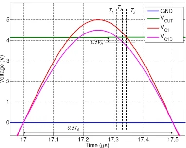
Hysteresis is important for this application to reject noise and interference at the input of the comparators and to reject the dip in the input coil voltage when P1,2 are activated.
This dip is due to the fact that when current passes through P1, the return current through
N2 causes C2 to become slightly negative and consequently decreases C1. This effect is
illustrated in the simulation in Fig. 3.3.
A supply-independent bias for the comparator is provided by a beta multiplier, which is designed to provide a current of 2 µA at 2.5 V supply. Both the bias generator and the comparator are connected to VDUM to quickly start up and initiate the rectification process. There exists a possibility of back current propagation from the ripple-rejection capacitor, CL, back to the coil when VC1,2 < VOUT and the comparator
Fig. 3.3. Simulation results showing the coil voltages (VC1 and VC2), divided C1 voltage (VC1D), gate and bulk voltages for P1 (VGC1 and VBC1, respectively), and
tends to switch P1,2 Off. This current, which can reduce the rectifier PCE by stealing the
stored charge from CL, results mainly from the finite delay associated with the comparators. Increasing the comparators speed would be helpful only up to a certain level at the cost of increased power consumption, which also harms the PCE. Our remedy was to create a phase-lead and initiate an early comparison by utilizing lossless capacitive voltage dividers at the negative input terminal of each comparator, as illustrated in Fig. 3.2. The small phase-lead will compensate for the comparator delay both at the onset of P1,2 turn-on and at turn-off. Capacitive dividers have an insignificant effect on the
LC-tank resonance frequency, which can be accounted for by adjusting CP value.
The capacitive division is achieved by using a poly-poly capacitor, CPOLY, and the input gate capacitance of the folded cascode NMOS, CPAR, as shown in Fig. 3.2. Even though CPARis highly nonlinear, since the P1,2 switching mainly takes place when
the coil voltages are high, we can expect CPAR to show a constant gate capacitance in the strong inversion region. Care must be taken to ensure that the bottom plate of CPOLY is connected to the input coil nodes and not to the floating input node of the comparator. In this design, the comparator delay and hysteresis, and the capacitive divider work in synergy to prevent any reverse current from propagating back to the coil. Disruptions in this balance can lead to decreased PCE. Therefore, a tuning mechanism would be desirable. For example, PCE would be lowered by an increased comparator hysteresis that delays P1,2 firing. The effect of capacitive voltage divider is more complicated. An
increased ratio would mean that P1,2 turn On early and turn Off late. This will lead to
waveforms in Fig. 3.3 show the comparator action with VOUT and VC1D being the comparator inputs and VGC1 as its output.
3.2.2 Output Voltage Monitor
The comparators are initially powered by the dummy rectifier path (P3,4)
to quickly become functional and start the main rectifier. However, once the main rectifier starts up, VOUT surpasses VDUM due to its smaller dropout voltage and it would be necessary to supply the comparators from VOUT to extend their input dynamic range. A simple circuit, shown in Fig. 3.4 (a), which has no static power consumption [7], monitors VOUT and once it surpasses a certain threshold (2VTP), activates a one-shot circuit to turn P5 On after a certain delay (RMCM). Note that the last inverter in the chain must be supplied by VDUM since during the time when VOUT is not yet stable, P5 needs to
be kept Off by the only stable voltage present on chip, which is VDUM. The rectifier startup is simulated in Fig. 3.4 (b). It can be seen that VDUM rises rapidly up to ~3.5 V. However, VOUT catches up in about 20 µs and the output monitor turns P5 On, shorting
VDUM to VOUT. This automatically turns the dummy rectifier (P3,4) Off.
3.3Measurement Results
(b)
Fig. 3.4. (a) Schematic diagram of the output voltage monitor. (b) Post-layout transient simulation of the rectifier waveforms at startup.
Fig. 3.6. Measured rectifier input and output waveforms when VC1,2(peak) = 5 V, RL = 1 kΩ and CL = 1 µF.
carrying P1,2 and N1,2 transistors and equipped them with guard rings to reduce the risk of
latch-up and substrate leakage [5]. The rectifier occupies ~0.4 mm2 in this process. To test the rectifier, we setup an inductive wireless link similar to Fig. 3.1 using a pair of planar spiral coils with primary and secondary inductances of 24.3 and 14.8 µH, respectively. The relative distance between the coils was 10 mm, about the average thickness of the skin, and their geometries were optimized for operation at 1 MHz as described in [9]. The coupling coefficient between the coils when they were aligned was measured k≈ 0.25 using a network analyzer (Agilent E5071B). L1 was driven by an HP 8111A function generator, and measurements on L2 were done using a multichannel digital oscilloscope (Tektronix DPO-4034). Fig. 3.6 shows the measured rectifier waveforms when VC1,2(peak) = 5 V, f = 0.5 MHz, and the rectifier is loaded with RL || CL = 1 kΩ || 1 µF.
Fig. 3.8. Measured rectifier output DC voltage when VC1,2(peak) = 5 V and CL = 1
µF as a function of input carrier frequency (f ) with output loading (RL) of 1 kΩ.
Fig. 3.7. Measured rectifier PCE and output DC voltage when VC1,2(peak) = 5 V and CL = 1 µF as a function of input carrier frequency (f ) with output loading (RL) of 1
hence decreasing the PCE.
To understand Fig. 3.7 in more detail we have performed the following simple analysis, see Fig. 3.9.
VOUT= Output DC Voltage (V)
TD = Regeneration Time constant of the comparator (sec) VH = Hysteresis Window of the comparator (V)
ω0 = Input sinusoidal frequency (rad/sec) Vi = Input Voltage Amplitude (V)
K = Input Voltage Capacitive Division factor
T2 = Time instant when VOUT becomes equal to the input voltage (sec)
T1 = Time instant when VOUT becomes equal to the divided input voltage (sec)
T3 = Time instant when (VOUT - VH/2) becomes equal to the divided input voltage and
the comparator enters into the regenerative mode (sec) From the above definitions, we can write:
3 2 T T
TD= − (3.3.1)
× = − i OUT KV V T 1 0 1 1 sin
ω
(3.3.2) × = − i OUT V V T 1 0 2 sin 1ω
(3.3.3) − × = − i H OUT KV V VT 1 sin 1 2
0 3
ω
(3.3.4)
−
−
×
= − −
i H OUT
i OUT D
KV V V V
V
T 1 sin 1 sin 1 2
0
ω
(3.3.5)
Eq. (3.3.5) is a relation between the comparator delay, hysteresis, capacitive division, input voltage frequency and amplitude as well as the output DC voltage. VOUT, however, is still a dependant parameter, while the others can be chosen by design. Thus, each one of them affects VOUT and consequently the PCE in a non-linear fashion. This also makes the design optimization of the comparator extremely complex and needs to be done empirically through simulations.
3.4 Power Dissemination in the Rectifier
A post-layout simulation of the ABTR circuit in Fig. 3.2 was performed to analyze the power distribution in various power dissipating elements in the Rectifier mode when it provides the maximum PCE based on the measurements (V2= 5 V, f = 0.5 MHz, CL = 1 µF, and RL = 1 kΩ). Fig. 3.10 shows the result of this simulation in a pie-chart. The rectifier PCE, obtained by dividing the power delivered to the load by the total input power, was 90.4%, which is 5.6% higher than the measured value in Fig. 3.7. We believe that this discrepancy was resulted from the additional parasitic components, which were not included in the rectifier model, especially those from interconnects and measurement instrumentation. In a real application, such as in Interestim-2B [2], since the rectifier block is going to be part of a system-on-a-chip (SoC), its efficiency is likely to be closer to the higher simulated value.
capacitance of these switches. Hence, there needs to be a compromise between the rectifier size, comparator drive capability, and carrier frequency, which is out of the scope of this paper. A detailed theoretical analysis and optimization of the active integrated CMOS rectifiers can be found in Chapter 5 of the thesis.
3.5Limits to Rectifier Dropout Voltage
As mentioned in section II, we have introduced a phase-lead when P1,2 is being switched Off to account for the comparator delay and eliminate reverse currents [14], [18]. On the other hand, the loss-less capacitive divider also introduces a phase-lag when P1,2 is being switched On. The comparator delay also adds to this lag and results in a notable reduction in the switching duty cycle. In the present design, for example, the input capacitive divider has a ratio of 0.93, which corresponds to a 350 mV dropout
Fig. 3.10: Pie-chart showing the simulation results of the distribution of input power in the Rectifier at maximum efficiency (90.4%) and nominal loading of
RL = 1 kΩ. V2= 5 V, f = 0.5 MHz, and CL = 1 µF.
Power Dissipation
Breakup
90.4
1.02
0.02
1.17
7.4
voltage at 5 V input. Thus, a lower dropout can be achieved in this architecture by employing a faster comparator and reducing the phase-lead accordingly.
3.6Limits to Rectifier Efficiency
In active rectifiers the comparator characteristics such as delay, power consumption, and output drive capability have a significant effect on the maximum achievable efficiency. To observe the effect of comparator delay on efficiency, we ran simulations on the ABTR post-layout extraction in the same conditions as in section IV.C, while replacing A1,2 with ideal comparators that had zero delay, unlimited drive capability, and no power dissipation. RL was swept in Fig. 3.11 from 10 Ω to 100 kΩ
Fig. 3.11. Simulated rectifier PCE and output DC voltage vs. RL when ideal comparators (A1,2) are used in the rectifier of Fig. 2 (compare with Fig. 5b).
similar to the measured results described in Fig. 3.8. The same trend can be observed with the PCE reaching 96.2% for RL = 1 ~ 10 kΩ. This shows that there is only 3.8% power dissipation in the rectifying elements, which is almost half of the amount shown in Fig. 3.7 with realistic comparators that have 33 ns delay.
The reduced power dissipation in the rectifying elements can be attributed to the increased rectifier switching duty cycle, D%, as a result of eliminating the phase-lead capacitive voltage divider (CPOLY and CPAR in Fig. 3.2). This in turn reduces the average current passing through P1,2 and N1,2 to replenish the charge in CL that is delivered to RL in every carrier cycle. D% also depends on the τ = RLCL and affects the VOUT ripple. Hence, the RC load can also affect the amount of power that is dissipated in the switching elements as can be seen in Fig. 3.11.
3.7Effects of Phase-Lead Control
In this section, we take a closer look at the effects of the phase-lead capacitive divider in the control of back currents from CL to the L2CP tank. For this purpose, we built a rectifier model in SPICE using an ideal comparator with adjustable delay, Td, for both rising and falling edges. Fig. 3.12 compares the PCE for compensated and uncompensated rectifiers vs. Td. It can be seen that the capacitive phase-lead, described in section 3.2, is quite effective in maintaining a high PCE especially for slower comparators or when the carrier frequency is high and Td is comparable to TS. Fig. 3.13 also shows the required ratio, σ = CPOLY/(CPAR + CPOLY), that would maximize the
degradation in the PCE despite phase-lead compensation because of the steady reduction in the switching duty cycle, D.
As mentioned earlier, the rectifier PCE is quite sensitive to the phase-lead capacitive divider ratio. Fig. 3.13 shows how PCE changes vs. σ for a constant delay of
Td = 10 ns, and peaks at σ≈ 0.99. In practice, process variations and various mismatches can affect σ. In addition, the comparator rising and falling delays are not necessarily
equal. For the latter case, σ should be indicated based on the comparator delay at the time
of the switch being opened. Further, the comparator being a voltage/current sense-and-amplification device, its delay would always be a function of the input voltage amplitude
Fig. 3.12: PCE variation vs. comparator delay, Td, at 1 MHz with and without phase-lead compensation using a capacitive divider with the voltage division ratio
and frequency, as well as the corresponding output voltage level [10]. These effects along with the comparator offset, hysteresis, and dynamic non-idealities can complicate evaluation of the right value for σ. Therefore, σ may need to be empirically adjusted for
the chosen comparator topology, and a certain degree of programmability or control via a closed-loop feedback would be desirable.
3.8References
[1] K. Finkenzeller, RFID-Handbook, 2nd Ed., Wiley, Hoboken, NJ, 2003.
[2] B. Gomez et al., “A 3.4Mb/s RFID front-end for proximity applications based on a delta-modulator”,
IEEE International Solid State Circuits Conference, pp. 1211 – 1217, Feb. 2006.
[3] M. Ghovanloo and K. Najafi, “A modular 32-site wireless neural stimulation microsystem,” IEEE Journal of Solid-State Circuits, vol. 39, no. 12, pp. 2457-2466, Dec. 2004.
[4] F. Kocer and M.P. Flynn, “An RF-powered, wireless CMOS temperature sensor,” IEEE Sensors Journal, vol. 6, pp. 557–564, June 2006.
[5] M. Ghovanloo and K. Najafi, “Fully integrated wide-band high-current rectifiers for wireless biomedical implants,” IEEE J. Solid-State Circuits, vol. 39, no. 11, pp. 1976-1984, Nov. 2004.
[6] D.J. Allstot, “A precision variable supply CMOS comparator”, IEEE Journal of Solid State Circuits, vol. 17, pp. 1080–1087, Dec. 1982.
[7] T.R. Yasuda et al.; “A power-on reset pulse generator for low voltage applications”, IEEE International Symposium on Circuits and Systems, vol. 4, pp. 599 – 601, May 2001.
[8] Y. Lam, et al., “Integrated low-loss CMOS active rectfier for wirelessly powered devices”, IEEE Transactions on Circuits and Systems II, vol. 53, no. 12, pp. 1378 – 1382, Dec. 2006.
[9] U. Jow and M. Ghovanloo, “Design and optimization of printed spiral coils for efficient transcutaneous inductive power transmission,” IEEE Trans. on Biomed. Circuits and Systems, vol. 1, no. 3, pp. 193-202, Sep. 2007.
Chapter 4
4.
An Active Rectifier with built-in dual-mode Backtelemetry
in Standard CMOS Technology
4.1Introduction
Size-constrained high power implantable microelectronic devices (IMD) such as retinal and cochlear implants, low-cost passive Radio Frequency Identification (RFID) tags, and many wireless sensors cannot accommodate any internal energy sources in the form of batteries due to their low energy density, high cost, and limited lifetime [1]-[6]. There is also a need for data to be transferred from such systems to the outside world which may include the status of the implant, a feedback loop, or other stored or collected information [4], [6]-[12]. In applications where high data rates are not necessary, wireless power and bidirectional data transmission can occur by modulating a single carrier at f = 1~20 MHz and using load-shift keying (LSK) through an inductive link, as shown in Fig. 4.1. LSK requires either a good coupling between the transponder and reader coils or large variations in the impedance seen across the transponder coil [6], [12].
relative distance between the coils. Active rectifiers have been proven to be more efficient compared to their diode-connected passive counterparts in several prior designs [13]-[16]. They also generate less heat for the same amount of power being delivered to the load, keeping the IMD and its surrounding tissue cooler [17].
On the data front, it is important to maximize the changes in transponder impedance variations to compensate for the small coupling coefficient and overcome noise and interference on the reader [6]. Most traditional LSK methods rely on the nominal loading of the transponder to induce the impedance change. If the loading varies over time, which is the case especially in more complex systems, the reading range will be adversely affected because one should always consider the worst-case loading in designing the back telemetry link.
We hereby present a high power conversion efficiency (PCE) active back telemetry rectifier (ABTR), which has built-in dual-mode LSK capability, both open- and short-circuit, enabling transfer of data back to the reader at higher rates or over further distances, while accommodating varying load conditions. This is an improvement over an earlier diode-connected version of this rectifier described in [18].
4.2Circuit Description
of operation with measurement results.
In the Short-Coil mode of operation (OC,SC = 0,1), the secondary L2C2 tank is shorted by pulling the gates of N1,2 up to the highest on–chip voltage, VBC1,2. This is accomplished through a pair of on–chip level–shifting multiplexers, MUX5,6 (box-3, Fig. 4.2), which can convert any on-chip logic level to VBody-Ground. The small resistance presented across L2C2 reduces its quality factor, Q2, thereby decreasing the voltage across L2and the current through it. Since VC1,2 < VOUT in this mode, A1,2 pull the
gates of P1,2 high and keep them off. This would eliminate CL from being discharged through N1,2.
In the Open-Coil mode of operation (OC,SC = 1,0), L2C2 is opened by connecting the gates of P1,2,3,4 in the main and startup rectifiers to their respective bulk potentials using MUX1,2,3,4. This would increase Q2 of L2C2 tank, increasing the voltage across L2C2 and the current through L2. Drastic changes in Q2 during SC and OC modes with respect to its nominal value in the rectifier mode, which is dependant on RL, result in similar changes in L2 and L1 currents due to their mutual inductance, M [6]. These changes when captured by a small resistor or a current-sense transformer on the primary side, as shown in Fig. 4.1, can be used to demodulate the power carrier amplitude variations and recover the back telemetry data. Dual-mode back telemetry feature of the proposed rectifier can, therefore, provide more variations in Q2 and enhance the reading range especially in complex systems where RL is variable.
4.3Measurement Results
TABLE 4.1
ACTIVE BACK TELEMETRY RECTIFIER MODES OF OPERATION
Function Rectifier Open-Coil Short-Coil
Digital inputs (SC, OC) (0, 0) (0, 1) (1, 0)
P1 and P2 status Linear or Off Off Off
N1 and N2 status Linear or Off Off Linear
Secondary quality, Q2L Q2Lnom Q2Lmax Q2Lmin
Primary impedance, ZT ZTnom ZTmax ZTmin
We have developed a prototype chip for the proposed ABTR architecture in the AMI 0.5-µm 3M/2P n-well 5 V standard CMOS process. The die photo is shown in Fig. 4.3, which
active area, excluding the pad frame, is ~0.4 mm2. The rectifier was powered by an HP-8111A function generator through a pair of planar spiral coils fabricated on PCB [22].
The values for the primary and secondary coils were measured L1, R1 = 24.3 µH, 2.24 Ω; and L2, R2 = 14.4 µH, 1.56 Ω, using a high precision LCR meter
(Instek-LCR819). C1 and C2 were adjusted to resonate at each desired carrier frequency in f = 0.1 ~ 2 MHz range, while the rectifier was loaded with RL = 1 kΩ and CL = 1 µF. The current flowing into the rectifier was differentially measured across a 10 Ω resistor
connected in series between L2C2 and the ABTR input. The connection between L1 and Ground was passed through a current sense transformer (LSEN = 365 µH, RSEN = 24.8 Ω), as shown in Fig. 4.1, and the transformer isolated output voltage, called ISEN, was directly connected to one of the oscilloscope channels to monitor the changes in L1 current.
Fig. 4.4 shows the measured transient waveforms when the ABTR is operated at f = 1 MHz and switched between OC, Rectification, and SC modes, consecutively, by changing its digital inputs at 33 kHz. Even though the SC input is not shown, the effect of each rectifier operating mode and changes in Q2 are quite obvious on
VC2 and ISEN. It can also be seen, from VOUT that CL exponentially discharges in RLduring OC and SC, and recharges during the normal rectifier operation.
Another observation was that the changes in VC2 and ISEN during OC were smaller than those during SC. This was because of the presence of electrostatic discharge protection circuitry, ESD1,2 shown in box-1 of Fig. 4.2, as part of the pad-frame structure. These circuits are off during SC mode and normal rectifier operation. However during OC mode, when Q2 increases and VC1,2 go beyond the supply rail, ESD1,2 turn on and form a leakage path across the rectifier to the VOUT rail and eventually to the load, RL. This
leakage path clamps VC1,2 at a diode-drop above VOUT and does not allow Q2 to increase as much as it should.
In order to demonstrate the ABTR back telemetry operation through SC and OC inputs, and evaluate the effect of dual-mode operation on the reading range and bit error rate (BER), we generated a 200 kb/s Manchester-encoded serial data bit stream using a digital I/O card. A sample segment of the original data stream at 100 kb/s and its Manchester-encoded version are shown on traces 1 and 2 of Fig. 4.5, respectively. In this experiment, the nominal coils separation, loading, and carrier frequency were d = 20 mm, RL = 1 kΩ, and f = 1 MHz, respectively. Data recovery on the primary side involved digitization of ISEN (trace-3 in Fig. 4.5) at 250 MHz using a digital oscilloscope (Tektronix DPO4034) and processing it offline in MATLAB. Zero crossings of ISEN were detected to indicate the carrier signal period and reconstruct the received carrier envelope.
bits. Finally, the original symbols were recovered by Manchester decoding trace-4 via edge detection and retrieval of pulse width information (trace 5).
With this setup in place, the BER was measured by comparing the back scattered and received data bit streams for a total of 2048 bits (256-bit frames in 8 trials). However, no errors were detected. Considering the facts that a dedicated reader was not utilized and the coil dimensions were not optimized, we simply defined the maximum coil separation, dmax, that could maintain BER < 5 × 10⁻⁴ as the reading range in our test setup. For RL = 1 kΩ, dmax was 28 and 25 mm for SC and OC modes, respectively. When we reduced RL to 300 Ω, dmax for SC was reduced to 23 mm, while dmax for OC was increased to 26 mm, despite its subdued operation due to the ESD circuitry. This result was expected because as mentioned in section 4.1, maximizing the transponder impedance variations can improve the reading range in inductively powered devices. Thus, we could conclude that when RL was variable, a combination of SC and OC modes increased the reading range in our experimental setup by 12% compared to using only one of these modes similar to the traditional LSK scheme.
4.4Variations in loaded Q2 in different modes of operation
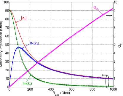
calculated them indirectly from other measurable parameters in the setup shown in Figs. 4.1 and 4.2. A straight forward set of measurable values could be the voltages across L1 and L2, which are named V1 and V2, respectively, when other variable parameters such as f, M, and RL are held constant. Obviously, V2 = VC1 - VC2 needs to be measured differentially in order not to disturb the transponder isolation from the reader.
To find the relationship between (V1, V2) and (Q2L, RLeq), we have further simplified the schematic diagram of Fig. 4.2 to the equivalent circuit model in Fig. 4.6. Here is how Q2L is defined,
eq L
L
C
R
Q
=
ω
2 , (4.4.1)2 2 2
R
L
Q
=
ω
(4.4.2)L L L
L
Q
Q
Q
Q
Q
Q
Q
+
=
=
2 2 2
2
||
(4.4.3)where, QL is the load Q-factor and Q2is the unloaded Q-factor of L2. It is also possible to find the voltage transfer function across the inductive link, FV = |V2(j
ω
)/V1(jω
)|, which derivation is given in the appendix, assuming QL2 >> 1 [23].We can write the KVL equations for the currents in L1 and L2, shown as I1 and I2, respectively.
)
(
)
(
)
(
, 2 2 1 2ω
ω
ω
ω
ω
j
Z
L
j
R
j
MI
j
j
I
eq L+
+
−
=
(4.4.4)) ( 1 ) ( ) ( 1 1 1 1 1
ω
ω
ω
ω
ω
j Z C j L j R j V j I R + + += (4.4.5)
where ZRis the reflected impedance on to the primary [23],
)
(
)
(
)
(
1 2ω
ω
ω
ω
j
I
j
MI
j
j
Z
R=
(4.4.6))
(
)
(
)
(
, 2 2 2ω
ω
ω
ω
j
Z
L
j
R
M
j
Z
eq L R+
+
=
⇒
(4.4.7)The secondary coil voltage is related to its current by,
)
(
)
(
)
(
2 ,2
j
ω
I
j
ω
Z
j
ω
V
=
−
×
L eq (4.4.8)Assuming QL2 >> 1 and that the primary and secondary tanks are often tuned at the carrier frequency, we can substitute (8) in (14) and reach at,
eq L eq L R
![Fig. 1.1. An implantable cardiac pacemaker device [1].](https://thumb-us.123doks.com/thumbv2/123dok_us/1739693.1222592/13.612.126.537.388.631/fig-implantable-cardiac-pacemaker-device.webp)
![Fig. 1.3. A state-of-the-art implanted deep brain stimulator [5].](https://thumb-us.123doks.com/thumbv2/123dok_us/1739693.1222592/15.612.206.450.70.334/fig-state-art-implanted-deep-brain-stimulator.webp)
![Fig. 2.2. (a) Neuron Model (b) Response of neuron to a stimulus [3]](https://thumb-us.123doks.com/thumbv2/123dok_us/1739693.1222592/21.612.145.489.69.617/fig-neuron-model-response-of-neuron-to-stimulus.webp)


![Fig. 4.8. The reflected impedance (ZR) at the primary shown in the complex plane as a function of equivalent loading at the secondary (RL,eq), with RL,eq ascending from left to right in the range 1 Ω – 1 kΩ [6]](https://thumb-us.123doks.com/thumbv2/123dok_us/1739693.1222592/65.612.126.529.71.373/reflected-impedance-primary-complex-function-equivalent-secondary-ascending.webp)