MICROPROCESSOR
BASED MULTIFUNCTION
SIGNAL GENERATOR
/(
By
1
KARIMI P. MW ANGI
A
THESIS SUBMITTED IN PARTIAL FULFILMENT FOR THE
DEGREE OF MASTER OF SCIENCE
KENYATTA UNIVERSITY
OCTOBER, 2001
Karimi, P.Mwangi
Microprocessor bassed multifunction signal
This Thesis is my original work and has at any other University.
Karimi P. Mwangi
___...•resented for the award of a degree..
(156/8441/98)
Department of Physics Kenyatta University P. O. Box 43844 Nairobi, KENYA
t1
J"
1
;
)
-
0
.
;)'
~
This Thesis has been submitted with our approval as University Supervisors.
Dr. G. A. Ibitola Department of Physics Kenyatta University P. O. Box 43844
Nairobi, KENYA
~
.
~Signature
/-\\-Ztmt
DateDr. R. L. Stangl Department of Physics Kenyatta University P. O. Box 43844
Nairobi, KENYA
9-11-~0Cri
DateDr. S. Namuye
Department of Computer Science Kenyatta University
III
DEDICATION
This work is dedicated to my parents
Karimi Munu and Beatrice Nyambura.
ACKNOWLEDGEMENTS
Let me take this opportunity to specifically thank all my lecturers in the department of physics, especially my supervisors Dr. G.A. Ibitola, Dr. R.L. Stangl and Dr. Sylvester
amuye, who guided me all through this research. 1 am also grateful to Kenyatta University for providing me with a full scholarship, which financed my studies.
Special thanks also go to Dr. Gakuru and the entire Department of Electrical Electronic Engineering (Nairobi University) staff for giving me consent to use their 8086 microprocessor kit, EPROM programmer and all other facilities intheir microprocessor laboratory without interference.
v
TABLE OF CONTENTS PAGE
DECLARATION 11
DEDICATION 11I
ACKNOWLEDGMENT IV
TABLE OF CONTENTS V
LIST OF TABLES IX
LIST OF FIGURES X
ABSTRACT XII
CHAPTER 1 1
INTRODUCTION 1
1.1 A General Overview I
1.2 Microprocessors 3
1.2.I Data Bus 4
1.2.2 Address Bus 4
1.2.3 Control Bus 5
1.2.4 Internal Registers 5
1.2.5 Clock System 5
1.2.6 Microprocessor Applications 6
1.2.78088 Microprocessor 7
1.3Computer Programming Languages 9
.1.3.1 Machine Language 9
1.3.3 High-Level Language 11
1.4 Main Memory Subsystem 12
1.5 Objectives 13
1.6 Rationale IJustification Of The Study 14
CHAPTER 2 16
LITERATURE REVIEW 16
2.1 Signal Generators 16
2.2 Analogue Signal Generators 17
2.3 Digital Signal Generators 19
CHAPTER 3 23
R£SEARCH METHODOLOGY 23
3.1 An Overview 23
3.2 Programming the erasable programmable read only memory (EPROM 2716) 26
3.3 Testing and Analysis 27
3.3.1 Technique No. 1 (Direct Testing Method) 27
3.3.2 Technique No. 2 (Indirect Testing Method) 28
CHAPTER 4 29
THE SYSTEM DESIGNS 29
4.1 The System Hardware Design 29
4.1.1 MBM Signal Generator Circuit Description, Operation and Construction. 29
vii
4.1.3 Reset 34
4.1.4 Memory 35
4.1.5 Programmable Peripheral Interface (8255A PPI) 38
4.1.6 Digital to Analogue Converter (DAC 0800) 39
4.3 The System Software Design : 40
4.4 Generation Of The Signal Waveform Bits 44
4.4.1 Sine Wave generation 44
4.4.2 Triangular Wave generation 45
4.4.3 Square Wave generation 46
4.3.4 Ramp Wave generation 47
4.5 Frequency Generation 54
CHAPTER 5 : 55
RESULTS AND ANALySIS 55
5.1 A Working System And Analysis Of Waveforms Generated 55
5.2 Analysis Of The Generated Frequencies 58
5.3 Spectral Analysis : 60
5.3.1 Square Wavefunction 60
5.3.2 Ramp 60
CHAI)TER 6 62
CONCLUSiONS 62
6.1 Summary and Recommendations 62
6.2 Suggestions for Further Work 62
REFERENCES 64
APPENDIX A 69
PROGRAM LISTING 69
APPENDIX B 80
8086/8088 INSTRUCTION SET 80
APPENDIX C 84
CARRYING OUT MEASUREMENT FROM MBM SIGNAL GENERATOR WITH THE PM 3384
AUTORANGING COMBJSCOPE 84
APPENDIX D 86
8088 MICROPROCESSOR PIN CONFIGURATION 86
APPENDIX E 87
PHOTOGRAPH OF THE MBM SIGNAL GENERATOR 87
APPENDIX F 88
IX
LIST OF TABLES
Table Page
Table Ll :8086/8088 Intel Processor Specifications 7
Table 4.1 Memory map nomenclature of the MBM signal generator. 37 Table 4.2: Symmetrical Offset Binary Operation Of The DAC. .40
Table 4.3: Software-Look up Table For Sine wave 47
Table 4.4: Software-Look up Table For Triangular wave .48
Table 4.5: Software Look -up Table For Square wave 50
Table 4.6: Software Look -up Table For Ramp 51
Table 4.7: Software Look -up Table For Staircase 52
Table 4.8: Software Look -up Table For Random wave 53
Table 4.9: Software generation of frequency of 1Hz 54
LIST OF FIGURES
Figure Page
Fig. I.1:The basic input- output signals associated with a microprocessor. .4 Fig.2.1: Block diagram of Analogue multifunction signal generator. 17 Fig.2.2: Analogue Circuit of multifunction Signal generator. 18 Fig.2.3: The basic block signal diagram of adigital signal generator. 19 Fig.2.4: The circuit diagram of digital signal generator. 20
Fig.3.!: Flow chart of the research methodology 24
Fig.3.2: Schematic diagram of system evaluation: Technique No. 1 28 Fig. 3.3: Schematic diagram of system evaluation: Technique No. 2 28
Fig. 4.1 Block diagram of MBM Signal generator. 3!
Fig. 4.2 Complete circuit diagram ofMBM Signal Generator. 32 Fig. 4.3: Block diagram of the clock generator circuit of the microprocessor
controlled signal generator. 33
Fig. 4.4: Block diagram of the reset circuit of the microprocessor
controlled signal generator. 34
Fig. 4.5: The decoder configuration 37
Fig. 4.6: Block diagram of the 8255A Pl'L. 38
Fig. 4.7: DAC 0800 wiring configuration .40
Fig. 4.8: Flow chart of the control software for the Microprocessor
Controlled Multifunction signal generator. 42
Fig. 4.9: sinusoidal wave 44
XI
Fig. 4.1 I: Square wave 46
Fig. 4.12: Ramp Waveform ··· 47
Fig. 5.1: Sine Waveform Generated by MBM Signal Generator. 55
Fig. 5.2: Square Waveform Generated by MBM Signal Generator. 55
Fig. 5.3: Triangu\ar Waveform Generated by MBM Signal Generator. 56
Fig. 5.4: Ramp Waveform Generated by MBM Signal Generator. 56 Fig. 5.5: Staircase Waveform Generated by MBM Signal Generator. 57
Fig. 5.6: Dispersion of the mean observed frequencies from the expected
ABSTRACT
Waveform generators are excellent tools to recreate real-world signals that offer precise sirnulations for innumerable challenging test conditions. Waveforms are, for example
used in airbag deployment, multi-tone amplifier testing, brake simulation, digital modulation, cardiac device calibration, power disturbance harmonic generation, laser beam control and wafer cleaning drive signals among many others. The possible waveforms that can be been generated include: Sine, Cosine, Triangle, Ramp, Exponential, Gaussian, Pulse, Sine, Hamming (Sine), Amplitude modulation (AM),
Frequency modulation (FM), Frequency shift keying (FSK), Phase shift keying (PSK), Noise-Digital, Noise-Analogue, Comb, Steps, Sweep, Cardiac and Squine.
Inthis research work, the generation of square, sine, triangular, and random waveforms using a microprocessor-based programmable waveform generator is presented. The 8088 microprocessor and other support chips, hardware and software designs are
discussed. Analysis and experimental results based upon the system and its associated
waveforms are evaluated using a PM 3384 autoranging combiscope (CRO). The function generator is a prototype of general-purpose, high performance instrument capable of generating standard waveform patterns at frequencies of exceptionally low distortion. The generator is capable of generating frequencies, selectable from 0 Hz to 100Hz and adjustable output amplitude from
±
4.8 V to±
14.1 V peak to peak with highresolution. The system as a whole possesses some interesting advantages over the analogue and digital types of signal generators that are presently in use.
CHAPTER 1
INTRODUCTION 1.1 A Ceneral Overview
This thesis is about the design, construction and testing/ calibration of a microprocessor-based multifunction signal generator (MBM signal generator). There are already in existence today analogue and digital signal generators, which however, have some undesirable limitations. The MBM signal generator is an improved version of the IC 555 timer- based digital signal generator and has several advantages over the currently used analogue and digital signal generators.
Waveform/function generators are excellent tools to recreate real signals and offer precise simulations for innumerable challenging test conditions. They are used in six different major categories [1]:
• Acoustic and audio
• Medical • Automotive
• Power
• Communication
• Semiconductor applications
bearing failure assessment, amplifier linearity testing and multi-tone response
eval uation.
In the medical field generators offer diverse applications such as threshold testing and monitor evaluation, patient display monitor testing and pacemaker certification among
others.
In automotive systems, function generators are used for airbag deployment, electronic security orders, ignition timing signals, suspension actuation and brake simulation.
The use of function generators in power includes simulating power disturbances to
activate distribution relays or circuit breakers (harmonic generation), precision phase
angle control, utility meter calibration and uninterruptible power supply testing.
In communication, applications include modem testing, radio data simulation,
modulator phase sensitivity measurements, pseudorandom code patterns and intermodulation distortions.
Waveform variety punctuates scientific areas of applications. Uses range from ultrasonic wafer cleaning, semiconductor device evaluation, laser beam control, to fluid flow metering.
3
digital signal generators lack control programs and are characterized by poor responses
in terms of settling times, phase shifts, amplitude and frequency [5, 6, 7]. As a microprocessor is at the heart of the MBM signal generator to be discussed in this work
abrief introduction into microprocessors is given in the following section.
1.2 Microprocessors
The microprocessor is a digital device able to receive information in the digital form,
process this information according to a stored program and output information in the
form of digital signals [8]. It acts as a control centre for all operations and executes instructions that are contained in the memory subsystem. The basic operations of the
microprocessor include:
• the transfer of data between itself and the memory section
• the manipulation of data in the memory subsystem
• the transfer of data between itself and input/output devices
In order to facilitate the transfer of data and instructions between the microprocessor,
memory and input/output devices, the following major buses (groups of lines or pins sharing an information) are used:
• Address bus
• Data bus, and
Control bus
< >
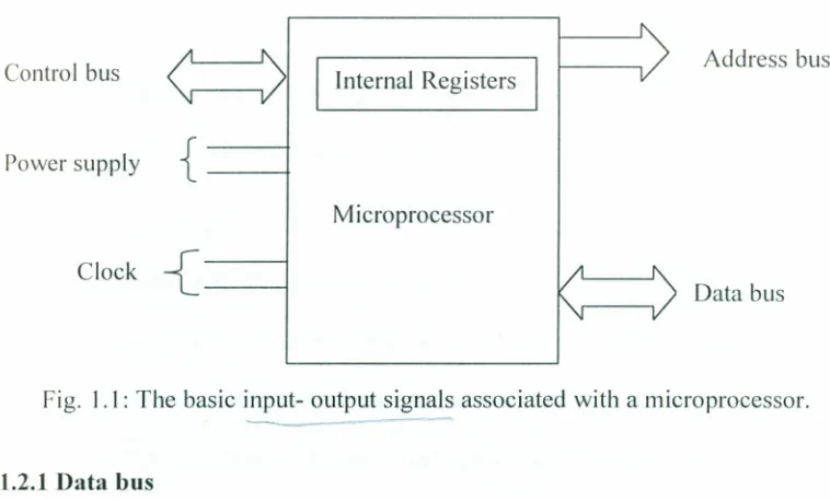
Address busInternal Registers
{
Power supply
Microprocessor
{
Clock
Data bus
Fig. 1.1: The basic input- output signals associated with a microprocessor.
----1.2.1 Data bus
Any transmission medium that has more than one outlet at each end is called a bus The processor data bus is a bundle of wires (or pins) used to send and receive digital
signals. The more signals that can be sent at the same time, the more data can be transmitted in a specified interval and, therefore, the faster the bus.
1.2.2 Address bus
The address bus is the set of wires that carry the addressing information used to identify the memory location to which the data is being sent, or from which data is being retrieved. As with the data bus, each wire in an address bus carries a single bit of information. This single bit is a binary digit in the address. The more the wires (digits)
5
1.2.3 Control bus
The control bus provides timing signals to synchronise the flow of data between the processor and memory subsystem or peripheral devices.
1.2.4 Internal registers
The size of the internal register is a good indication of how much information the processor can operate on one at a time. Most advanced processors today, from the 386 to the Pentium use 32-bit internal registers and 32- 64 bit data buses. Some processors have an internal data bus (made up of data paths and of storage units called registers) that is different from the external data bus. The 8088 and 386SX are examples of this structure. Each chip has an internal data bus twice the width of the external bus. These designs are called hybrid designs. The 386SX, for example, can pass data around internally with a full 32-bit register size. For communications with the outside world, however, the chi p is restricted to a 16-bit-wide data path. Internal registers often are larger than the data bus, and thus the chip requires two cycles to fill a register before the register can be operated on. The Pentium is an example of the opposite situation.
1.2.5 Clock System
system runs at millions of these cycles per second, so speed is measured in megahertz
(MHz) where one hertz is equal to one cycle per second.
In building a processor, a manufacturer tests it at different speeds, temperatures, and
pressures. After the processor is tested, it receives a stamp indicating the maximum safe
speed at which the unit will operate under wide variations of temperatures and pressures encountered in normal operations.
The size of the data and the address buses, the types of control signals in the control
bus, the power supply and clock requirements vary from one microprocessor to another In rcroprocessor.
1.2.6 Microprocessor Applications
Microprocessors are applied in three principal ranges of operation: Control, calculation
and administration [8, 9]. Many applications that previously employed hardwired logic have been made feasible by use of microprocessors. Specific applications range from
the retail shop price machines to sophisticated equipment like oscilloscopes, frequency synthesizers and TV games. In the process industry, microprocessors are now used for
implementing a number of process-control algorithms as economic alternatives to
conventional analogue controllers. They have the advantage of being programmable and hence more flexible. ln the automobile industry a few recent car models include
7
microprocessors ranging from 8086/8088 to Pentium III1IV processors (running at 1.5 GHz or more) are more suited to complex signal-processing applications [14].
The final level of microprocessor usage is the multiprocessor system where several
dedicated microprocessors are teamed to monitor and control a large industrial plant.
For example, the continuous casting of steel slabs uses a complex control system for maintaining temperature, valve pressure flow rate within prescribed limits, at successive stages, utilizing anumber of microprocessors [15,16].
In this research work, 8088 microprocessor is used for optimum control of the generation of the standard waveforms and other pre-stored waveforms.
1.2.7 8088 Microprocessor
The 8088 combines the powerful resources of a 16-bit rrucroprocessor internal
architecture with an easy to use 8-bit bus interface. The 16-bit internal architecture provides 16-bit wide registers, and allows the use of 16-bit instructions identical to the ones found in the 16- bit 8086 microprocessor. The 20-bit address bus of the 8088
-microprocessor allows it to access I Megabyte of memory as shown intable 1.1below.
Table 1.1: 8086/8088 Intel Processor Specifications
Processor Std. Internal Data- Address- Maximum Integral Integral Voltage Register Bus Bus Memory Cache Math
Size Width Width Co-processor
The data and address buses are independent, and chip designers can use whatever size they want for each. The sizes of the buses provide important information about a chip's relative power, measured in two important ways: the size of the data bus is an indication of the information-moving capability of the chip, and the size of the address bus tells
about how much memory the microprocessor can address.
The 8088 microprocessor has been used in this research project for the following reasons [17]:
• The 8088 microprocessor is 100% compatible with the 16-bit 8086 CPU, i.e. all the power of the 16-bit instruction set is available in the 8-bit 8088.
• The 8088 has a separate bus interface unit called the bus interface unit (BIU) whose job is to fetch instructions from memory and pass data to and from the execution
hardware to the outside world over the bus interface. Since the execution unit seldom needs to wait for the BIU to fetch the next instruction, there is less need for the BlU to fetch data quickly. Thus, the 8088 BIU allows maximum performance
and.processing power without high-speed memory devices in the system.
• The 5 MHz 8088 microprocessor can run at full speed using readily available Erasable Programmable Read Only Memories (EPROM's) with access time of
4S0ns whereas its counterparts, the 68B09 and Z80B, require wait states in their
9
The microprocessor is expected to process and output the data signals in digital forms.
The format and shape of the output signal from the 8088 microprocessor based
multifunction (MBM) signal generator will be governed by digital codes stored in the
EPROM memory units. The following microprocessor related parameters shall be taken
into consideration when using the 8088 MBM signal generator for optimal control of
the generator i.e. time constants, sampling rates, resolution and accuracy
[18, 19].
1.3 Computer Programming Languages
To run a program, a microprocessor must have the program codes stored in binary form
in successive memory locations. There are three language levels that can be used to
write a program for a microprocessor: machine language, assembly language and high
-level language [20].
1.3.1 Machine Language
This is a program written as sequence of the binary codes for the instructions that a
microcomputer is to execute. Small monitor programs allow the entry of these
instructions and data via hex keypads or terminals by the programmer. The
disadvantage of this method is that programs are hand-coded, which is a slow process
and also leads to translation errors e.g., the programmer could easily misread 8 as the
1.3.2 Assembly Language
Assembly language programming is done by writing machine instructions in mnemonic
form, using an assembler program to convert these mnemonics into actual processor
instruction codes and associated data. Mnemonics are symbols or the shortened form of
the English words for the operations to be performed by instructions.
Mnemonics are used because they:
-• are more meaningful than hex or binary values.
• reduce the chances of making an error.
• are easier to remember than bit values.
Assembly language statements are usually written III a standard form that has four
fields: Label field, Opcode field, Operand field and Comment field, e.g.
Label field
START:
Opcode field
MOY
Operand field
AX, OOH
Comment field
; clears the ax register
A label is a symbol or group of symbols used to represent an address which is not
specifically known at the time the statement is written. A colon usually follows labels.
Here, the label START is equal to the address of the instruction MOY AX ,OOH.
The opcode field (operation code) of the instruction contains the mnemonic for the
instruction to be performed.
The operand field of the statement contains the data, the memory address, the port
11
The comment field starts with a semicolon and is not part of the machine language
program. The comments in a program remind one of the function that an instruction
performs in the program.
The input program undergoes processing whereby the assembler reads the source program saved in the storage device (hard disk or a floppy disk). The assembler
program generates object code and list files as the output. The object file contains the machine codes for the instruction and information about the addresses of the instructions and is the one to be loaded into the memory for execution. The list file contains the assembly language statements, the binary codes for each instruction in
hexadecimal notation, the offset address for each instruction and it also indicates any
typing or syntax errors made in typing the source program. The advantages of an assembly language program are [21]:
• reduced errors
• faster translation times
• changes can be made easier and faster
The disadvantages of assembly language programming are:
• the programmer requires knowledge of the processor architecture and instruction set and thus any change in the hardware requires complete rewriting of the program.
1.3.3 High-Level Language
high-level language statements to machine codes, which can be loaded into memory and
executed.
Programs written in high level languages require more memory, execute more slowly
than the same programs written in assembly language program. Programs that involve a
lot of hardware control such as robots and factory control systems, that must run as
quickly as possible are usually written in assembly language program [22, 23].
However, complex data processing programs that manipulate massive amounts of data,
such as insurance company records are best written in a high- level language.
1.4 Main memory Subsystem
Memories are a combination of registers, each storing a multi-bit word (program or
data). Two distinct types of memories are used:
• Random Access Memory (RAM)
• Read Only Memory (ROM)
The information/data stored in RAM is lost when power is removed from it while that
of ROM is retained. RAM are of two types, Static RAM(SRAM) and dynamic
RAM(DRAM). DRAM requires periodic refreshing for maintaining the stored
information while SRAM does not, which is a major advantage of the former. When
program and/or data has to be stored and changed, static or dynamic RAM is used.
SRAMS are preferred when the memory size is not too large. For systems requiring
large memories DRAMS are used. The main reasons being of their high density, low
13
ROMs are of two types: masked-programmed ROM and User programmed ROM.
• Masked-programmed.
A masked-programmed ROM has the information written into it at the time of
manufacture.
• User-programmable ROM's are of two types:
-Programmable ROM (PROM) which can be programmed by the user once only by fusing the selected silicon links.
-Erasable programmable ROM (EPROM) which can be programmed, erased and
reprogrammed by the user a number of times.
Following is a list of features that are examined when selecting a specific memory chip
Capacity and organisations, Timing characteristics/ AC characteristics, Physical
dimensions and packaging, Cost, Reliability and Availability [24].
1.5Objectives
The general objective of this research project isto design and construct a microprocessor- based, programmable function generator required to generate:
(i) Sine wave,
(ii) Square wave,
(iii) Triangular wave,
(iv) Ramp wave, and
(v) Other pre-stored waveforms.
The use of the 8088 microprocessor for control of the generation of the waveforms is
(i) To have low distortion and stable signals;
(ii) To obtain high frequency stability;
(iii) To be flexible in waveform selection;
(iv) To have fast responses and automatic control; and
(v) To have storage facilities for useful signals.
1.6 Rationale / Justification Of The Study
Most scientific experiments, electronic testing, fault finding and process control systems
require stable, accurate and reliable signals. Therefore quicker, reliable, stable and more
accurate signal generation can be offered via the use of microprocessors as controllers
as attempted inthis research work. A microprocessor otfers greater flexibility, since bits
in memories replace wired connections. Thus, any modification in the hardware design
to improve signal generation is replaceable simply by reprogramming the system.
The project undertaken is to produce a prototype that demonstrates the effectiveness of
the programmable generator. This work has utilised the numerous advantages of
microprocessor-based systems to overcome the shortcomings inherent in the
generations of signals such as instability, distortion and slow responses. The sine,
triangular and square waves generated can be used for experimental work in the
University and College laboratory settings. The square wave that is generated can also
15
/ 1.7Thesis Organisation
This thesis is organised as follows:
Chapter 2 is a literature review that describes the history, development, advantages
limitations of various types of signal generators, and the improvements that would be
made. Chapter 3 presents a brief description of the research methodology adopted in
carrying out this work. In chapter 4, the hardware and software designs and construction
of the MBM signal generator js described in detail. The test/calibration results and
analysis of the MBM signal generator are presented in chapter 5. Chapter 6 gives the
CHAPTER 2
LITERA TURE REVIEW
2.1 Signal Generators
Research has been conducted on using rrncroprocessors in control and processing by
many reseachers. McOwitti A [25] designed and fabricated a measurement system
usmg Z80 microprocessor for maximum power measurement of a voltaic source
utilizing a resistor load . Owade M. [26] designed and developed a programmable
laboratory interface system with an illustrative use in resistivity temperature
measurement usmg Intel 8085 microprocessor. Research on rrucroprocessor
applications and feasibility of using microprocessors in industrial ancl process control
has also been widely done [27,28,29]. In this work, the 8088 microprocessor is used in
the control of the generation of standard and random waveforms (signals).
The signals that are usually generated have various wave shapes, which may be a sine
wave, a square-wave, or a triangular wave [30, 31,32,33].
The amplitudes (Vpk) of signals from signal generators usually range from 0 V to ± 10V, whilst their frequencies range from 0 Hz to 2 MHz [34].
Considering the foregoing discussion, a literature review on analogue and digital signal
generators is presented in the following sections, after which the attractive features and
16
CHAPTER 2
LITERATURE REVIEW
2.1 Signal Generators
Research has been conducted on using microprocessors in control and processing by
many reseachers. McOwitti A [25] designed and fabricated a measurement system
usrng Z80 microprocessor for maximum power measurement of a voltaic source
utilizing a resistor load . Owade M. [26] designed and developed a programmable
laboratory interface system with an illustrative use in resistivity temperature
measurement usmg Intel 8085 microprocessor. Research on microprocessor
applications and feasibility of using microprocessors in industrial and process control
has also been widely done [27,28,29]. In this work, the 8088 microprocessor is used in the control of the generation of standard and random waveforms (signals).
The signals that are usually generated have various wave shapes, which may be a sine wave, a square-wave, or a triangular wave [30, 31, 32, 33].
The amplitudes (Vpk) of signals from signal generators usually range from 0 V to
±
IOV, whilst their frequencies range from 0 Hz to 2 MHz [34].
Considering the foregoing discussion, a literature review on analogue and digital signal
generators is presented in the following sections, after which the attractive features and
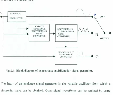
2.2 Analogue Signal Generators
Fig. 2.1 illustrates the basic system block design of an analogue signal generator, while
the associated real circuit which generates sine, square, and triangular waveforms is
presented in Fig. 2.2 [35].
±vs VARIABLE
(
\
)
.
.
--OSCILLATOR
-I
~ SCHMITT TRIGGERORMA
•.. RECTANGULAR
RECTANGULAR TO TRIANGULAR
-•.. WAVE ~ WAVE
-•..
CONVERTER CONVERTER
~
TRIANGULAR TO
.
ri
PULSESIGNAL
CONVERTER
•
Fig.2.1: Block diagram of an analogue multifunction signal generator.
\
B
e
---
e
OUTPUT
c
The heart of an analogue signal generator is the variable oscillator from which a
sinusoidal wave can be obtained. Other signal waveforms can be realized by using
suitable waveform converters. When the function select switch (SWF) is set at position
A, a sinusoidal wave is obtained. When SWF is set at position B, a triangular wave is
obtained at the output. SWF, being set at position C, yields a square wave or pulse
18
4Bk
IOk
Trla.""g\.oll
a,.-lOOk So---<J
Output
200k
Fig.2.2: Analogue Circuit of multifunction Signal generator
Analogue signal generators have been observed to possess the following drawbacks:
high cost, low accuracy, lack of memory- save- recall facility, low noise immunity, low
quality, low precision, and low signal resolution [36].
2.3 Digital Signal Generators
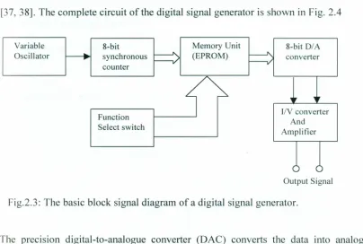
Fig. 2.3 shows the basic system block design of a digital multifunction signal generator
[37,38]. The complete circuit of the digital signal generator is shown in Fig. 2.4
Variable 8-bit Memory Unit 8-bit OfA Oscillator
--.
synchronous A (EPROM) ~ convertercounter
-v
r---v
0
r rIIV converter Function
And Select switch
Amplifier
Output Signal
Fig.2.3: The basic block signal diagram of a digital signal generator.
The precision digital-to-analogue converter (DAC) converts the data into analogue
voltage values. This series of sequential voltage levels describes the output waveform
with the frequency determined by the sample clock rate divided by the number of
samples in the waveform. Changing the sample clock rate from the 555 timer, achieved
by varying the lOOk linear potentiometer (Fig. 2.4), causes the address generator to
change the speed at which the data is presented to the DAC and thereby changing the
20
74163 counter cascaded to another 4-bit 74193 counter. The 8-bit counter produces the output from 00 to FFH, totalling 256 states, which stand as the lower 8- bits of the EPROM. The upper three bits include one that selects the desired functions, and one that changes the page of the EPROM.
When the output of the first counter becomes I Ill, the carry is produced which is given
to the count-up pin 5 of 74193. After the carry is produced, the first counter is reset and
it again starts counting from zero.
The waveforms created are a series of data points consisting of x- and y-axis values. In
describing the first point, 0 is given ay value. The next point has another y and so on, through the last address in the waveform .
I lOO.
, QI
01 .7
..fL----L.j"
IIC "
••1-"----...,
74193••
.
",} Function select switches
,--
-
---,
These series of points make the wave shape, which can be stored in large waveform
memories typical of digital generators. All the data points in the specified waveform
memory locations make up one waveform cycle. The waveform generator will output
all the points in the waveform at the sample clock rate specified. The resulting
frequency is equal to the sample clock rate divided by the number of data points inthe
waveform. If multiple cycles of the waveforms are entered into the same waveform
memory location, the output frequency will increase proportional to the number of
cycles in memory. The waveform frequency Fwis given by:
Where Fs
=
Sample clock rate (Hz)L
=
Waveform pointsN
=
Numberof data points in the waveform (2.1)The advantages of the digital signal generator are given as follows [39]:
•
high quality signals•
high output stability•
strong noise immunity•
high precision•
high resolution and22
However, the demerits ofthe digital signal generator are [40]:
• lack of logic control circuitry
• lack of control programs
• poor responses in terms of settling time, phase shifts, amplitude and frequency.
The following improvements were to be made on the digital signal generator so as to
obtain a microprocessor based signal generator:
(i) Provision of an expanded erasable programmable read-only-memory (EPROM)
for greater signal storage.
(ii) Provision of a wide range of frequencies based on the Microprocessors
capability.
CHAPTER 3
RESEARCH METHODOLOGY
3.1 An Overview
The methodology adopted in this research work is illustrated by means of a flow chart
given in Fig. 3.1. The appropriate hardware components for the system design were
selected on the basis of the following factors:
• operating temperature
• frequency response
• current rating and
• voltage rating.
The hardware components include: the 8088 CPU, 14.31818 MHz crystal oscillator,
8284A clock generator, 2.2/-lF capacitor, 10KQ resistor, 74LS373 latch, 74LS138
decoder, 7404 quad inverter chip, two 2716 (4K) EPROM, 6116 2K RAM, 8255A
programmable peripheral interface, DAC 0800 (digital to analogue converter), 741
operational amplifier, selector switches, reset switch and 10KQ potentiometer. The
circuit designed was simulated using the Electronic Workbench software. Thereafter,
the hardware design circuit was implemented and analysed for performance. The design
and implementation of the software involved the problem analysis, program design,
program coding, assembling, testing and debugging and documentation [41]. To
integrate the system software with the system hardware the program was burnt into the
24
START
PROBLEM DEFINITION
LITERATURE SURVEY
LITERATURE REVIEW
IDENTIFICATION AND STATEMENT OF THE
SYSTEM REQUIREMENTS/SP~CIFJCA TIONS
CIRCUIT SIMULATION/DESIGN
Cl RCUIT IMPLEMENTA TION
INTEGRA TING THE SYSTEM HARDWARE WITH SOFTWARE
NO TESTING AND ANALYSIS
RESULTS
O-K'!
ERROR DEBUGGING
AND REMOVAL
RECOMMENDA nONS
REPORT WRITING AND PRESENTATION
CEND~
Fig.3.1: Flow chart of the research methodology
In the problem analysis, the requirements of the program were clearly defined. This included defining of the segment registers to be used, port addresses of the
programmable input/output port and the memory map nomenclature. Program coding was done with an editor and given WAVEF.ASM file name after which the program
was assembled using 8086/8088-microprocessor Microsoft assembler version 5.1. which was performed as shown below [42].
• The correct path of the Microsoft assembler (MASM) was entered into the Microsoft disk operating system as follows:
C:\8086>MASM 4,..---"
Microsoft (R) Macro Assembler Version 5.10
Copyright (C) Microsoft Corp 1981,1988. All right reserved
Source filename [.ASM]: WAVEF
Object filename [C: WAVEF.OBJ]: Source listing [NULL.LST]: WAVEF Cross reference [NUL.CRF]:
47696
+
364363 Bytes symbol space freeo
Warning Errorso
Severe Errors C:\8086>The assembled program WAVEF3.0BJ was then converted into a uitable format (Intel
26
C:\8086>LOD 186 ••_---l
Paragon LOD186 Loader- Version 4.0h
Copyright CC)1983-1986 Micro-tech Research Inc.
ALL RIGHTS RESERVED.
Object/Command File
Output Object File
Map Filename
**LOAD COMPLETE
[.OBJ]:WAVEF 4.--'
[C: WA VEF.ABS]: ••_---l
[C:NULL.MAP]: 4.----l
3.2Programming the erasable programmable read only memory (EPROM 2716)
The WAVEF.ABS file was loaded into the erasable programmable read only memory
(EPROM 2716) with the help of EPROM programmer Omnipro2 as follows [43].
• The pins were checked for proper contact with the socket in the Omnipro2 EPROM
programmer.
• The EPROM was checked whether it was inserted in the correct orientation in the
Omni-pro2 EPROM programmer.
• The EPROM was then checked whether it was blank/erased. A blank EPROM has
all its bits set to logical l(i.e. the content of all the memory locations are FFH).
After a blank check failure, the EPROM was erased using EPROM eraser, which
• After the success of the above check, the appropriate address of the random access
memory (RAM) of Omnipro Il corresponding to the physical address of the
fabricated hardware of the 8088 microprocessor controlled signal generator was
given and data (WA VEF.ABS file) written to it from the personal computer.
• The EPROM was then brought in the program mode and all the data stored in the
RAM locations were transferred inthe EPROM.
• After the chip was programmed, it was brought in the verify mode whereby all the
programmed contents in the EPROM were compared with the RAM contents. The
verify signal was displayed if the comparison was correct.
The program was then integrated with the hardware for purpose of testing. The
troubleshooting of the hardware was carried with the help of logic probe, logic pulsars
and cathode ray oscilloscope. The software errors encountered during testing were
debugged and the whole process repeated until it was ascertained that the program was
free from errors. The final program was integrated with the hardware and the whole
ystem tested and analysed for overall performance.
3.3Testing and Analysis
The integrated system was evaluated using the following procedures.
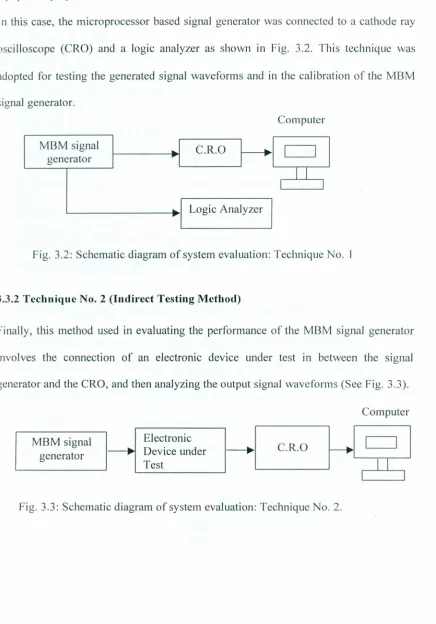
3.3.1Technique o. 1(Direct Testing Method)
This method of testing and analyzing the output signals of the MBM signal generator
28
generator and the test equipment but analyzed by connecting it directly to the test equipment [44].
In this case, the microprocessor based signal generator was connected to a cathode ray
oscilloscope (CRO) and a logic analyzer as shown in Fig. 3.2. This technique was
adopted for testing the generated signal waveforms and in the calibration of the MBM signal generator.
Computer
MBM signal C.R.O
I
•..generator
I
•..•.. Logic Analyzer
•..
Fig. 3.2: Schematic diagram of system evaluation: Technique No. I
3.3.2 Technique No. 2 (Indirect Testing Method)
Finally, this method used in evaluating the performance of the MBM signal generator involves the connection of an electronic device under test in between the signal generator and the CRO, and then analyzing the output signal waveforms (See Fig. 3.3).
Computer
MBM signal •.. Electronic Device under generator
•
..
Test
CHAPTER 4
THE SYSTEM DESIGNS
The system design consists of two parts, namely: the hardware and the software
designs. This chapter describes the various components of the two designs, their
operation and performance.
4.1 The System Hardware Design
The MPU 8088 based signal generator: consists of the 8088 microprocessor, clock
generator circuit, main memory (two EPROM 2716 chips and one RAM 6116 AP chip),
decoder circuit, address latch (74LS373), programmable peripheral interface (8255A),
selector switches, digital to analogue converter (0800 DAC) and current to voltage
converter (741 operational amplifier).
4.1.1 MBM Signal Generator Circuit Description, Operation and Construction
The system block diagram of the MBM signal generator is illustrated in Fig. 4.1. On
powering up the system the reset circuit initialises the system after which the wave
generation software is loaded from the memory subsystem (EPROM No.1 and EPROM
No.2). Whether the memory subsystem or input/output chip (8255A) is being accessed
is determined by rO/M signal from the 8088 microprocessor. This pin is connected
directly to the decoder (74LS 138) for memory selection and is connected to 8255A
programmable peripheral interface active low chip-enable pin through a NOT gate for
30
signal, which depends on the decoding circuitry (74LS 138 decoder). The 8255A chip has its ports configured as follows:
Port A as input port for waveform selection, Port B as an output port for outputting the digital word corresponding to desired wave function and port C as an input port for frequency selection. The digital-to-analogue converter (DAC 0800) converts the digital signal from port B of the 8255A PPI to acorresponding analogue signal equivalent. The current output from the DAC 0800 is then applied to a current-to-voltage converter (OPAMP 741) and the peak-to-peak amplitude of the analogue signal is obtained or adjusted by means of a 10 KO potentiometer. The final analogue output signal is then
fed into a CRO for display and analysis.
c
,---
--=nvet
"---j<~jOT (
-
.
\ /
~---~
'" ~Uital Output (Port B)
ter
gnte)j
-
----
~
DAC (0800)
171
/ Ar:plitu de Adjustr'1ent Port
,,!/
--I1V
Convert-er'&.
Anpllf l
er-6
Analogue output
74lS04
Vcc
.---~-
__
1{>~----A19/S~3~5~---~---.---' A18/Ss->3!.>!6,--_
At71S-4i-=3:.:.7 __
A16/S~3~9,--_
At5 39 At4
1-';:1"'----At31-'3"'-- _
At2~4L-
---Atl
~~L
-
---
__---Ato~~~---~
~ ~7~---
__---~7~:t=~====~m===~~====
AD6r'~n~~---~~AD5r~11.-~~ ~
AD4 '"
AD3 ,~
AD2r~"4~~r+;-~--~
ADl 1~
ADor~16~~r+~r+~~
~~ '---__ ~2BID/M
t
-
---
.
...,
•
.
·RESET.
Vcc
.
..~~b~J
L
(t-- - l6 X2re
I~~ "~~ m
~ ~YNC ~ RSTI-'=-II---'
f
---
f
-
fIe ClKt-=-8---.O.L.j19ClK':=±
A£N2 RDY s 22 READY~ 11
----L CSYNC j--=-4 Vcc
OSC~
PCK~
8088
t---37:3;-;MN/MX
40
.-_--,2,O...,GND
t---~2:-.!'-13~
t---~l;'t18~~1R r--~"'"'"-iHOlD
FIg.4,21The COl'lplete Circuit DIa.gro,l'I Of the MCM Slgna.l Genera.tor,
Vee GND'
--"'
19 9Q 19
17
7D 7Q 16
146D 6Q 15
-5D 5Q,~~ 9 4D ~-..j 4Q
r 7 3D
"" 3QI6
w
4 2D -w..j 2Q~ 3 1D
i6
I~
VCC EN Jll I -'L- _
74LS04
-""-
--.--h
-
-
-
~~~---
v~
r---,~ Vc:c:
-5. G2B
4 G2A
Vc:c:--t 6 -..j GND~ .~
r en •... w CD ~C :> B
L---. I A
..-r
"---BQ&...
A7
7 16
.
AA6 15
-
3 It:J~
11"
.
.
A45QI9
s
A3
~
4Q, ~
3Qj6 6 AI. li\
2Q~ 7 AI
lQ"[2
•
All '[10I
-.
C"-~J
r-, -l -• A7 • AA 101 MI AS ". A4 Ir
·
A3 oWl• AI! N aa.
--L. AI -•....j. 117
.-.-L All C1\ D6
11:I D4 D3
.
~
112m
-• A7-;-:
A4 • A3 • AI!U:
-.
C"-'-- ...J
1---. DO
DI
p--.
Da
-
lI204
D:I
1---.
-116
1---,
Il7
~
i
+12Vr1
i1I1Z1IIU!l1 1. • 4 I ,-_. DAC0800;;:1. •C
74-==-...-
-
'., ~
7=
jti~~
/.
IGIC -12V+ZV -12V
To CAllrer 1JIIPa,
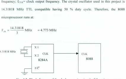
4.1.2 8284A Clock Generator
The 8088 requires a clock signal with fast rise and fall times (IOns maximum) between low and high voltages. This is provided by lntel 8284A clock generator and driver. This generator supplies a train of pulses at a constant frequency and synchronizes ready
signals, which indicate an interface is ready to complete a transfer and reset signals which initialises the system, with the clock pulses. The frequency source applied to the
8284A may be from a pulse generator that is connected to the external frequency input
pin (EFL pin) or an oscillator that is connected across XI and X2. If the input to frequency/ crystal select input pin (F/e) is 1, then the EFT input determines the frequency; otherwise it is the oscillator input. In either case, the clock output eLK, is one third of the input frequency (fe=3 x fCLK); where
f
,
isthe crystal or pulse generator frequency; fCLK= clock output frequency. The crystal oscillator used in this project is14.31818 MHz TTL compatible having 50 % duty cycle. Therefore, the 8088
microprocessor runs at:
F =14.31818MH
clk 3 . z = 4.773 MHz
Fie
X2 CLK
8284A
CLK
8088
X 1
14.31818 MHz
c::J
34
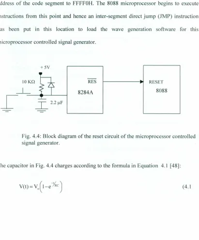
4.1.3 Reset
Reset is for inputting a system-reset pulse. A switch that allows the operator to
reinitialize the system manually generates the reset pulse in this system. The 8088
require an active high reset after which the components go to their "turn on" state. For
this microprocessor, this turn on state clears the flags, Queue, instruction pointer, data
segment register, stack segment register, extra segment register and sets the physical
address of the code segment to FFFFOH. The 8088 microprocessor begins to execute
instructions from this point and hence an inter-segment direct jump (JMP) instruction
has been put in this location to load the wave generation software for this
microprocessor controlled signal generator.
lOKQ RES
+5V
RESET
8088
_
1
-I
--e----'----
1
-
I
2.2 flF8284A
Fig. 4.4: Block diagram of the reset circuit of the microprocessor controlled signal generator.
The capacitor in Fig. 4.4 charges according to the formula in Equation 4.1 [48]:
From the A.c. characteristics of the 8088 microprocessor VLOW(max)= 0.8 V and time it takes the microprocessor to read the RESET input after power up = 50 us. Substituting
for these values in equation 4.1, we get:
(4.2)
From which the minimum time constant required is
1:=0.28ms (4.3)
which could then be chosen from this value upwards such that Vet) approaches zero.
Assuming a capacitance of 2.2 ~F, the minimum resistance would be 128 O. It is therefore clear that the choice of R (lOKO) and C (2.2 ~F) gives a time constant which
i well above the minimum required time constant.
4.1.4 Memory
The memory used in this system includes two 2K x 8EPROM [Cs and 2K x 8RAM lC
whose details are given below.
a) Random Access Memory (RAM 6116 AP)
The RAM 61 16AP isa static read/write memory a low type complementary metal oxide
emiconductor organised as 2048 words x ~ bits with access time 120ns and voltage
36
The read enable RD and the write enable WE signals from the microprocessor are
directly connected to the 6116 AP RAM to enable read and write operations respectively.
The RAM used in this system is for stack operations and therefore stack segment is mapped onto it.
b) Erasable Programmable Read OnlyMemory (EPROM 2716)
The 2716 EPROM, 2048 memory locations erasable programmable read only memory used in this project, is an example of metal oxide semiconductor with access time of 450ns. EPROM 2716 is designed to work with microprocessor buses. Address lines (Aa - A10) of the EPROM are connected to the demultiplexed address bus (Aa - Ala) of
the 8088 microprocessor. The time multiplexed address bus/data bus (Aa - A7) of the
8088 microprocessor is connected to the data output of the EPROM. The 8088 read control line drives the output enable OE of the 2716 and enables the output data onto
the data bus from it with the proper timing to prevent bus contention problem. Generally, the It-bit address is submitted to an address decoding circuitry and a data word from the cell array is delivered at the data output pins. Because no on chip fuse destruction takes place, there is little risk of damaging the silicon by applying bad programming signals.
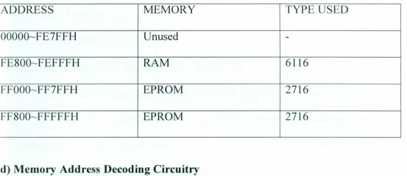
c)Memory Map
FFOOOH-FF7FFH and the second one mapped from location FF800H-FFFFFH. The
RAM IC used (6116 AP) hasbeen mapped to location FE800H-FE7FFH (see Table 4.1
for memory map nomenclature).
Table 4.1 Memory map nomenclature ofthe MBM signal generator.
ADDRESS MEMORY TYPE USED
00000-FE7FFH Unused
-FE800-FEFFFH RAM 6116
FFOOO-FF7FFH EPROM 2716
FF800-FFFFFH EPROM 2716
d) Memory Address Decoding Circuitry
The chip select CS inputs of the RAM and EPROM are driven by the transistor
-transistor logic (TTL) decoder (74LS 138) which maps the RAM 6116AP to FE800H
-FEFFFH memory locations. It maps the two EPROMs to address space (FFOOOH
-FFFFFH) addressable by the 8088 microprocessor. The chip select lines of RAM and EPROMs, driven bythe decoder, are brought to logic 0 when either of them is selected
by the microprocessor. See Fig. 4.5.
-
-[O/M G2B
-A[9/S6 G2A
8088
1
-
C 74LS138 3 •..CPU
•..
Decoder 2
•.
.
All B
•..
1
An A ~
EPROM
EPROM I
RAM
38
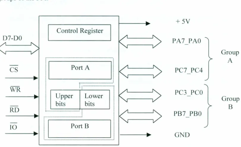
4.1.5 Programmable Peripheral Interface (8255A PPI)
Intel's 8255A is a programmable peripheral interface fabricated usmg MOS
technology and is contained in a 40-pin dual inline package. It is a parallel interface
where data/bits (D7_DO) can simultaneously be transferred over separate lines. 8255A
PPI contains a control register and three separately 8-bit addressable input/output ports.
The ports are labeled A, Band C. Whether or not an 8255A is being accessed is
determined by the signal on the CS pin and the direction of access is according to the
read RD and write WR signals. The bits in the three ports are attached to the pins that
may be connected to the input/output device. These bits are divided into groups A and
B, with group A consisting of bits in port A (PA7_PAO) and the four most significant
bits (MSBs) of port C (PC7_PC4) and group B consisting of port B (PB7_PBO) and the
four least significant bits (LSBs) of port C (PC3_PCO). Figure 4.6 gives the various
groups of the PP!.
07-00
CS
RD
10
Control Register
I
I
Port A
I
Upper Lower bits bits
:
I
Port B
I
In this research project, the 8255A has been used in mode 0, a basic input/output mode
in which ports A and B can be individually configured as input or output, port C upper
or lower bits can also be individually configured as input or output. Therefore port A
has been configured as an input port for waveform selection, port B as an output port
for outputting the waveform digital codes and port C as an input port for frequency
selection. To achieve this, 10011001B(99H) is written on to the control register of the
8255A by the control program (See appendix A).
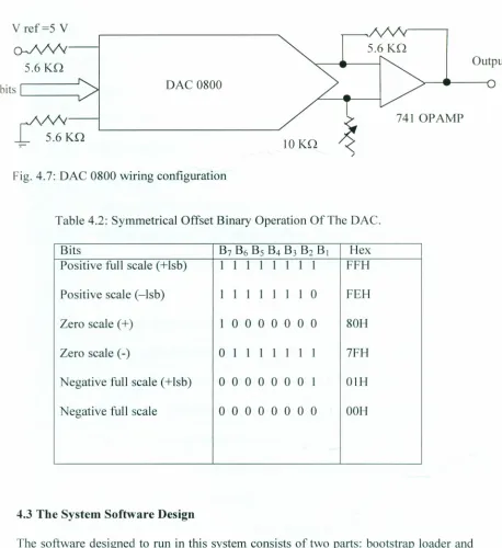
4.1.6 Digital toAnalogue Converter (DAC 0800)
The DAC 0800 is a monolithic 8-bit high-speed current output digital-to-analog
converter (DAC) featuring typical settling times of lOOns, full scale error of ± Isb, non
linearity over temperature ± 0.1%, high output compliance =l Ov to
+
18Y, wide powersupply range ±4.5 to 18Y, complementary current outputs and interfaces directly with
transistor transistor logic and complementary metal oxide semiconductor. The DAC
0800 also features high compliance complementary current outputs to allow differential
output voltage 0[20 Ypp with simple resistor loads.
Each function is stored in the EPROM in the form of particular digital codes (B7 BO),
see table 4.2. When the complete address is available to the EPROM from the 8088
microprocessor and the selector switches, it produces the particular function in the
digital output. This DAC is used to convert the digital codes into analogue form that can
be displayed in the PM 3384a-autoranging combiscope. The DAC was wired as shown
V ref=5 V
o
-
ANY-5.6KO
40
ANY---.
5.6 KO
8bitsL- __ ----, DAC 0800
ANY
I
5.6 KO10KO
Fig. 4.7: DAC 0800 wiring configuration
Table 4.2: Symmetrical Offset Binary Operation Of The DAC.
Output
7410PAMP
Bits
Positive full scale (+Isb)
Positive scale (-Isb)
Zero scale (+)
Zero scale (-)
Negative full scale (+Isb)
Negative full scale
4.3 The System Software Design
Hex
The software designed to run in this system consists of two parts: bootstrap loader and
11111111 FFH
I 1 1 1 1 1 1 0 FEH
1 000 0 0 0 0 80H
01111111 7FH
o
0 0 0 0 0 0 I 01Ho
0 0 0 0 0 0 0 OOHthe system control software (waveform generation software).
(a) Bootstrap loader: the bootstrap loader initialises the code segment to start at
memory location FFOOOH (the first memory location of the cascaded EPROMs)
(b) Waveform generation software: consists of several subroutines, which are to be
called sequentially as required for execution. The main system software consists of the
following subroutines:
(i) INIT: This subroutine initialises segment registers, programmable port
devices and the stack pointer. The data segment was initialised to start
at memory location FFOOOH and the stack segment to start at the first
memory location of the RAM (FE800H) with stack pointer loaded with
100H as an offset to the stack segment. The binary number 10011001
was loaded to the 8255A PPI control register to configure the ports as
follows:
Port A as input port for waveform selection, Port B as output port for
outputting the selected digital codes for the different wave-functions and
port C as an input port for selecting the desired frequency.
(ii) POLL: This subroutine selects the desired waveform out of the six to
give the appropriate signal function.
(iii) DELAY 1: This subroutine selects the desired signal frequency out of
the eight different frequencies.
Algorithms for system software for the above modules (see Fig. 4.8) have been
developed and coded in 8086/8088-assembler language and the control program listing
YES Read up thetriangular
-
0
wave bits from the
lookup table
POLL
YES Read up the ramp wave
-()
bits from the lookup
table
C
BEGIN ~t
CRESET~
Initialise The Segment Registers (Code
INIT Segment, Stack Segment, Data Segmen
and Extra Segment
Load the necessary
Control byte from port A
to the accumulator
Read up the sine wave
(0
bits from the lookup ---. A
table
NO
Read up the square wave bits from the
lookup table
Read upthe staircase
wave bits from the
lookup table
Read up the random
8
wave bits from the ---. Flookup table
'----_---J
Fig. 4.8: Flow chart ofthe control software for the Microprocessor Controlled
0
---
+
1
L---r---~
Transmit the signal bits to th
r-
:
\
output port B ofthe 8255A PPII
"
'~'
-
-
-V
Enable the DAC for conversion
DELAY}
Tune to the correct frequenc
(input the control bits to port C0 the 8255A PPI to call th appropriate delay routine)
Adjust the Analogue Signals
Amplitude as desired
Output the desired signal to the output Device (CRO)
END
Fig. 4.8 (CONTD.): Flow chart of the control software for the Microprocessor
44
4.4 Generation Of The Signal Waveform Bits
4.4.1 Sine Wave generation
The look-up table is obtained through an analysis, which IS described as follows.
Considering a typical sinusoidal wave as shown in Figure 4.9
v 5 nu so o'o t wo.ve
80H
FFH
OOH
-
I
Fig. 4.9: sinusoidal wave
The maximum value according the DAC 0800 is FFH and the minimum value is OOH.
The zero (reference) level is 80H and the amplitude is 128 units above the zero
reference level. Since the signal bits are stored in 256 memory locations then the angle
corresponding to each memory location is given by:
n
8=-x360 256
Where n= 0,1,2 ..256
The maximum amplitude is obtained at 8= 90° which from inspection is 1 and
corresponds to an amplitude of 128 units above the zero reference level according to the
configuration of the digital to analogue converter. Therefore each digital word
sin(~ x360) x 128 units in Hex form
+
80H256
for 0 ~ n~ 128 and
80H - sin(~ x 360J x 128 units in binary form 256
for 128 ~ n~ 256
For example, when n=l, sin
e
= 0.02450 and the decimal equivalent is 0.0245° x 128 =3.136 which after rounding off equals to 3.0.
The hexadecimal equivalent of3.0 is 03H. Since the reference point is 80H, the value to be stored in the EPROM is 03H
+
80H = 83H. The digital equivalent for the otherangles were determined in the same way and stored in the look-up Table 4.3
4.4.2 Triangular Wave generation
The triangular wave (Figure 4.10) is represented by the functions below:
2
Y =-t,
1t
2
2
y = - - t
+
c, y= - t - c Where c is a constant.1t 1t
FF1--I
v
I
-rr o.ngulo.r wo.veV\
/\!\
7FH
t
OOH
46
The amplitude is 128 units above the reference level that corresponds to ~ rad 2 The general formula for determining the amplitudes is
amplitudes
=
2
.
x2n where n=
0,1,2 .. 256256
which after conversion into units above the reference level is given by 2n
The byte to be stored in the EPROM is then determined by:
2n (in Hex format)
+
7FH for 0:s;n :s; 128,FFH - 2n (in Hex format) for 128 :s;n:s; 192 and
OOH- 2n (in Hex format) for 192 :s;n:s;256
after which look-up Table 4.4 was prepared.
4.4.3 Square Wave generation
y
=
A, y=
-A where Aand - A representsFFH and OOH(the amplitudes of the square wave signal) respectively.
which is illustrated in Figure 4.11. The bytes stored in the EPROM to realise one cycle of the square wave were FFH for the first 128 memory locations and OOH for the next
128 memory locations (see look-up Table 4.5).
v]
FFHC
7FH
OOH
I
pvlse/squQre WQve
I
27t t
4.3.4 Ramp Wave generation
The ramp waveform was realized from the formula y
=
~n t (Fig. 4.12) 2FFH
7FH
2n
Fig. 4.12: Ramp Waveform
The general formula for determining the amplitudes is:
amplitudes (in rad) = ~ x2n where n=0, 1,2 .. 256 256
The general formula for determining the amplitudes in decimal is:
Amplitude in decimal
= ~
and hence the value to be stored in the EPROM is2
~ (in Hex)
+
7FH, where n=
0,1,2 ..256 2For example:
For n=1,the byte to be stored in the EPROM is 01 H
+
7FH =80H (see look-up Table 4.6)Along with the above waveforms, the look-up Tables for staircase and random
waveforms were prepared and the digital codes stored in the EPROM, look-up Tables
48
Table 4.3: Software-Look up Table For Sine wave
Memory Hex Memory Hex Memory I-lex Memory lIex Memory lIex Address code Address code Address code Address code Address code
0000 80 0034 1'13 0068 C6 009C 2D 00DO OB
0001 83 0035 FC 0069 C3 009D 213 OODI OC
0002 86 0036 FC 006A Cl 009E 29 00D2 OD
0003 89 0037 I'D 00613 BE 0091' 26 00D3 OF
0004 8D 0038 FE 006C BB OOAO 24 00D4 10
0005 90 0039 FE 006D 138 OOAI 22 00D5 11
0006 93 003A 1'1' 006E 135 00A2 20 00D6 14 0007 96 00313 1'10 0061' 133 00A3 lE 00D7 15
0008 99 003C 1'1' 0070 Ba 00A4 IC 00D8 17
0009 9C 003D 1'1' 0071 AD 00A5 lA 00D9 19
OOOA 9F 003E 1010 oon AA 00A6 18 OODA 113
00013 A2 003F 1'1' 0073 A7 00A7 16 OODB ID OOOC AS 0040 FF 0074 A4 00A8 14 OODC lE
OOOD A8 0041 1010 0075 AI' 00A9 13 OODD 21 OOOE AB 0042 1010 0076 9E OOAA 11 OODE 23 00010 AE 0043 1'1' 0077 913 OOAB 10 OODF 25
0010 131 0044 FF 0078 98 OOAC OE OOEO 28
0011 134 0045 1010 0079 94 OOAD OD OOEI 2A
0012 137 0046 FE 007A 91 OOAE OB 00E2 2C
0013 BA 0047 FE 00713 8D OOAF OA 00E3 21' 0014 BD 0048 FD 007C 813 00130 09 00E4 31
0015 1310 0049 FD 007D 88 00131 08 00E5 33
0016 C2 004A FC 007E 85 00132 07 00E6 36
0017 CS 00413 lOB 00710 82 00133 06 00E7 39
0018 C7 004C FA 0080 7E 00134 05 00E8 313
0019 CA 004D 1'9 0081 713 00135 04 00E9 3E
OOIA CD 004E 108 0082 78 00136 03 OOEA 41
00113 CF 0041' F7 0083 75 00137 03 OOEB 43
OOIC DI 0050 F6 0084 n 00138 02 OOEC 46
OOID D4 0051 105 0085 61' 0089 02 OOED 49 OOIE D6 0052 1'3 0086 6C OOBA 01 OOEE 4C
00110 D9 0053 F2 0087 69 0088 01 OOH 410
0020 D8 0054 Fa 0088 66 OOBC 00 001'0 51 0021 DD 0055 EE 0089 63 008D 00 001'1 55
0022 DF 0056 ED 008A SF OOBE 00 001'2 58
0023 El 0057 EC 0088 5C 00131' 00 001'3 513
0024 E3 0058 EA 008C 59 OOCO 00 00F4 SE
0025 E5 0059 E8 008D 56 OOCI 00 00175 61
0026 E7 005A E6 008E 53 00C2 00 001'6 64
0027 E9 00513 E4 008F 50 00C3 01 001'7 67 0028 E8 005C E2 0090 4D 00C4 01 001'8 6A
0029 EC 005D EO 0091 48 00C5 01 00F9 6E
002A EE 005E DE 0092 48 00C6 02 OOFA 70
0028 Fa 0051' DC 0093 45 00C7 02 001713 73
002C 101 0060 DA 0094 42 OOCS 03 OOFC 77
002D 1'3 0061 D7 0095 31' 00C9 04 OOFD 7A
002E F4 0062 D5 0096 3D OOCA 04 OOFE 7D
0021' 1'5 0063 D3 0097 3A OOCB 05 001'1' 80
0030 1'6 0064 DO 0098 37 OOCC 06
0031 1'8 0065 CE 0099 35 OOCD 07
0032 1'9 0066 CB 009A 32 OOCE 08
Table 4.4: Software-Look up Table For Triangular wave
Memory Hex Memory Hex Memory lIex 11ex Memory lIex Address code Address code Address code Memory code Address code
Address
0200 7F 0234 E7 0268 AF 029C 47 02DO 21
0201 81 0235 E9 0269 AD 029D 45 02DI 23
0202 83 0236 EB 026A AB 029E 43 02D2 25
0203 85 0237 ED 026B A9 029F 41 02D3 27
0204 87 0238 Er- 026C A7 02AO 3F 02D4 29
0205 89 0239 FI 026D A5 02AI 3D 02D5 28
0206 8B 023A F3 026E A3 02A2 3B 02D6 2D
0207 8D 023B F5 026F AI 02A3 39 02D7 2F
0208 81' 023C F7 0270 91' 02A4 37 02D8 31
0209 91 023D 1'9 0271 9D 02A5 35 02D9 33
020A 93 023E FB 0272 98 02A6 33 02DA 35
0208 95 0231' I'D 0273 99 02A7 31 02DB 37
020C 97 0240 FF 0274 97 02A8 2F 02DC 39
020D 99 0241 I'D 0275 95 02A9 2D 02DD 313
020E 913 0242 FB 0276 93 02AA 2B 02DE 3D
020F 9D 0243 F9 0277 91 02AB 29 02DF 3F
0210 91' 0244 F7 0278 8F 02AC 27 02EO 41
0211 AI 0245 F5 0279 8D 02AD 25 02EI 43
0212 A3 0246 F3 027A 8B 02AE 23 02E2 45
0213 A5 0247 FI 0278 89 02AF 21 02D 47
0214 A7 0248 EF 027C 87 02BO IF 02E4 49
0215 A9 0249 ED 027D 85 02BI ID 02E5 413
0216 A8 024A EB 027E 83 02132 IB 02E6 4D
0217 AD 02413 E9 027F 81 02B3 19 02E7 41'
0218 AI' 024C E7 0280 71' 02B4 17 02E8 51
0219 BI 024D E5 0281 7D 02135 15 02E9 53
021A B3 024E E3 0282 7B 02B6 13 02EA 55
021B B5 0241' El 0283 79 02B7 11 02EB 57
021C B7 0250 DF 0284 77 02B8 OF 02EC 59
021D B9 0251 DD 0285 75 0289 OD 02ED 5B
021E BB 0252 DB 0286 73 02BA OB 02EE 5D
0211' BD 0253 D9 0287 71 02BB 09 02EF 51'
0220 BF 0254 D7 0288 6F 02BC 07 021'0 61
0221 Cl 0255 D5 0289 6D 02BD 05 021'1 63
0222 C3 0256 D3 028A 613 02BE 03 021'2 65
0223 C5 0257 DI 028B 69 02BF 01 021'3 67
0224 C7 0258 Cl' 028C 67 02CO 01 021'4 69
0225 C9 0259 CD 028D 65 02CI 03 021'5 613
0226 CB 025A CB 028E 63 02C2 05 021'6 6D
0227 CD 025B C9 0281' 61 02C3 07 02107 61'
0228 Cl' 025C C7 0290 51' 02C4 09 021'8 71
0229 DI 025D C5 0291 5D 02C5 OB 021'9 73
022A D3 025E C3 0292 5B 02C6 OD 02FA 75
022B D5 0251' Cl 0293 59 02C7 OF 02FB 77
022C D7 0260 BF 0294 57 02C8 11 02FC 79
022D D9 0261 BD 0295 55 02C9 13 02FD 713
022E DB 0262 BB 0296 53 02CA 15 02FE 7D
023F DD 0263 B9 0297 51 02CB 17 02FF 71'
0230 DF 0264 B7 0298 41' 02CC 19
0231 El 0265 B5 0299 4D 02CD IB
0232 E3 0266 B3 029A 4B 02CE ID