A NOVEL SECURITY CRYPTOGRAPHY USING REVERSIBLE GATES
A BSTRACT: In this paper, a novel arch itectu re o f en cryptio n an d d ecry p tio n u s in g h ig h s ecu rity tech n iq u e fo r th e VLSI imp lemen tatio n fo r en cryption and decryption using reversible data. Th e p re-defined keys are required for each input for b o th en cryption and decryption that are generated in real-time by the key-scheduler module by expandin g th e in itial secret key an d th u s u s ed fo r red u cin g th e amo unt of storage for buffering. S-boxes are used for th e implementation of the S.R, M.C and inverses S.R & M .C shared between encryption and d ecry p tio n . Th e ro u n d key s n eed ed fo r each ro u n d o f th e imp lementatio n are g en erated in real-time. Th e fo rward and reverse key scheduling is imp lemen ted o n the same dev ice, th u s allo win g efficien t area min imization. Rather Than Using lo g ical g ates we are u s in g PG g ate fo r s p eed o f o p eratio n . Th e p ip elining is used after each standard ro u n d makes fast of operation to enhance the throughput and s h ift ro w mix co lumn technique gives high secu rity . Th e fau lt tolerance gives error free outp u t th an exis ted cry ptography applicatio n s . Th es e to tal d es ig n is d esigned with reversible gates to make less power for h ig h s p eed ap p licatio n s .
Key words: reversible gate , Encryption, Decryption , S-b o x.
I.INTRODUCTION
Now-a-days, the power dissipation of devices is increasing with the technological advancement. Reversible logic gates attracted the attention of researchers due to its ability to reduce power dissipation.
Irreversible gates produce energy loss due to the information bits lost during computation process. Due to less no. of generated output signals information loss occurs than what is applied.
In 1961, According to R. Landauer’s principle, irreversible logic gates dissipates KTln2 joules of energy for the loss of 1-bit information, where K is the Boltzmann constant and T is the absolute temperature. The operation performed is that the power dissipation is directly proportional to the number of information bit loss. In 1973, Charles Bennet proposed that, logic circuit must be built from reversible circuit to avoid heat dissipation; since there is no information loss occurs. Initially, in the design of reversible logic circuits, design was limited to combinational logic circuits. It was just because of the convention that the feedback is not allowed in the reversible computing. However, in 1980, Toffoli has shown that the feedback is allowed in reversible computing. According to Toffoli, a sequential network is reversible if its combinational part is reversible.
We proposed reversible realization of two shift registers naming in out and Serial-in Parallel-out for their application Serial-in designSerial-ing sequence pulse generator. We also presented novel reversible architecture of Linear Feedback Shift Register (LFSR) and Parallel Signal Analyzer (PSA). The input bit of LFSR is a linear function of its last state in computing.
1PERAM VENKATESWARA REDDY , 2SANKARA RAO KAMINENI
1M.TECH SCHOLAR, MALINENI PERUMALLU EDUCAT IONAL SOCIET Y'S GROUP OF INST IT UT IONS, GUNT UR
II.BRIEF OVERVIEW OF REVERSIBLE
GATES
The laws of physics are essentially reversible. If any physical process (f) relates input (x, y) and outputs (z) such that, Z = f (x, y), the laws of reversibility verifies that for any given output z, the inputs, x & y are deductible. But the classical computers ignore this law of reversibility. For example, in an AND function, for output z = 0, the inputs cannot be exactly deducible as there 3 sets of inputs that make z = 0.
We assume the followings to describe a generalized reversible gate:
i) Set of domain variable = {x1, x2, …..,xn} ii) Set of controls = C & the no. of elements in C defines the width of gate
iii) A Target = T
There are some reversible basic gates which we are going to use in design of Registers and are as follows:
A. NOT Gate
It is a simple 1 input and 1 output (1*1) reversible logic gate which implement inversion of input. It has unit quantum cost and unit delay.
Fig 1. NOT gate and its q u an tu m rep res en tatio n .
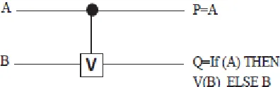
B. Controlled-V and Controlled-V+ Gate
Controlled V and V+ are the basic gates. In the controlled-V gate when the control signal A = 0, then the input B on target line will pass through the controlled part unchanged, that is Q = B. When A = 1, then the unitary operation V is applied to the input B, and output will be Q = V(B).
Fig 2. Quantu m rep res en tatio n o f Co n tro lled -V.
In the controlled-V+ gate when the control
signal A = 0, then the input B will pass through the controlled part unchanged, that is Q = B.
When A = 1, then the unitary operation V+= V-
1 is applied to the input B, that is, Q = V+(B).
Fig 3. Quantum repres en tatio n o f Co n tro lled -V+.
The V and V+ gates have the following
properties:
V×V = NOT V×V+ = V+×V = I
V+×V+ = NOT
C. Controlled-NOT Gate/ Feynman Gate
It is a 2*2 reversible logic gate. CNOT Gate, also known as FEYNMAN Gate. It is used to overcome the fan-out problem since it can be used for copying the information. CNOT gate has unit quantum cost and unit delay.
Fig .4 Feynman gate & its quantum rep res en tatio n .
Toffoli gate is a 3*3 reversible gate with quantum cost of 5 and delay of 5∆. It is called also universal reversible gate.
Fig .5 Toffoli gate and its quantu m rep res en tatio n .
E. Fredkin Gate
Fredkin Gate is also a 3*3 gate. It has 5 quantum cost and delay is 5∆. When A = 0, the other two inputs B and C is simply copied to the output. But when A = 1, B and C is swapped in the output. Hence, it is also denominated as a controlled swap gate. Basic logic function can be implemented using this gate and called universal reversible gate.
Fig 6. Fredkin gate and its quantum repres en tatio n .
F. Peres Gate
Peres gate is a 4-input and 4-output (4*4) reversible gate. It has a minimum quantum cost among the 4*4 reversible gate and is equal to 4 and delay is 4∆.
Fig 7. Peres gate and its q u an tu m rep res en tatio n .
G. Proposed Modified Fredkin (MF) Gate
It is the proposed modified version of 3*3 Fredkin gate with a quantum cost of 4 and a delay of 4∆. When A = 0, it is the same as Fredkin Gate, but when A = 1, B and
complement of C is swapped in the output. Quantum representation of this gate is
Fig 8. MF gate an d its q u an tu m rep res en tatio n .
III.PROPOSED SYSTEM
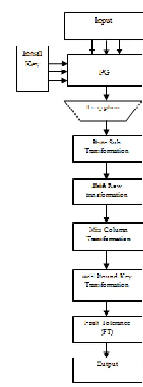
The fig: 9 shows the encryption block diagram with high security implementation. The initial stage having input and initial key goes under PG operation for less power consumption. This conversion of binary data to a matrix is totally carried out by byte sub transformation. Now the total matrix consisting of row and columns by using these we implemented the security by the hybrid crossbar technique.
Shift Row transformation is one of the technique for security i.e. the total row is matrix is shifted to another row and with vice and versa. The second technique is mix column transformation it gives two columns into a single column to reduce the size. In another way we can make as comparison of two columns into a single column.
The add round key transformation is used rounding the nearest value of matrix. This represents the rounded output taken as ‘e’ for encryption block. After that Add round key is given to the Fault Tolerance. Next it is given to the output. The total encryption block is used in the transmitter side. The output of encryption block given to input to decryption block.
Similarly decryption block consisting of sub blocks as encryption with small inversion. So the input ‘e’ taken as input for decryption the input ‘e’ and final key goes under decryption with hybrid crossbar technique and the output of the decryption given to input as for inverse byte sub transformation. The inverse byte sub transformation divide the matrix representation into binary representation.
IV. RESULTS
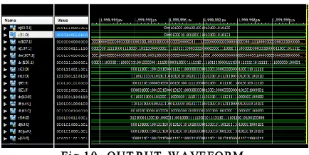
The encryption and decryption is designed by using reversible gates. The total input bits of proposed encryption are multiplexed with the initial key by using Reversible gates. After that the encryption and by sub transformation, shift row mix column, add round key will be given to the input and output pins. Finally, the DD is the output as shown in the graphical representation of fig10.
The total operations of Byte sub transformation,
Shift row transformation, Mix column
transformation, Add round key transformation
and Fault tolerance are operated with reversible gates to make the operation accurately and takes less power for high speed application.
Fig 1 0 . OUT P UT W AVE FORM
V.CONCLUSION
A novel architecture of encryption and decryption using high security technique for the VLSI implementation using Reversible gates is implemented. The pre-defined keys are required for each input for both encryption and decryption that are generated in real-time by the key-scheduler module by expanding the initial secret key and thus used for reducing the amount of storage for buffering. S-boxes are used for the implementation of the S.R, M.C and inverses S.R & M.C shared between encryption and decryption. The round keys needed for each round of the implementation are generated in real-time. The forward and reverse key scheduling is implemented on the same device, thus allowing efficient area minimization. The fault tolerance circuit gives error free output than existed cryptography application. The total design is designed with reversible gates to make less power for high speed application.
VI.REFERENCES
[1] J. Rose et al., “The VTR project:
Architecture and CAD for FPGAs from verilog
to routing,” in Proc. ACM/SIGDA FPGA, 2012,
pp. 77–86.
the CHStone benchmark program suite for practical C-based high-level synthesis,” J. Inf. Process., vol. 17, pp. 242–254, Oct. 2009.
[3] A. Canis et al., “LegUp: High-level synthesis
for FPGA-based processor/accelerator systems,” in Proc. ACM/SIGDA FPGA, 2011, pp. 33–36. [4] E. Ahmed and J. Rose, “The effect of LUT and cluster size on deepsubmicron FPGA
performance and density,” IEEE Trans. Very
Large Scale Integr. (VLSI), vol. 12, no. 3, pp. 288–298, Mar. 2004.
[5] J. Rose, R. Francis, D. Lewis, and P. Chow, “Architecture of fieldprogrammable gate arrays: The effect of logic block functionality on area efficiency,” IEEE J. Solid-State Circuits, vol. 25, no. 5, pp. 1217–1225, Oct. 1990.
[6] H. Parandeh-Afshar, H. Benbihi, D. Novo, and P. Ienne, “Rethinking FPGAs: Elude the flexibility excess of LUTs with and-inverter
cones,” in Proc. ACM/SIGDA FPGA, 2012, pp.
119–128.
[7] J. Anderson and Q. Wang, “Improving logic density through synthesisinspired architecture,” in Proc. IEEE FPL, Aug./Sep. 2009, pp. 105– 111.
[8] J. Anderson and Q. Wang, “Area-efficient FPGA logic elements: Architecture and
synthesis,” in Proc. ASP DAC, 2011, pp. 369–
375.
[9] J. Cong, H. Huang, and X. Yuan, “Technology mapping and architecture evalution
for k/m-macrocell-based FPGAs,” ACM Trans.
Design Autom. Electron. Syst., vol. 10, no. 1, pp. 3–23, Jan. 2005.
[10] Y. Hu, S. Das, S. Trimberger, and L. He,
“Design, synthesis and evaluation of
heterogeneous FPGA with mixed LUTs and
macro-gates,” in Proc. IEEE ICCAD, Nov.
2007, pp. 188–193.
[11] K. Fu and J. Blum, “Controlling for cybersecurity risks of medical device software,”
Commun. ACM, vol. 56, no. 10, pp. 35–37, Oct. 2013.
[12] D. Halperin, T. Kohno, T. S. Heydt-Benjamin, K. Fu, and W. H. Maisel, “Security and privacy for implantable medical devices,”
IEEE Pervasive Comput., vol. 7, no. 1, pp. 30– 39, Jan./Mar. 2008.
AUTHORS DETAILS:
Venkateswara Reddy Peram has
completed her B.Tech in
Electronics and Communication Engineering from Chinthalapudi
Engineering College,J.N.T.U.K
affiliated college in 2013.He is pursuing her M.Tech in VLSI
from Malineni Perumallu
Educational Society , J.N.T.U.K affiliated college.
Sankara Rao Kamineni is an Professor at Malineni Perumallu Educational Society Group of Institutions, Guntur. M.Tech,
ECE from Sree Kavitha