ISSN (Print) : 2320 – 3765 ISSN (Online): 2278 – 8875
I
nternational
J
ournal of
A
dvanced
R
esearch in
E
lectrical,
E
lectronics and
I
nstrumentation
E
ngineering
(A High Impact Factor, Monthly, Peer Reviewed Journal)
Website: www.ijareeie.com
Vol. 6, Issue 10, October 2017
Low Power ASIC Implementation of RSD
Based ECC Processor for Cryptography
Applications
P.Anusha1 , Dr.B.L.Malleswari2
, Mohana Leela3
PG Scholar, Dept. of ECE, SWEC, Hyderabad, TS, India
Principal & Professor, Dept. of ECE, SWEC, Hyderabad, TS, India
Assistant Professor, Dept. of ECE, Hyderabad, TS, India
ABSTRACT- In the Proposed dissertation, it focuses on Application Specific Instruction Set of elliptical curve cryptography processor based on redundant signed digit representation. The processor employs an Efficient Floating-Point Multiplier technique using Karatsuba Urdhva-Triyagbhyam that offers a Superior implementation in terms of delay and area. This Karatsuba Multiplier uses a divide and conquer technique as it divides into MSB and LSB. Where a Karatsuba Multiplier is more efficient for greater bit lengths only and it is not efficient for lesser bit lengths. So, to overcome this problem a proposed multiplier is used Urdhva-Tiryagbhyam Multiplier for lesser bit lengths. Here in the Proposed Design System we go for Urdhva- Tiryagbhyam multiplier to reduce the quantity of phases required for multiplications that can be decreased. The proposed processor performs overall functions and finally reduces the power. I.e..,Low-Power. This processor is implemented in ASIC (Application Specific Integrated Circuit). The main aim of the project is used for Security Purpose ie., to hide the Data. Major requirements are to design the processor with efficient low-Power design. Here Encryption and Decryption process are used in order to hide the data. This Processor is done in 180nm & 90nm Technology.
KEYWORDS: Application Specific Integrated Circuit (ASIC), Elliptical Curve Cryptography (ECC), Karatsuba Urdhva- Tiryagbhyam Multiplier, Redundant Signed Digit (RSD), Low Power.
I. INTRODUCTION
ISSN (Print) : 2320 – 3765 ISSN (Online): 2278 – 8875
I
nternational
J
ournal of
A
dvanced
R
esearch in
E
lectrical,
E
lectronics and
I
nstrumentation
E
ngineering
(A High Impact Factor, Monthly, Peer Reviewed Journal)
Website: www.ijareeie.com
Vol. 6, Issue 10, October 2017
II. PROPOSED PROTECTION SCHEME FOR ECC PROCESSOR
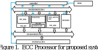
In this System, an elliptical curve cryptography (ECC) processor based on Redundant signed digit (RSD) representation is represented. Here the processor employee’s different techniques for Karatsuba-Ofman method in order to achieve high through put multiplication. The processor mainly consists of an AU of 256 RSD, a finite-state machine (FSM), Memory and two Data buses. As a result, an efficient Modular adder without comparison of 2’s complement and a high-through put modular divider, it results in a shortest data path for maximized frequency are represented. The Processor performs Single point multiplication employing points in affine coordinates in 2.26ms and runs at a maximum frequency of 160 MHZ in Xilinx Vertex 5. Here the Processor is implemented in FPGA (i.e.., Field Programmable Gate Array). As Karatsuba-Ofman Multiplier employs divide and conquer method. Here it divides a given operand into MSB and LSB and this continues until the operand is 8-bit length. Karatsuba multiplier is efficient with greater bit lengths and it is not efficient in lesser bit lengths. So, in order to overcome this problem of lesser bit length we go for proposed Design i.e..,Urdhva- Tiryagbhyam multiplier.
Figure 1. ECC Processor for proposed system
Low Power, Area & Delay are disadvantages in the proposed system.
So, in order to overcome this problem, we go for Extension System Design to achieve low power Implementation.
III. EXTENSION PROTECTION SCHEME FOR ECC PROCESSOR
Here in the Proposed Design System we go for Urdhva- Tiryagbhyam multiplier to reduce the quantity of phases required for multiplications that can be decreased [6]. Here an Efficient floating-point multiplier is used. Urdhva- Tiryagbhyam multiplier is used to implement a binary multiplier for mantissa multiplication. It is finest algorithm for binary multiplications in terms of area and delay.Thus, Urdhva-Tiryagbhyam algorithm doesn’t suit well if the input bit length is more. Thus, if we use Karatsuba at greater bit length and Urdhva-Tiryagbhyam algorithm at lesser bit length then then we can compensate the limitations of the algorithm at a greater efficient . By designing the whole processor architecture, we can reduce the Power at lower efficient. Hence Low-Power is being achieved.
BLOCK DIAGRAM AND OPERATION OF THE PROCESSOR
The basic block diagram ie., overall processor architecture consists of an AU of 256 RSD digits (Urdhva-Tiryagbhyam Multiplier, Add/Sub and Division), an finite-state machine (FSM), Memory and two buses. The architecture is shown below.
ISSN (Print) : 2320 – 3765 ISSN (Online): 2278 – 8875
I
nternational
J
ournal of
A
dvanced
R
esearch in
E
lectrical,
E
lectronics and
I
nstrumentation
E
ngineering
(A High Impact Factor, Monthly, Peer Reviewed Journal)
Website: www.ijareeie.com
Vol. 6, Issue 10, October 2017
OPERATION: The Processor architecture contains mainly AU (Arithmetic Unit), Control Unit and Instruction Set. Here two sub-control units are attached to the main control unit as add-on-blocks. Different coordinate systems are easily supported by adding corresponding sub control blocks that operate according to the formulae of the coordinate system. Here now the external data is sent through the external data bus to 256RSD digits as input bus. Data is sent as binary format and a binary to RSD converter stuffs zeros in between the binary bits in order to create the RSD representation. As a result, 256-bits binary data represented as binary data are converted to 512-bits RSD represented integers.
DESCRIPTION OF EACH BLOCKS IN A PROCESSOR RSD (REDUNDANT SIGNED DIGIT)
RSD is a numerical system which is used for signed digits. It uses more number of bits than a single bit representation. It is a carry free arithmetic as the integers are represented by the difference of two other integers. Here let us consider X as an integer than it is represented by the difference of .RSD is widely used in the integer format as it performs addition and subtraction operations without using 2s compliment. Here the binary digits are used such as 0 and 1. In radix-2, RSD we represent integers of either +1,0 or -1.
ARITHMETIC UNIT
The Arithmetic Unit plays a major role in designing a processor as it is the core of a processor architecture that includes different blocks. The different blocks of Arithmetic Unit are given below:
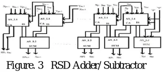
MODULAR ADDITION / SUBTRACTION BLOCK
Here we are representing a RSD based ECC Processor. So, a carry free adder is being used. In radix-2 RSD we represent integers such as either of +1, 0 or -1. Each integer has been coded with a binary digit as
‘0’ is coded with ‘00’, ‘1’is coded with ‘10’ and ‘-1’is coded with ‘01’.
Figure. 3 RSD Adder/ Subtractor
ISSN (Print) : 2320 – 3765 ISSN (Online): 2278 – 8875
I
nternational
J
ournal of
A
dvanced
R
esearch in
E
lectrical,
E
lectronics and
I
nstrumentation
E
ngineering
(A High Impact Factor, Monthly, Peer Reviewed Journal)
Website: www.ijareeie.com
Vol. 6, Issue 10, October 2017
Figure.4 Modular Addition Subtraction Block Diagram.
The above block diagram consists of One full word RSD Adder, two full word multipliers, and one register with some control signals.
KARATSUBA URDHVA- TIRYAGBHYAM MULTIPLIER
Karatsuba Urdhva-Tiryagbhyam Multiplier works as more efficient multiplier. Here the processor employs different techniques for Karatsuba-Ofman method and Urdhva-Triyagbhyam Multiplier in order to achieve high through put multiplication [09]. Karatsuba-Ofman Multiplier employs divide and conquer method. Here it divides a given operand into MSB and LSB and this continues until the operand is 8-bit length. Karatsuba multiplier is efficient with greater bit lengths and it is not efficient in lesser bit lengths. So, in order to overcome this problem of lesser bit length we go for proposed Design i.e..,Urdhva- Tiryagbhyam multiplier. Here Urdhva- Tiryagbhyam multiplier reduce the quantity of phases required for multiplications that can be reduced. Urdhva- Tiryagbhyam multiplier is used to implement a binary multiplier for mantissa multiplication. If we try to compensate the delay, then it will cause the increases in area. Thus, Urdhva-Tiryagbhyam algorithm doesn’t well if the input bit length is more. Thus, if we use Karatsuba at greater bit length and Urdhva-Tiryagbhyam algorithm at lesser bit length then then we can compensate the limitations of the algorithm at a greater efficient. By designing the whole processor architecture, we can reduce the Power. Hence Low-Power is being achieved.
Figure.5 Karatsuba Urdhva-Tiryagbhyam Binary Multiplier
Line diagram for Urdhva-Tiryagbhyam Binary Multiplier is given step by step process below. Let us consider an example of two-4bit numbers ie., P3, P2,P1,P0 and Q3, Q2,Q1,Q0 and the products be R7,R6,R5,R4,R3,R2,R1,R0 with temporal partial products as S0,S1,S2,S3,S4,S5,S6.The partial products obtained are given below.
Step 1: S0=P0Q0
Step 2: S1= P1 Q0 + P0 Q1
Step 3: S2= P2 Q0 + P1 Q1 + P0 Q0 Step 4: S3= P3 Q0+ P2 Q1 + P1 Q2+ P0 Q3 Step 5: S4= P3 Q1+ P2 Q2+ P1 Q3
Step 6: S5= P3 Q2+ P2 Q3 Step 7: S6= P3 Q3
Here the products are obtained by adding T1,T2,T3 where T1,T2,T3 are the partial sums. Ie., T1= S6 S5[0] S4[0] S3[0] S2[0] S1[0] S0
ISSN (Print) : 2320 – 3765 ISSN (Online): 2278 – 8875
I
nternational
J
ournal of
A
dvanced
R
esearch in
E
lectrical,
E
lectronics and
I
nstrumentation
E
ngineering
(A High Impact Factor, Monthly, Peer Reviewed Journal)
Website: www.ijareeie.com
Vol. 6, Issue 10, October 2017 Product= S6 S5[0] S4[0] S3[0] S2[0] S1[0] S0 +
S5[1] S4[1] S3[1] S2[1] S1[1] 0 + S3[2] 0 0 0 --- R7 R6 R5 R4 R3 R2 R1 R0
MODULAR DIVISION
Modular Division is an efficient way of performing in the GCD as it is based on addition, subtraction, and shifting Operation. Mainly Complexity occurs due to the running time and its input dependent [11].In the Step 1, the divider is checked whether it is Odd or Even .In the Step2, the contents in the Register are Swapped according to the flag.In the Step3, the division by 4 modulo M is performed.
Figure.6 Modular Divider
The block diagram mainly consists of three RSD adders, 3*1 Multiplexers, Registers and a Control Processor with some Logic. First, division by 2 or by 4 is performed by shifting 1-digit/2-digits based on the LSDs are Zeros. Division by 2 Modulo M (division by 4 modulo M) is executed by adding or subtracting the dividend to or from the modulus. Here we must check whether the dividend is even or odd and the value of M. Here two parameters are checked ie., delta
( ) and rho(ρ). Here comparison is made with 0 necessary. Here a flag is used to control the shift direction of, where
the flag and the value of LSB are used to determine as it is less than the zero or not.
CONTROL UNIT AND INSTRUCTION SET
The Control unit consists of FSM (ie., Finite State Machine). Here different Scalar point multiplications are supported at instruction level/set.
MAIN CONTROLLER
The Main Controller is used for Fetching, Reading and for execution purpose from Memory [12]. By the flow of instructions, the two attached processing units for point addition and point doubling are controlled accordingly. AU blocks and Memory blocks are generated at the running time of point addition and point doubling of control signals. Here the operation is mainly controlled via flag signals coming from the AU blocks. Main controller is just an FSM where instructions are listed in the instruction set shown in the fig below given.
Figure.7 Main controller
ISSN (Print) : 2320 – 3765 ISSN (Online): 2278 – 8875
I
nternational
J
ournal of
A
dvanced
R
esearch in
E
lectrical,
E
lectronics and
I
nstrumentation
E
ngineering
(A High Impact Factor, Monthly, Peer Reviewed Journal)
Website: www.ijareeie.com
Vol. 6, Issue 10, October 2017
Here the FSM reaches the Finite State where the output coordinates are loaded to output and the processor goes back to its initial state.
ROM & INSTRUCTION SET
Instruction Set is used at multiplication level, where it represents point addition and point doubling operations. We can also implement Instruction Set in arithmetic level. As a result, the Complexity gets increased and cost also increases. The regular point addition requires 6 additions, 2 multiplications and 1 divisions, whereas point doubling requires 8 additions, 3 multiplications and 1 division. The Table below shows the Instruction Set with their operations and hexadecimal codes along with the clock cycles and their timings.
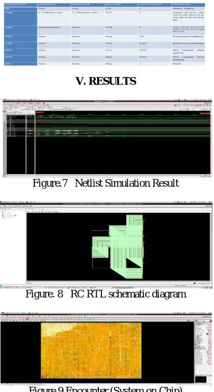
V. RESULTS
Figure.7 Netlist Simulation Result
Figure. 8 RC RTL schematic diagram
ISSN (Print) : 2320 – 3765 ISSN (Online): 2278 – 8875
I
nternational
J
ournal of
A
dvanced
R
esearch in
E
lectrical,
E
lectronics and
I
nstrumentation
E
ngineering
(A High Impact Factor, Monthly, Peer Reviewed Journal)
Website: www.ijareeie.com
Vol. 6, Issue 10, October 2017
THE OUTPUTS OF ENCRYPTION AND DECRYPTION IS GIVEN BELOW
Original Image
Encrypted image
From the above fig., the Original data ie., ‘HELLO’ is given as an input and it is encrypted in an image.
Here a noisy image is selected. since after encrypting, the encrypted part will seem totally noisy as above shown. So, an image will serve as a better camouflage. Keep it in mind that this original image will be your password to decrypting the coded image. So, keep it safe. Here in My file text ‘HELLO’ is given. This data is now encrypted and hidden in an image.
Original image
Encrypted image
‘HELLO’ Decrypted Output
Here from above diagram decrypted output can be seen.
Decryption is the reverse process of encryption. Here the data is decrypted and finally we get original data as ‘HELLO’ as the input is given as ‘HELLO’.
COMPARISON REPORTS ON TECHNOLOGY BASED ie., 180NM & 90NM
Table.1 Results in tabular of Extension in 180nm & 90nm Technology
SNo. TECHNOLOGY POWER (nanoWatt) AREA
( )
1 90nm 24934893.266 594341
ISSN (Print) : 2320 – 3765 ISSN (Online): 2278 – 8875
I
nternational
J
ournal of
A
dvanced
R
esearch in
E
lectrical,
E
lectronics and
I
nstrumentation
E
ngineering
(A High Impact Factor, Monthly, Peer Reviewed Journal)
Website: www.ijareeie.com
Vol. 6, Issue 10, October 2017
Table. 2 Results in tabular form of Proposed in 180nm & 90nm Technology
COMPARISON REPORT OF PROPOSED & EXTENSION IN 90NM TECHNOLOGY
Table.3 There is a decrease in Power
SNo. NAME OF THE
SYSTEM
POWER (nanoWatt) AREA ( )
1 EXTENSION 24934893.266 594341
2 PROPOSED 28008103.933 515050
VI. APPLICATION OF ECC PROCESSOR
Elliptical Curve Cryptography is a technique which is used to approach a public and private key techniques based on elliptical curves over a finite field. This theory that can create faster, smaller and more efficient Cryptography keys. Cryptography is mainly used for security purpose.
Figure.10 Encryption and Decryption Block Diagram
Operation of block diagram: From above Fig., a Plain text is taken as input and this plain text is being encrypted by encryption algorithm. Here after the text is been encrypted it is hided in secret key and this secret key is processed in the processor and the resultant encryption output i.e..,hidden data/ image/video is given to cipher text. From cipher text the encrypted data is given to secret key and there it processes by the decryption algorithm and thus final output is formed i.e.., Original Plain text.
SNo. TECHNOLOGY POWER (nanoWatt) AREA ( )
1 90nm 28008103.933 515050
ISSN (Print) : 2320 – 3765 ISSN (Online): 2278 – 8875
I
nternational
J
ournal of
A
dvanced
R
esearch in
E
lectrical,
E
lectronics and
I
nstrumentation
E
ngineering
(A High Impact Factor, Monthly, Peer Reviewed Journal)
Website: www.ijareeie.com
Vol. 6, Issue 10, October 2017
VII. CONCLUSION
This paper Processor has proposed the ASIC implementation of the elliptical curve cryptography processor for Security applications and this technique ie., cryptography is widely used in many real-time applications. Here we have used for Encryption and Decryption purpose to secure/hide the data. When comparing with the previous proposed background they have implemented in FPGA and used Karatsuba Multiplier. This Karatsuba Multiplier uses a divide and conquer technique as it divides into MSB and LSB. Where a Karatsuba Multiplier is more efficient for greater bit lengths only and it is not efficient for lesser bit lengths. So, to over this problem a proposed multiplier is used Urdhva-Tiryagbhyam Multiplier for lesser bit lengths. Hence, we compensated the limitations of both the algorithms and designed a Karatsuba Urdhva-Tiryagbhyam Multiplier for more efficiency and the Multiplier becomes more efficient.The implementation results of the proposed processor as resulted in gaining Low-Power. Which is the fastest reported in the literature for ECC processors with ASIC design.
VIII. FUTURE SCOPE
To evaluate the practicality of the proposed project we can even achieve it in images and speeches. As in proposed project we have done encryption and decryption by taking input as data message. In future, we can even take image and speech messages as input for encrypting and decrypting. Here in proposed paper we have done in 180 nm and 90nm technology. There is a huge scope in doing this paper in 45nm technology also. Here by using different arithmetic unit techniques (addition, subtraction multiplication and division) we can modify Processor. We can also use this Urdhva-Tiryagbhyam Multiplier in for two variable multipliers using KCM and Vedic mathematics. And in application purpose we can use it in images and speeches. In this paper, we survey the various implementation approaches with the aim of providing a useful reference for hardware designers for building efficient ECC processors.
REFERENCES
[1] N. Koblitz, “Elliptic curve cryptosystems,” Math. Comput., vol. 48, no. 177, pp. 203–2s09, Jan. 1987.
[2] Koblitz, A.H., Koblitz, N. and Menezes, A. (2011) Elliptic Curve Cryptography: The Serpentine Course of a Paradigm Shift. Journal of Number
Theory, 131, 781-814.
http://dx.doi.org/10.1016/j.jnt.2009.01.006 [Citation Time(s):1]
[3] Liddell, Henry George; Scott, Robert; Jones, Henry Stuart; McKenzie, Roderick (1984). A Greek-English Lexicon. Oxford University Press. [4] Bellare, Mihir; Rogaway, Phillip (21 September 2005). "Introduction". Introduction to Modern Cryptography. p. 10.
[5] A.Avizienis, ‘‘signed-digit numbe representations for fast parallel arithmetic,’’ IRE Trans. Electron. Compu.., vol. EC-10, no. 3, pp. 38-400, sep,1961.
[6] Booth, A.D., “A signed binary multiplication technique,” Quarterly Journal of Mechanics and Applied Mathematics, vol. 4, pt. 2, pp. 236– 240, 1951.
[7]http://wwwee.eng.hawaii.edu/~tep/EE150/book/chap1/subsection2.1.2.1.html
[8] Phatak, Dhananjay S.; Koren, Israel (August 1994). "Hybrid Signed-Digit Number Systems: A Unified Framework for Redundant Number Representations with Bounded Carry Propagation Chains" (PDF). IEEE Transactions on Computers. 43 (8): 880–891. doi:10.1109/12.295850 [09] A. Karatsuba and Yu. Ofman (1962). "Multiplication of Many-Digital Numbers by Automatic Computers". Proceedings of the USSR Academy of Sciences. 145: 293–294. Translation in the academic journal Physics-Doklady, 7 (1963), pp. 595–596.
[10] A. A. Karatsuba (1995). "The Complexity of Computations" (PDF). Proceedings of the Steklov Institute of Mathematics. 211: 169–183. Translation from Trudy Mat. Inst. Steklova, 211, 186–202 (1995).
[11] Thapliyal and H.R Arbania. “A Time-Area-Power Efficient Multiplier and Square Architecture Based On Ancient Indian Vedic Mathematics”, Proceedings of the 2004 International Conference on VLSI (VLSI’04), Las Vegas, Nevada, June 2004, pp. 434-439.
[12] von Neumann, John (1945), First Draft of a Report on the EDVAC (PDF), Moore School of Electrical Engineering, University of Pennsylvania, archived from the original (PDF) on March 14, 2013.
ISSN (Print) : 2320 – 3765 ISSN (Online): 2278 – 8875
I
nternational
J
ournal of
A
dvanced
R
esearch in
E
lectrical,
E
lectronics and
I
nstrumentation
E
ngineering
(A High Impact Factor, Monthly, Peer Reviewed Journal)
Website: www.ijareeie.com
Vol. 6, Issue 10, October 2017
BIOGRAPHY
Ms. Anusha. Pallye has completed B. TECH in ECE Department from Jagruti Institute of Engineering & Technology, Ibrahimpatnam Hyderabad. Presently pursuing Masters in VLSI System Design in Sridevi Women‟s Engineering College, Vattina-gulapally, Gandipet, Hyderabad, India.
Dr.B.L.Malleswari working as professor and Principal in Sridevi Women’s Engineering college. She has got 80 National and International Conferences. Also 40 National and international publications. She is specialized in communications and GPS.
Miss.Mohana Leela working as Assistant Professor in Sridevi Women’s Engineering college