ISSN (Print) : 2320 – 3765 ISSN (Online): 2278 – 8875
I
nternational
J
ournal of
A
dvanced
R
esearch in
E
lectrical,
E
lectronics and
I
nstrumentation
E
ngineering
(An ISO 3297: 2007 Certified Organization) Vol. 4, Issue 4, April 2015
Highly Optimized APC-OMS Based Recursive
Least Square (RLS) Adaptive Filter with Fast
Convergence Rate
Sivasakthi S
1, Kalaimani K
2Associate Professor, Dept. of EEE,Krishnasamy College of Engineering and Technology, Cuddalore, Tamilnadu, India1
PG Student [EST], Dept. of EEE, Krishnasamy college of Engineering and Technology, Cuddalore, Tamilnadu, India 2
ABSTRACT: The Recursive Least Square (RLS) adaptive filter is the most popular and widely used adaptive filter not only because of its simplicity but also because of its satisfactory convergence performance. Memory based structures are used in many kind of Digital Signal Processing (DSP) application. Memory-based structures are better performance in area minimization compare with multiply-accumulate structures and have many other advantages such as reduced latency. The Anti-Symmetric Product Coding (APC) and Odd-Multiple-Storage (OMS) techniques were used for Look-Up-Table (LUT) in adaptive FIR filter. Memory-based structure such as APC and OMS techniques are used for efficient low power design using LUT partitioning. Hence, the combination of these two techniques provides reduction in LUT size to one-fourth in adaptive FIR filter when compared with the conventional Look -Up -Table (LUT) of adaptive FIR filter.
KEYWORDS:Anti-symmetric product coding, Odd multiple storage, Look-up-table, Recursive least square ,Adaptive FIR filter.
I. INTRODUCTION
A conventional look-up-table (LUT)-based multiplier is shown in Table.1, where A is a fixed coefficient, and X is an input word to be multiplied with A. Assuming X to be a positive binary number of word length L, there can be 2L
possible values of X, and accordingly, there can be 2L possible values of product C = A ・ X.
Therefore, for memory-based multiplication, an LUT of 2L words, consisting of pre computed product values corresponding to all possible values of X, is conventionally used. The product word A ・ Xi is stored at the location Xi
for 0 ≤ Xi ≤ 2L − 1, such that if an L-bit binary value of Xi is used as the address for the LUT, then the corresponding product value A ・ Xi is available as its output.
A. LUT’s in FPGAs
Three ways of using RAM blocks as multipliers are available. They are basic single look-up table multiplier, partial product multiplier, and RAM based constant coefficient multiplier. For the Accelerator devices, the single look-up-table approach can create a very fast, but narrow, 4-bit multiplier.
B. Basic Look-Up Table (LUT)-Based Multipliers
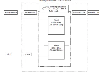
Fig.1 Storage and Demonstrates A 4×4 Bit Multiplier
Since the memory block in the accelerator is synchronous, this configuration will result in a synchronous multiplier. The multiplier’s clock frequency is only limited by the data access time of the memory. This approach is more efficient than implementing multipliers in gates, but it can consume a large amount of memory. The amount of memory required increases with the square of the bit width.
C. PARTIAL PRODUCT MULTIPLIERS
One way to mitigate the amount of memory required is to use partial product multiplication. This technique combines the look-up table approach with elements of longhand multiplication. For example, to multiply 24 × 43 = 1032 using longhand, we simplify the problem into the sum of 4 multiplication functions and three addition functions (4×3 + ((2×3) ×10)) + ((4×4) + ((2×4) ×10) ×10) = 1032.
Fig. 2 Constant Coefficient Multiplier
D. CONSTANT COEFFICIENT MULTIPLIER
A third approach to using memory blocks as multipliers is employing a constant coefficient multiplier. In many cases, especially in Digital Signal Processing (DSP) applications, the multiplicand remains constant and only the multiplier varies. Although can create a constant coefficient multiplier using pure logic, implementing this function in RAM creates a much faster multiplier and uses very few logic gates.
ISSN (Print) : 2320 – 3765 ISSN (Online): 2278 – 8875
I
nternational
J
ournal of
A
dvanced
R
esearch in
E
lectrical,
E
lectronics and
I
nstrumentation
E
ngineering
(An ISO 3297: 2007 Certified Organization) Vol. 4, Issue 4, April 2015
This type of multiplier scales linearly with the width of the values being multiplied. While a basic look-up table 8×8 multiplier uses one block of 65536×16 bit words, 128 Kbytes of storage, and the partial product look-up table multiplier uses four blocks of 256×8 bit words, 1 Kbyte, the constant coefficient multiplier requires only one block of 256×16 bit words, 0.5 Kbyte, and does not incur the cost of the additional logic and delay incurred by using the partial product multiplier.
II. DESIGNMETHODOLOGY
A. APC FOR LUT OPTIMIZATION
In addition, the sum of product values corresponding to these two input values on the same row is 32A. Let the product values on the second and fourth columns of a row be u and v,respectively. Since one can write u = [(u + v)/2 − (v − u)/2] and v = [(u + v)/2 + (v − u)/2], for (u + v) = 32A, we can have
.
Fig.4 Proposed APC–OMS combined LUT design
Product word = 16A + (sign value) × (APC word) where sign value = 1 for x4 = 1 and sign value = −1 for x4 = 0. The product value for X = (10000) corresponds to APC value “zero,” which could be derived by resetting the LUT output, instead of storing that in the LUT.
Fig.5 LUT-based multiplier for L = 5 using the APC technique
III.MODIFIEDOMSFORLUTOPTIMIZATION
for the multiplication of any binary word X of size L, with a fixed coefficient A, instead of storing all the 2L possible values of C = A ・ X, only (2L/2) words corresponding to the odd multiples of A may be stored in the LUT, while all the even multiples of A could be derived by left-shift operations of one of those odd multiples
.
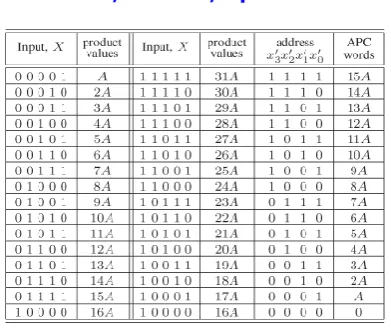
A. APC words for different input value
Table.1 APC words for different input values
1)A memory unit of [(2L/2) + 1] words of (W + L)-bit width is used to store the product values, where the first (2L/2) words are odd multiples of A, and the last word is zero.
2) A barrel shifter for producing a maximum of (L − 1) left shifts is used to derive all the even multiples of A.
3) The L-bit input word is mapped to the (L − 1)-bit address of the LUT by an address encoder, and control bits for the barrel shifter are derived by a control circuit.
D. OMS-based design of the LUT of APC words
Table .2 OMS-based design of the LUT of APC words
The word to be stored for X = (00000) is not 0 but 16A, which we can obtain from A by four left shifts using a barrel shifter. However, if 16A is not derived from A, only a maximum of three left shifts is required to obtain all other even multiples of A. A maximum of three bit shifts can be implemented by a two-stage logarithmic barrel shifter, but the implementation of four shifts requires a three-stage barrel shifter. For X = (10000), the APC word “0” is derived by
resetting the LUT output, by an active-high RESET signal given by
ISSN (Print) : 2320 – 3765 ISSN (Online): 2278 – 8875
I
nternational
J
ournal of
A
dvanced
R
esearch in
E
lectrical,
E
lectronics and
I
nstrumentation
E
ngineering
(An ISO 3297: 2007 Certified Organization) Vol. 4, Issue 4, April 2015
IV.PROPOSEDLUTOPTIMIZATIONSCHEME
A. LUT Multiplier Using APC
The structure and function of the LUT-based multiplier for L = 5 using the APC technique. It consists of a four-input LUT of 16 words to store the APC values of product words as given in the sixth column of Table.1, except on the last row, where 2A is stored for input X = (00000) instead of storing a “0” for input X = (10000). Besides, it consists of an address-mapping circuit and an add/subtract circuit.
B. LUTUSING MODIFIED OMS
The proposed APC–OMS combined design of the LUT for L = 5 and for any coefficient width W. It consists of an LUT of nine words of (W + 4)-bit width, a four-to-nine-line address decoder, a barrel shifter, an address generation circuit, and a control circuit for generating the RESET signal and control word (s1s0) for the barrel shifter.while 2A is stored for input X = (00000) at LUT address “1000,” as specified in Table 3.2. The decoder takes the 4-bit address from the
address generator and generates nine word-select signals, i.e., {wi, for 0 ≤ i ≤ 8}, to select the referenced word from the LUT.
Fig .6 (a) sign modification LUT output. (b) Address-generation circuit.
The control bits s0 and s1 to be used by the barrel shifter to produce the desired number of shifts of the LUT output are generated by the control circuit, according to the relations
Note that (s1s0) is a 2-bit binary equivalent of the required number of shifts specified in Tables 3.1 and 3.2.
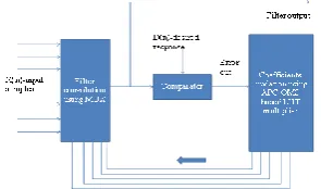
C. BLOCK DIAGRAM OF ADAPTIVE FIR FILTER
Fig.7 Block Diagram for Adaptive Filter
Adaptive filters differ from other filters such as FIR and IIR in the sense that
The coefficients are not determined by a set of desired specifications
The coefficients are not fixed.
Applications include: process control, medical instrumentation, speech processing, echo and noise calculation and channel equalization.
V. RESULTSANDDISCUSSION MODULES:
A. Performance of RLS B. Power analyser C. Synthesis report
A.PERFORMANCE OF RLS
Fig. 8 Simulated output
In the fig.8, shows the Convergence performance of system identification with RLS.
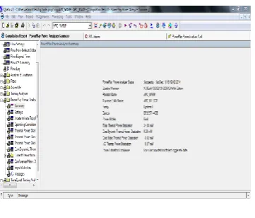
B.POWER ANALYZER
Fig. 9 Flow summary report
In the fig.9, show the power analyser with the help of QUARATUS-II software.
POWER ANALYZER
Table.1 power analyzer
OVERCOME VALUES
Existing System 60.52Mw
ISSN (Print) : 2320 – 3765 ISSN (Online): 2278 – 8875
I
nternational
J
ournal of
A
dvanced
R
esearch in
E
lectrical,
E
lectronics and
I
nstrumentation
E
ngineering
(An ISO 3297: 2007 Certified Organization) Vol. 4, Issue 4, April 2015
In this tabulation.1, show the different between existing system and proposed system.
D. SYNTHESIS REPORT
Fig.10 RTL Schematic report for efficient FIR filter
In this fig.10 show the area minimization with the help of APC-OMS techniques.
VI.CONCLUSION
In this paper simulation is carried out by using the APC-OMS based multiplier to reduce total logical area consumption. The Anti-Symmetric Product Coding (APC) and Odd-Multiple-Storage (OMS) techniques were used for Look-Up-Table (LUT) FIR filter. Hence, the combination of these two techniques provides reduction in LUT size to one-fourth in adaptive FIR filter, it improving the convergence performance of system identification by using Recursive Least Square approach, synthesis the performance of power and timing analyzer.
REFERENCES
1. J.-I. Guo, C.-M. Liu, and C.-W. Jen, “The efficient memory-based VLSI array design for DFT and DCT,” IEEE Trans. Circuits Syst. II, Analog Digit. Signal Process., vol. 39, no. 10, pp. 723–733, Oct. 1992
2. H.-R. Lee, C.-W. Jen, “On the design automation of the memory-based VLSI architectures for FIR filters,” IEEE Trans. Consum. Electron., vol. 39, no. 3, Aug. 1993
3. D. F. Chiper, M. N. S. Swamy, M. O. Ahmad, and T. Stouraitis, “A systolic array architecture for the discrete sine transform,” IEEE Trans. Signal Process., vol. 50, no. 9, pp. 2347–2354, Sep. 2002.
4. H.-C. Chen, J.-I. Guo, T.-S. Chang, and C.-W. Jen, “A memory-efficient realization of cyclic convolution and its application to discrete cosine transform,” IEEE Trans. Circuits Syst. Video Technol., vol. 15, no. 3, pp. 445–453, Mar. 2005
5. D. F. Chiper, M. N. S. Swamy, M. O. Ahmad, and T. Stouraitis, “Systolic algorithms and a memory-based design approach for a unified architecture for the computation of DCT/DST/IDCT/IDST,” IEEE Trans. Circuits Syst. I, Reg. Papers, vol. 52, no. 6, pp. 1125–1137, Jun. 2005.
6. P. K. Meher, “Systolic designs for DCT using a low-complexity concurrent convolutional formulation,” IEEE Trans. Circuits Syst. Video Technol., vol. 16, no. 9, pp. 1041–1050, Sep. 2006.
7. P. K. Meher, “Memory-based hardware for resource-constrained digital signal processing systems,” in Proc. 6th Int. Conf. ICICS, Dec. 2007, pp. 1–4.
BIOGRAPHY
Kalaimani.K has received her B.E. (ECE) in the year 2012 from Vivekanandha Institute of