Patterning: Principles and Some New
Developments**
By
Matthias Geissler
and
Younan Xia*
1. Introduction
Patterning is of paramount importance in many areas of modern science and technology, with applications ranging from the production of integrated circuits, information storage devices, and display units to the fabrication of micro-electromechanical systems (MEMS), miniaturized sensors, microfluidic devices, biochips, photonic bandgap crystals, micro-optical components, and diffractive optical elements.[1] The process of patterning is also commonly referred to as lithography, which involves a flow of information that typical-ly begins with the design of a pattern in the form of a dataset
and ends at a patterned array of features on the surface of a substrate. There can be many steps in between, and each one of these steps may impose the possibility of losing information or pattern distortion. In general, a lithographic technique is built upon the following key elements: i) a pre-designed set of patterns in the form of a mask or a master; ii) a means to mediate the transfer or replication of patterns; iii) a respon-sive medium, which is usually a functional material capable of serving as the resist for subsequent steps; and iv) tools that ensure appropriate metrology.
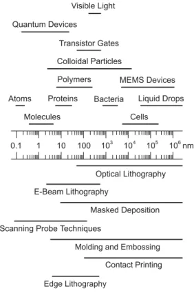
Depending on the application, the requirements for a suc-cessful lithographic process can vary substantially. The critical feature size of the test patterns is probably the most obvious (but not the only) issue one must consider when selecting a proper lithographic technique (Fig. 1). The fabrication of inte-grated circuits, information storage devices, or display units often involves many lithographic steps and demands the use of sophisticated technologies to meet the stringent require-ments in terms of throughput, overlay accuracy, and resolu-tion.[1]The growing demand for higher densities of integra-tion, less power consumpintegra-tion, better performance, and reduction in cost has been and still is the main driving force behind the continuous trend in downsizing the critical
dimen-This article provides an overview of various patterning methodologies,
and it is organized into three major sections: generation of patterns,
replication of patterns, and three-dimensional patterning. Generation of
patterns from scratch is usually accomplished by serial techniques that are
able to provide arbitrary features. The writing process can be carried out in many different ways. It
can be achieved using a rigid stylus; or a focused beam of photons, electrons, and other energetic
particles. It can also be accomplished using an electrical or magnetic field; or through localized
add-on of materials such as a liquid-like ink from an external source. In addition, some ordered
but relatively simple patterns can be formed by means of self-assembly. In replication of patterns,
structural information from a mask, master, or stamp is transferred to multiple copies with the use
of an appropriate material. The patterned features on a mask are mainly used to direct a flux of
radiation or physical matter from a source onto a substrate, whereas a master/stamp serves as the
original for replication based on embossing, molding, or printing. The last section of this article
deals with three-dimensional patterning, where both vertical and lateral dimensions of a structure
need to be precisely controlled to generate well-defined shapes and profiles. The article is
illustrated with various examples derived from recent developments in this field.
±
[*] Prof. Y. Xia, Dr. M. Geissler
Department of Chemistry, University of Washington Seattle, WA 98195±1700 (USA)
E-mail: [email protected]
[**] This work has been supported in part by a Career Award from the NSF (DMR-9983893), an AFOSR-MURI grant awarded to the UW, and a Fellowship from the David and Lucile Packard Foundation. Y. Xia is an Alfred P. Sloan Research Fellow (2000) and a Camille Dreyfus Teacher Scholar (2002). We thank Jesse T. McCann for his proof reading of the manuscript.
sions of semiconductor devices. To this end, the number of transistors on a chip doubles every 18 months, and with the continuation of this trend, densities beyond 1 billion transis-tors/cm2could be achieved in the foreseeable future.[2]Similar trends toward higher levels of complexity and integration may also be found in other applications such as fabrication of MEMS, sensors, microfluidic devices, and biochips.[3±5]In any case, continuous advances in establishing appropriate pattern-ing techniques continue to be the prerequisite for the success of these developments.
Optical lithography is probably the best-established tech-nology for patterning.[6]It has its foundations in microelec-tronics, where it is used for the fabrication of integrated cir-cuits. In optical lithography, a photosensitive film is patterned first by exposure to a spatially modulated UV-light to gener-ate a sacrificial mask for subsequent processing steps. Transfer of patterns from the resist into the underlying substrate can be accomplished by a number of techniques that include selective growth of a material in the unmasked areas of the substrate, and etching or implantation doping through voids in the mask. Photoresists are usually based on organic poly-mers, whose chains are either crosslinked, degraded, or forced to go through molecular rearrangements when they are exposed to energetic species.[7]When a positive-tone resist is illuminated with photons of suitable wavelengths, it will be-come soluble in a developing solution; while a negative-tone resist will show the opposite response and become insoluble upon illumination. Although photolithography works
phe-REVIEWS
Figure 1.Patterning on various length scales. The scale bar indicates the
range of dimensions for a specific object (above the ruler), and the range of feature sizes that have been demonstrated for each type of patterning technique (below the ruler).
Matthias Geissler was born in Leipzig (Germany) in 1972. He received both his M.S. and Ph.D. degrees in chemistry from the University of Jena (Germany). He worked as a research associate at the IBM Zurich Research Laboratory in Rüschlikon (Switzerland) for four years before he came to the University of Washington for a postdoctoral appointment with Prof. Younan Xia in 2003. His research interests include self-assembled monolayers, soft lithography, and materials science. Younan Xia was born in Jiangsu, China, in 1965. He received a B.S. degree in chemical physics from the University of Science and Technology of China (USTC) in 1987, and then worked as a graduate student on nonlinear optical materials for four years at the Fujian Institute of Research on the Structure of Matter, Academia Sinica. He came to the United States in 1991, received a M.S. degree in inorganic chemistry from the University of Pennsylvania (with Prof. A. G. MacDiarmid) in 1993, and a Ph.D. degree in physical chemistry from Harvard University (with Prof. G. M. Whitesides) in 1996. He stayed at Harvard and worked as a postoctoral fellow with Professors G. M. Whitesides and M. Prentiss. He moved to Seattle in 1997 and started as an Assistant Professor of Chemistry at the University of Washington. He was promoted to the rank of tenured Associate Professor in 2001 and to the rank of Professor in 2003. His research interests include nanostructured materials, self-assembly, photonic crystals, colloidal chemistry, microfabrication, surface modification, conduct-ing polymers, microfluidic and microanalytical systems, and novel devices for photonics, optoelectronics, and displays.
nomenally well for many fabrication tasks, it is certainly not the only or best option for all applications. For instance, it can only be applied to directly pattern a limited set of functional materials such as photoresists; it provides little control over the surface functionality; and it is poorly suited for three-di-mensional (3D) fabrication. These limitations have prompted the development of many alternative and complementary methods for patterning,[8]that differ in the way in which the features of interest are generated.
This article intends to provide a general and methodological review of the various techniques for patterning. We do not aim to cover in depth all the technical details of these pattern-ing techniques or to describe their extended and sophisticated variants. It is also impossible to exhaust all types of materials that can be patterned using a specific lithographic method. The focus of this article is to illustrate the different opera-tional and mechanistic principles involved in defining a pat-tern on a substrate. As limited by space, the work included here only represents a selective rather than comprehensive overview of recent advances based on what is available in the literature. In organizing this article, we have divided the task of patterning into two separate tracks: generation and replica-tion of patterns. These two tracks are usually different in terms of characteristics, requirements, and aspects of empha-sis. For example, generation of patterns is commonly achieved in a serial fashion using techniques that are relatively slow, which renders this process practical for making only a few copies of original samples. These originals may then be used as masks or masters in replication processes that allow the patterned features to be transferred into other functional materials in a single step, rapidly, inexpensively, and with high fidelity. Only when combined with rapid duplication tech-niques is precise fabrication of masks or masters turned into the most practical protocol for high-throughput patterning.
We begin this review with a section in which we outline a number of strategies for generating patterns from scratch, and discuss several relevant techniques that can be used to accomplish this task. We then illustrate how to duplicate and transfer patterns from the surface of a mask or master into other functional materials. These two sections only deal with two-dimensional (2D) patterning problems where the vertical dimension is essentially neglected or poorly controlled. In a following section, we briefly discuss a number of methods for generating (and replicating) certain types of 3D structures. Finally, we conclude this article with some general remarks.
2. Generation of Patterns
2.1. Writing
Writing is the major means for generating arbitrary patterns on the surface of a substrate, and it is often accomplished in a serial, relatively slow fashion. Although pen and paper are al-ways required for a writing process, ink is not a necessary component. Depending on the sharpness of the pen, the reso-lution of a writing process can vary substantially, ranging from
macroscopic feature sizes down to the atomic scale. In this section, we first discuss a number of techniques (Fig. 2) that do not require any ink to generate patterns. From a methodo-logical point of view, all these techniques share the same
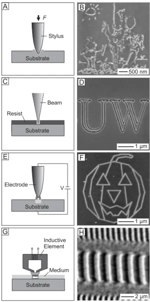
Figure 2.Simplified schematic (left panel) and representative examples
(right panel) of four different techniques that write patterns without any ink. A) A rigid stylus is used to induce the indentation, deformation, or displacement of material on a surface. B) The AFM topographic image of Pablo Picasso's ªDon Quixoteº that was carved in the surface of a poly-carbonate film with an AFM tip (courtesy of Asylum Research, Santa Bar-bara, CA). C) A focused beam of photons, electrons, or other energetic particles is used to induce changes in a resist material. D) SEM image showing the letters ªUWº that were written with an electron beam in a thin film of PMMA (courtesy of G. Golden, Center of Nanotechnology at the University of Washington). E) An auxiliary electrode is used to apply an electrical field to the substrate in a localized fashion. F) AFM image of a cartoon feature generated by anodically oxidizing the silicon surface with a conductive, scanning probe (courtesy of B. Wallace, P. Harris, and K. Jones, Veeco Metrology Group, Santa Barbara, CA). G) An inductive element on a recording head is used to generate domains with uniform magnetization directions in a thin layer of ferromagnetic material. H) Magnetic force microscopy image of the magnetization pattern of a recorded track on a hard disc (reproduced from [41c] with permission, copyright 1999, Annual Reviews).
mechanism, by which species present on the surface (or some-times in the bulk) of a substrate undergo changes (often irre-versible) in a spatially confined manner. In practice, such changes can be induced by a mechanical, physical, optical, electrical, chemical, or magnetic means, or a combination of them; and they are often derived from a complex set of processes that may involve both energy conversion and/or chemical reactions. Towards the end of this section, we briefly discuss three writing techniques (Fig. 3) that are based on localized add-on of materials from an external source or reser-voir.
2.1.1. Writing with a Rigid Stylus
This writing scheme involves the mechanical displacement or modification of a material on the surface of a substrate in a spatially controlled way (Fig. 2A). It is also known as micro-machining.[9]The process generally requires a direct contact between the surface of a substrate and a rigid stylus that is moved across the surface to engrave a pattern in relief. In any mechanical writing process, the durability of the stylus and thus the degradation of edge resolution with time are two ma-jor issues that need to be considered, since high loading forces might be involved. The selection of an appropriate stylus depends on the application of the resultant pattern. A macro-scopic stylus is mainly used for the machining of bulk
materi-als in an effort to engrave relief patterns with less stringent re-quirements for edge resolution and feature size. The writing of high-resolution patterns is often accomplished by scanning probe techniques including both scanning tunneling microsco-py (STM) and atomic force microscomicrosco-py (AFM), which employ ultrasharp tips.[10] The resolution that can be obtained with these techniques can vary from 0.1 nm (corresponding to the size of an individual atom) to the micrometer-sized scale (involving large ensembles of atoms or molecules). Scraping, ploughing, or indentation with a scanning probe has been demonstrated for a rich variety of materials that includes polymers (Fig. 2B),[11]metals or oxides,[12]and self-assembled monolayers (SAMs).[13]For a relatively thick film, this process usually results in the formation of holes or trenches that are surrounded by walls consisting of the displaced material. The probe tip can also be used to grab weakly adsorbed molecules or small particles from a surface, and transfer them to another region of the same substrate to generate highly ordered struc-tures.[14] However, this strategy seems to be less frequently used than the former one because the grabbing, moving, and unloading steps can be slow and hard to control.
2.1.2. Writing with a Beam of Photons or Other Energetic Particles
These approaches share the same operational principle, in which the spot of a tightly focused beam is scanned across the surface of a susceptible material (Fig. 2C). The dissipation of beam energy can proceed in a number of different ways and may include various types of physical and chemical processes, depending on the type of radiation, its dose, and the materials that are involved. Generally, the patterning process can be additive, involving the deposition of species in or close to the illuminated spot (see Sec. 2.1.5.), or subtractive, due to the removal of material from the surface of a substrate. In addi-tion, such a process may consist of physical or chemical reac-tions that only lead to the formation of a latent image in the medium.
Focused laser beams have been adapted for a number of different fabrication schemes. The laser-assisted ablative micropatterning of a solid surface relies on the removal of a material by species such as radicals that are formed in the photochemically excited gas.[15]This technique can be applied to a variety of inorganic materials in a localized, well-con-trolled manner, whereas the removal of polymers generally requires the use of specially designed laser ablation resists that perform with high adsorption coefficients, exothermic decomposition at specific positions of the polymer chains, and formation of gaseous products.[16] Commercial photomasks are often fabricated using this technique when the feature sizes are larger than 1±2lm. Alternatively, materials can be deformed, melted, or otherwise modified at the focal spot due to thermal energy dumped by the laser beam.[17]Lithography based on near-field scanning optical microscopy (NSOM) uses a transparent, aluminum-coated probe tip at the end of an
REVIEWS
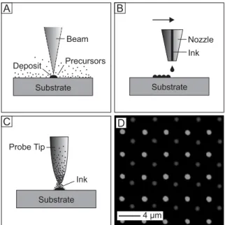
Figure 3.Illustration of three different writing schemes that use add-on
processes. A) Precursor molecules are decomposed in or close to the fo-cal point of a beam to deposit a material on the surface of a solid sup-port. B) Inkjet printing, where liquid-like ink is ejected from a nozzle and dispensed onto a substrate in a controlled way. C) Writing of ink with a pen, which may also involve the use of a liquid layer to mediate the ink transport from the pen to the substrate. D) A fluorescence microscopy image of an array that contains two different types of fluorescence-la-beled, hybridized DNA sequences generated by dip-pen nanolithography (reproduced from [60d] with permission, copyright 2002, American Asso-ciation for the Advancement of Science).
optical fiber that functions as a waveguide to direct light from a laser source onto the surface of a substrate.[18]When the tip is sufficiently close to the substrate, the exposure can be lim-ited to an area that is substantially smaller than the diffraction limit in the far-field. This technique has been used to selec-tively polymerize conventional photoresists;[19]to induce the activation or sensitization of reactive species;[20]and to loca-lize melting, evaporation or photo-oxidation processes.[21]
Focused beams of energetic particles comprising electrons, ions, and electrically neutral metastable atoms provide other means for generating patterns in a proper resist material.[22±24] These techniques have extremely high resolution capabilities because of their short wavelengths (< 0.1 nm) combined with a large depth of focus. Electron-beam (e-beam) lithography is a feature that can be readily added to most conventional scan-ning electron microscopy (SEM) systems. Although high throughput continues to be a major challenge of this tech-nique, e-beam lithography has become a standard tool for writing arbitrary patterns for many technological and scientif-ic applscientif-ications. A variety of materials have been demonstrated for use with e-beam lithography, including polymers (Fig. 2D),[25] inorganic materials,[26] and SAMs.[27] Reactions that are thereby induced depend on the chemical composition of a resist. For polymers, they can include polymerization, crosslinking, local chain scission, or a more complex process such as chemical amplification involving acids or bases.[7f,28] The practical resolution of this technique is mainly deter-mined by the spot size of the beam, and several other factors such as scattering effects and the generation of secondary electrons. Poly(methyl methacrylate) (PMMA) remains a classical resist for e-beam lithography, and much work con-tinues to be done with this polymer despite extensive techno-logical advances and development in e-beam lithography, and the large number of resist formulations that have been devel-oped. Direct etching induced by an e-beam is possible, but generally requires higher doses, which limits its practical utili-zation.
Techniques using focused ion beams (FIBs) are concep-tually related to e-beam lithography. In principle, the higher mass of ions may result in patterning capabilities that are less prone to distortions due to back-scattering from the substrate. Other advantages include the possibility of highly localized implantation doping (the formation of a new material or a new phase under the surface of a substrate), ion-induced de-position, and the capability of removing material from a sur-face using ion milling or ion-beam assisted etching. Up till now, high-resolution variants of these techniques remain in a relatively less-developed state than e-beam writing.
2.1.3. Writing with an Electrical Field
In an electrical writing process, the surface is locally modi-fied using an electrical field or current.[29]An auxiliary elec-trode is thereby moved in a predefined path above a (conduc-tive) surface, which serves as a working electrode (Fig. 2E).
The electromagnetic field that is applied can induce a variety of physicochemical changes to the species (atoms, ions, or molecules) that are present at the interface. The outcome depends on the properties of the species, as well as the condi-tions under which the experiment is performed. It can be derived either from the field itself (charging), as a conse-quence of increased current flow (Ohmic heating), or because of redox reactions occurring at the tip or on the surface of the sample. The patterning methodology and the experimental conditions can also vary substantiallyÐwhile the STM-based manipulation of individual atoms is commonly performed under ultrahigh vacuum conditions and at cryogenic tempera-tures, scanning electrochemical microscopy (SECM) with electroactive species often requires the presence of solvents or reactants, sometimes at elevated temperatures. In general, SECM yields larger feature sizes than other scanning probe techniques, and has been used for electrochemically induced desorption of alkanethiol SAMs on gold and selective deposi-tion of metal islands on solid surfaces.[30] Conventional scanning probe techniques including both STM and AFM have also been adapted for a number of demonstrations. Typi-cal field-assisted transfer processes involve the loTypi-calized posi-tioning of metal clusters,[31]creation of pits or holes,[32] and manipulation of individual molecules or atoms.[33]Direct elec-trochemical processes include the oxidation of silicon (Fig. 2F)[34]or other solid materials,[35]and modification of re-sist films,[36]functionalized silanes,[37]alkanethiolate SAMs,[38] or other organic thin films.[39]Scanning probe techniques have also been demonstrated for writing nanostructures (e.g., mag-netic nanoparticles) on solid supports in conjunction with a chemical decomposition process.[40]
2.1.4. Writing with a Magnetic Field
Magnetic writing (and reading) is central to information storage technology.[41]In this application, the writing element is an inductive device on a recording head, which is used to magnetize small areas of a magnetic medium (e.g., iron oxide particles, or a polycrystalline alloy composed of Co, Cr, and Pt) supported on a tape or hard disc (Figs. 2G,H). This way, bits are generated in the form of magnetization patterns that can encode certain types of signals. The most attractive fea-ture associated with a magnetic writing process is that only physical changes are involved in the formation of patterns, and the changes are usually reversible. The read-back of the recorded signal is the reverse process, and can be achieved using a magneto-resistive sensor hosted on the same head. Most magnetic media exhibit in-plane magnetization, but some (multilayered) films can also be magnetized perpendicu-lar to the surface. The lateral density of bits that can be writ-ten on a hard disk drive has increased substantially over past several decades, primarily by making the read±write head smaller, decreasing the grain size and the thickness of the recording media while increasing its coercivity, and by reduc-ing the distance between the head and the medium durreduc-ing
operation.[42] The composition and morphology of the mag-netic medium are essential since noise effects can occur when magnetized grains couple with each other, and domain walls fail to nucleate or move after magnetization.
The use of magnetic particles with smaller grain sizes is essential in improving the writing density. But the reduction in grain size might, however, be constrained by superpara-magnetismÐan effect in which grains cannot retain the induced magnetization owing to thermal agitation when they become too small.[43]Current approaches to overcome these limitations include the introduction of a nonmagnetic phase at grain boundaries,[44] and the transition to patterned (or dis-crete) media using arrays of single domain particles.[45]In the latter approach, bits are defined by physical objects, not by the boundary between two oppositely magnetized regions in a thin film. Despite the various challenges associated with fabri-cation of such devices, objects with lateral dimensions of a few nanometers could potentially support information storage densities of 150 Gbit cm±2and beyond.[45]
2.1.5. Writing by an Add-On Process
Add-on writing (Fig. 3) is attractive when one needs to pat-tern a material that is incompatible with the resist, image development, or etching process. In addition, a direct add-on process can provide excellent control over the surface chemis-try of a substrate, and allows for the fabrication of systems with high chemical/functional complexity without severe cross-contamination. From the economical point of view, an add-on process also helps to reduce the number of processing steps, to minimize the waste of raw materials, and to save energy.
Laser-induced chemical vapor deposition (LCVD) has been widely explored as a method for patterning solid substrates, since it is a fast and reliable way to deposit a variety of materi-als on both planar and nonplanar surfaces (Fig. 3A).[46]The writing can be carried out in two major variantsÐphotolytic decomposition, where photon adsorption is accompanied by cleavage of chemical bonds, or pyrolytic decomposition, where heating thermally dissects the precursor compound. Gaseous precursors such as alkyl or carbonyl metal com-pounds are often used, which must adsorb on the surface of a substrate before or during the exposure. Laser-assisted de-position of metal complexes from the solution phase,[47] laser-enhanced electro- and electroless plating,[48] and photother-mal decomposition of metal-doped polymer thin films have also been demonstrated.[49] The quality of the final product can vary from isolated crystallites to continuous films. The smallest feature size is generally limited by the spot size of the beam: while critical dimensions on the order of 500 nm have been routinely obtained with regular laser beams, better reso-lution is achievable with the use of NSOM-based lithography, which has already been shown in conjunction with chemical vapor deposition (CVD) for a variety of materials.[50]In addi-tion to lasers, focused beams of electrons and ions can also be
applied to locally deposit various types of materials onto the surface of a solid substrate from a gaseous precursor.[51]As a matter of fact, FIB-based deposition represents one of the best-established, most commonly used techniques for repair-ing the defects on photomasks or integrated circuits.
Inkjet printing (IJP) has recently emerged as an attractive technique for depositing minute quantities of material on sur-faces with good spatial control (Fig. 3B).[52]In this technique, small volumes of liquid ink from a reservoir are ejected through a nozzle and dispensed onto the substrate. Two modes of operation exist, in which the liquid is either pumped through the nozzle to form a continuous jet of liquid, or in which small droplets are generated by applying an acoustic or thermal pulse. IJP has a range of advantageous attributes, and some of them are particularly relevant when reel-to-reel manufacturing of patterns on flexible substrates is desired: i) it is a contact-free technique; ii) it is capable of providing high throughput, in particular when a large number of nozzles are used in parallel; iii) it allows the simultaneous printing of different materials delivered from multiple nozzles, and iv) it provides good alignment capabilities and a precise control over the volume of deposited materials. Nozzles used for IJP typically have a diameter of 20±30lm yielding drop sizes in the range of 10 to 20 pL. Statistical variations of the flight direction of droplets and their spreading on the substrate both limit the resolution of IJP, which is currently in the range of 20±50lm. IJP has already become a method of choice for generating polymer features,[53]and may also have the poten-tial for patterning other materials such as ceramic powders, metal precursors, and colloids on a number of different sub-strates (both rigid and flexible). Another interesting applica-tion for IJP that has been actively explored is related to the fabrication of biochips.[54]
Dip-pen nanolithography (DPN) has been demonstrated as a high-resolution technique for writing liquid-based ink on substrates.[55] In this technique, the ink is loaded onto an AFM tip, and delivered to the surface of a substrate via a thin water meniscus that forms between the tip and the substrate, thereby serving as a medium for ink transport with nanometer dimensions (Fig. 3C). DPN (and its variants) has already been successfully applied to pattern a broad range of materials including alkanethiol monolayers on gold,[56] colloidal parti-cles or sols,[57]inorganic metal salts,[58]polymers,[59] and bio-molecules such as proteins and DNA (Fig. 3D) on a variety of substrates.[60]The latter example is particularly interesting as it might provide a rational scheme for fabricating gene and proteomic chips for applications in life sciences and health-care.
2.2. Self-Assembly
The concept of self-assembly provides a unique and ex-tremely interesting route towards the formation of patterned structures via a bottom±up approach.[61]A system will self-as-semble if its constituents (or building blocks) have
ate interaction capabilities to aggregate into a stable, well-de-fined structure that can range from a few nanometers to milli-meters in size. A self-assembly process can be readily con-trolled by tailoring the properties of the building blocks, which include, for example, their topography, shape, surface functionality, and electrical potentials.[62]The final structure is reached by equilibrating to the lowest free-energy state, in which both attraction and repulsion between the building blocks are well-balanced. Self-assembly has been beautifully demonstrated in biological systems to build complex, well-controlled structures. The folding of polypeptide chains into functional proteins, and the formation of dynamic cell mem-branes from phospholipids are just two appealing examples.[63] Inspired by the importance of self-assembly in nature, scien-tists have demonstrated a range of concepts to explore and use self-assembly as a synthetic tool for generating highly or-dered arrays of structures.
In general, the building blocks can be divided into three categories depending on their length scales: The first one, molecular self-assembly, uses the interaction between mole-cules based on electrostatic, hydrophobic, or van der Waals' interactions, as well as hydrogen bridges or metal-ligand bonds.[64] The formation of crystals, nanocrystallites, SAMs, lipid bilayers, micelles, and phase-separated block copolymers (see below) all belong to this category. The second category involves the assembly of nanoscale objects such as colloidal particles, nanowires, nanotubes, and related structures, form-ing ordered arrays or lattices,[65]while the third uses objects with meso- to macroscale dimensions.[66]Assembly of objects for the last two categories may differ from that of molecules because one needs to rely on gravitational force, external electromagnetic fields, physical confinement, and magnetic, capillary, or entropic interactions to direct the assembly pro-cess. The resulting structures can even be controlled by vary-ing the interactions between objects with appropriate features on their surfaces. Examples for the last two categories include fluidic self-assembly,[67]which is mainly based on shape recog-nition; the solder-based assembly of objects using the surface tension of molten solder drops,[68]the alignment and crystalli-zation of particles in ferrofluidics based on magnetic self-as-sembly;[69] and template-assisted self-assembly,[70] in which spherical colloids can be organized into well-defined aggre-gates through the application of physical confinement. As we are limited by space, we only discuss two examples involving molecular and mesoscale self-assembly, which may have inter-esting implications for the formation of patterned 2D nano-structures.
2.2.1. Phase-Separated Block Copolymers
Block copolymers (BCs) consist of at least two chemically distinct, immiscible polymer fragments that are joined by a covalent bond.[71]These systems can develop a variety of reg-ular domain patterns at equilibrium. The size and the period of the structures both depend on the conditions of preparation
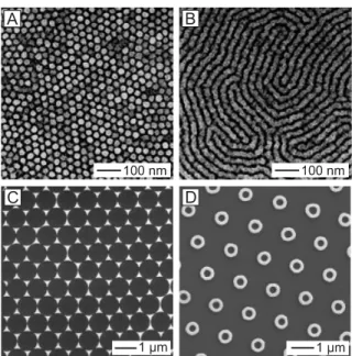
as well as on the relative chain lengths of the participating polymers, and are typically on the order of 10 to 100 nm.[72] Often, the polymer fragments show chemical or physical dis-similarities that allow the selective removal of one component leaving a porous array behind on the substrate, which can be used as a mask for lithographic applications. This approach has been shown in conjunction with reactive-ion etching (RIE) to produce high-density arrays of nanometer-sized structures on substrates (Figs. 4A,B).[73]It is equally possible to fabricate arrays of dots and nanocrystals of other materials using template-directed growth or deposition.[74]
Alterna-tively, BCs can act as templates to disperse particles into or-dered arrays due to the preferential adsorption on domains of one component in the polymer matrix.[75]One of the major is-sues is the control of domain orientation to produce highly or-dered, single domain structures over large areas. Two strate-gies are currently being pursued for solving this problem: placing the BCs in a strong electrical field to improve spatial ordering,[76] and depositing the BCs on surfaces patterned with different functional groups to induce long-range order-ing.[77]By adding more blocks to the traditional diblock sys-tem, it is also possible to generate complex 3D structures that are difficult to fabricate using conventional microfabrication techniques.[78]
Figure 4.Examples of patterns that were fabricated using self-assembly
methods. A,B) Scanning electron micrographs of two different types of patterns that were generated in silicon nitride by using phase-separated polystyrene±polybutadiene diblock copolymer films as the masks for re-active-ion etching (reproduced from [73] with permission, copyright 1997, American Association for the Advancement of Science). C) Scan-ning electron micrograph showing a 2D array of triangular gold islands that were produced by evaporation through the voids in a monolayer of spherical colloids self-assembled on a silicon substrate. D) Scanning electron micrograph of gold rings that were fabricated by spreading an alkanethiol ink from the edges of silica beads that had been assembled on a gold substrate, followed by lift-off of the beads and etching the gold selectively.
2.2.2. Nanosphere Lithography
Nanosphere lithography (NSL) uses monodispersed spheri-cal colloids that are first assembled on a flat surface to form a close-packed monolayer with a hexagonal symmetry. The monolayer then serves as a physical mask for subsequent pro-cessing steps.[79]In most demonstrations, a metal is evaporat-ed through the monolayer to fill the void spaces among adja-cent colloids in the monolayer lattice. Upon removal of the colloids by lift-off, a periodic array of nanometer-sized, pyra-midal islands of the metal is left behind on the substrate.[80] The lateral dimensions of these islands and the separation between them can both be controlled by varying the diameter of the spherical colloids, while the vertical dimension mainly depends on the amount of material that is deposited. When a monolayer lattice of spheres is used and the sample is placed normal to the deposition direction, islands with triangular shape are obtained (Fig. 4C). By changing the tilt angle of the substrate with respect to the deposition direction, a number of other geometries, in which features are either overlapped or separated by a small gap have been observed.[81]When a dou-ble layer of spheres is used, circular dots corresponding to the small openings that remain in a closely packed lattice are formed.[80] Most recently, an array of spherical colloids was also used to guide the spreading of a liquid-like ink on a sub-strate and to form ring-type structures.[82]In a typical process, an alkanethiol ink was applied to silica beads (supported on a gold or silver substrate) using a planar PDMS stamp. The cir-cular footprints of the beads were outlined by the thiol mole-cules resulting in the formation of ring structures that could be revealed after lift-off of the beads, followed by wet-chemi-cal etching (Fig. 4D). Although large areas can be patterned in parallel by NSL, this technique remains sensitive to defects, distortions, and domain boundaries that naturally appear when spherical colloids are crystallized on a solid support. The patterns that can be generated using this approach are very limited in terms of design and complexity.
3. Replication of Patterns
The purpose of pattern replication is to reproduce (or dupli-cate) the structural information on the surface of a mask or master using a different material in a single step, rapidly, and with high fidelity. The task of replication can be divided into three categories depending on the element that carries the pattern. In the first category, a patterned mask is used to mod-ulate a flux of either electromagnetic radiation or physical matter moving towards the surface of a substrate. This is usually achieved by interposing the mask between the sub-strate and the exposure source, from which a flux of radiation or matter is emitted. The second category is based on the use of a master, against which patterns are duplicated using var-ious forms of replication such as molding, embossing (imprint-ing), and printing. The last category covers techniques in which only the edges of a structure are reproduced or
trans-ferred. Collectively known as edge lithography, these tech-niques are becoming increasingly useful because they enable the fabrication of a rich variety of simple but very small struc-tures efficiently and inexpensively.
3.1. Duplication with a Mask
Essentially all versions of photolithography belong to this category. The key component is a photomask that consists of alternating regions of opaque and transparent features to modulate the intensity of light impinged on a photoresist film. The photomasks are usually fabricated on rigid substrates such as quartz. Flexible substrates (e.g., transparency films) can also be used when the features are relatively large (> 50lm) and no registration between the features is required. Add-on processes that involve the use of stencil or lift-off masks are also part of the masked duplication ap-proach. In these cases, the mask can also be fabricated in situ on the surface of a substrate using various patterning tech-niques such as nanosphere lithography (Sec. 2.2.2.), photoli-thography (Sec. 3.1.2.), and soft liphotoli-thography (Sec. 3.2.).
3.1.1. Masked Exposure to Photons
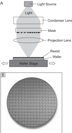
This technology is widely known as photolithography or optical lithography.[1,6]It has been the mainstream technology for high-volume manufacturing in the semiconductor industry for the past several decades, and this trend is expected to con-tinue for the foreseeable future. Optical lithography can be carried out in three different modes, in which the mask is either in physical contact with the resist film (contact print-ing), very close to the resist film (proximity printprint-ing), or further away to project the pattern onto the resist film (pro-jection lithography). Contact-mode photolithography is most commonly used in the setting of a research laboratory. It is not well-suited for fabrication tasks that demand high throughput, accuracy, and resolution because: i) the physical contact can cause contamination and damage to the mask; ii) the features on the mask are replicated at a 1:1 ratio and must therefore be as small as those desired to be generated in the resist; and iii) it is difficult to achieve accurate registration due to the lateral shift between mask and substrate during the contact process. Optical lithography in the proximity mode overcomes some of these drawbacks but it remains inherently limited to the 1:1 reproduction scheme. In projection photo-lithography, an interposed lens system demagnifies the fea-tures on a photomask (usually by a factor of four) and pro-jects the image onto a resist film. With this configuration, the structures generated in the resist are smaller than those pres-ent on the mask. Since the mask and the resist film are sepa-rated from each other, alignment and registration can be ac-complished conveniently and accurately. For these technical reasons, fabrication lines in the semiconductor industry are all built upon this approach using a step-and-repeat lithographic
tool that is called a stepper (Fig. 5A). Such a tool is especially well-suited for accomplishing superb uniformity, accuracy, and resolution over the entire wafer (Fig. 5B).
As restricted by optical diffraction, it is necessary for pro-jection-mode lithography to continuously shorten the wave-length of the light source in order to keep pace with the trend in downsizing the feature size. However, the transition of a lithographical process to shorter wavelengths is by no means straightforward, and always imposes relentless technical chal-lenges that include the availability of light sources, lens mate-rials, coatings, and masks. It is also crucial to have resist sys-tems that perform well at the wavelength that is to be utilized, as well as the ability to achieve overlay accuracy and to mini-mize the contamination of surfaces.
In addition to their use as a powerful tool to generate struc-tures in photoresist films, optical lithography has also been adapted to fabricate and manufacture biochips.[83]In this case, light exposure is used to induce photochemical reactions at specific sites of molecules supported on a solid substrate. By repeating the reactions with different chemical reagents and appropriate masking, it is possible to construct molecular
chains on the same solid support with essentially all combina-tions of chemical composicombina-tions (e.g., RNA chains having dif-ferent numbers of base pairs and difdif-ferent sequences). In related studies, exposure to photons through a mask has also been explored to modify the interfacial properties of a solid substrate.[84]
3.1.2. Masked Etching or Deposition
This approach, which is sometimes referred to as dry lift-off, involves the use of a shadow or stencil mask that contains void regions to direct the etching or deposition process (Fig. 6A).[85]Typically, such a mask is made of a rigid materi-al, and the void features are simple and discrete because the
freestanding mask needs to be continuous and mechanically robust. The formation of complex and connected features therefore requires multiple, sequential processing steps by either translating the same mask laterally or using masks with complementary designs, as well as by appropriate alignment of the features with respect to each other. When materials such as silicon nitride, glass, or highly ordered porous anodic alumina are used, high-resolution stencil masks with feature sizes as small as 20 nm have been demonstrated.[86] Polymer-based materials are useful when uneven or curved substrates are involved.
Masked deposition can be readily applied to a broad range of vaporizable materials that include metals (Fig. 6B), semi-conductors, dielectrics, and organic compounds.[85]
Angle-de-Figure 5.A) Simplified schematic of the optical system in a stepper. The
demagnified image of a mask is projected onto the surface of a resist film, and the movable stage allows this process to be repeated at other locations on the same wafer. B) Photograph of a 12 in. wafer containing an array of Pentium IV Processors fabricated using Intel's 130 nm pro-cess technology (courtesy of Intel Corporation, Santa Clara, CA).
Figure 6.A) Schematic of masked deposition and etching. B) Scanning
electron micrograph of gold features formed on the surface of a glass capillary (~1 mm in diameter) by evaporation through a polymeric mask, followed by removal of the mask (reproduced from [88a] with permission, copyright 1996, American Chemical Society). C) Scanning electron mi-crograph of features anisotropically etched in a Si(100) wafer with pat-terned gold layer as the mask, which still remained on the surface (repro-duced from [91a]).
pendent deposition has also been used to spatially control the placement of materials at the bottom of the mask, which is attractive for the introduction of gradients or the deposition of different materials in close proximity.[87]Similar to contact-mode photolithography, a small gap remains when a rigid mask is placed on a solid substrate, which might cause en-largement of features due to lateral diffusion. In addition, rig-id masks are less practical for deposition from solution phase. This limitation can be overcome by using an elastomeric material to fabricate the mask, which can seal the substrate reversibly via conformal contact.[88]
In the case of masked etching, the mask serves as a physical barrier to alter the exposure of a substrate to reactive etchants or atom bombardment.[24,89]The etching process can be isotro-pic or anisotroisotro-pic depending on the crystallinity and crystallo-graphic orientation of the substrate. In most cases, the pat-terned features in the mask can be faithfully transferred into the underlying substrate with variable vertical dimensions. When wet etching is applied to single crystal wafers with specific orientations, the resultant structures usually exhibit tapered profiles (Fig. 6C) due to the anisotropy in etch rate for different crystallographic planes.[90] Undercutting is another issue that needs to be addressed in order to obtain patterned relief structures with well-controlled dimensions. In general, undercutting is less severe for a gas phase etching process.
3.2. Replication with a Master
A replication process can generate patterns either identical or complementary to those on the master depending on the detailed procedure (Fig. 7). Some of these replication meth-ods are referred to as soft lithographic techniques because they rely on the use of an elastomer, usually poly(dimethyl siloxane) (PDMS), as the key material to fabricate masters in an effort to achieve intimate, conformal contact with flat or curved substrates over relatively large areas.[91]Soft lithogra-phy offers immediate advantages in applications where photo-lithography and other conventional microfabrication tech-niques are ineffective. Examples include the patterning of curved substrates, the use of materials that are incompatible with photoresists or developers, and large-area fabrication where the cost is a major concern. The use of an elastomeric master also allows modification of the test pattern and feature size by deforming the master mechanically. This section will cover both rigid and soft masters, with a focus on the latter one because of its versatility and surging popularity.
3.2.1. Embossing with a Rigid Master
Embossing (or imprinting) is a simple and convenient tech-nique that generates relief patterns in a polymer by mechani-cal deformation using a rigid master (Figs. 7A,B).[92]The poly-mer must be either thermoplastic, UV- or thermally curable,
REVIEWS
Figure 7.Schematic (left panel) and examples (right panel) of replication
techniques that rely on the use of masters. A) Embossing that uses a rig-id master to imprint into a deformable material under mechanical force. B) SEM image of parallel lines generated in PMMA film by embossing with a rigid master (reproduced from [92h] with permission, copyright 2001, the Materials Research Society). C) Replica molding by which a liq-uid prepolymer is cast on a mold and then cured into a solid. D) SEM image of polyurethane microstructures fabricated by replica molding against a PDMS mold. E) Microcontact printing, where a stamp is used to define a pattern of ink on a substrate. F) SEM image of silver patterns generated by microcontact printing with a thiol ink, followed by selective chemical etching of the unprotected regions. G) Microfluidic patterning, where the channels of a microfluidic network are used to deliver reac-tants from a reservoir to the surface of a substrate with spatial control. H) A fluorescence microscopy image of fluorescence-labeled proteins that were deposited on a PDMS substrate from a set of parallel channels in a silicon mold (reproduced from [125i] with permission, copyright 2001, American Chemical Society).
or otherwise deformable to adapt the shape of the patterns on the master. In the case of a thermoplastic material such as PMMA, the substrate is heated above its glass-transition tem-perature (Tg) during imprinting, and then cooled below Tg before it is separated from the master. For this reason, this process has been referred to as hot embossing. When the polymer is a UV- or thermally curable material, it is imprinted in its liquid state, and then hardened into patterned structures through a UV- or thermal-curing process. In most cases, resid-ual films of the polymer remain in the compressed areas, which can be removed using a dry etching process. Exceptions were found when the residual film became sufficiently thin to dewet from the substrate.[93]The resolution of structures that can be generated using this technique is mainly determined by the mechanical stability of the master, the properties of the polymer (including wetting, adhesion, and viscosity), and the dimensional changes of the imprinted structures with temper-ature or pressure. Experimental results indicate that fetemper-atures with critical dimensions well below 10 nm are achievable without modifying the procedure significantly. In a new var-iant of this technique, laser-assisted direct imprinting, silicon was directly patterned by using a laser to induce the silicon substrate to melt at its top surface.[94]In general, it is non-tri-vial to separate a rigid master from a rigid substrate without causing damages to the fine structures on their surfaces.
3.2.2. Molding with an Elastomeric Master
In a molding process, structures are formed inside the void spaces of a master or mold (Fig. 7C).[95]With the use of an appropriate material, the shape, structure, and pattern of the mold can all be transferred into the replica with high fidelity and accuracy, even on the nanometer length scale. This tech-nique also allows the duplication of 3D structures in a single stepÐsomething that cannot be easily achieved using other techniques. Molding can be carried out in a variety of ways, depending on the composition of the mold, the steps that might be part of the process, and the materials that are in-volved. Here we only focus on a number of attractive variants. Replica molding (REM) of organic polymers against an elas-tomeric PDMS mold (Fig. 7D) can be performed with superb fidelity.[96] The use of an elastomeric mold ensures easy release of the replica, and provides the unique opportunity to modify the size and shape of the relief structures by mechani-cal or thermal deformation. Feature sizes below 2 nm have been reported for replicas in PMMA, PDMS, and polyure-thane (PU).[97]Microtransfer molding (lTM) is a procedure that requires at least three steps to complete:[98]i) the voids on an elastomeric mold are filled with a polymer precursor; ii) the excess material is removed; and iii) the mold is placed on the desired substrate. After curing the prepolymer, the mold is peeled off leaving behind the replicated structures on the substrate. An important advantage oflTM is its capability to generate complex patterns in a layer-by-layer fashion and on non-planar or curved surfaces, which often is a prerequisite
for building 3D microstructures. In another variant, solvent-assisted micromolding (SAMIM),[99]a solvent is used to soft-en a polymeric material so that it can adapt the shape of a PDMS mold. As the solvent dissipates and/or evaporates, the polymer hardens, preserving a pattern complementary to that of the mold. SAMIM has been successfully applied to a vari-ety of polymers including Novolac-based photoresists, cellu-lose acetate, and conducting polymers.[100]The only require-ment seems to be that a suitable solvent is available for the desired polymer. Micromolding in capillaries (MIMIC) repre-sents a fourth variant that forms complex structures on solid substrates by molding against an elastomeric master.[88a,101]In this method, a PDMS mold is used to define a network of con-nected channels when it comes in contact with a solid surface. Liquids placed at the open ends of the network will sponta-neously fill the channels as a result of capillary forces. During the filling process, material can be transported, which might either be hardened by a curing process, or deposited from so-lution onto the substrate. Microchannel systems are generally limited to the fabrication of relatively simple and continuous structures, but allow for patterning multiple materials in par-allel. MIMIC has been shown for a broad range of materials including polymers (and prepolymers),[102]sol±gel precursors to ceramic materials,[103]and spherical colloids.[104]
3.2.3. Printing with an Elastomeric Stamp
Printing involves the use of a stamp to transfer patterned ink onto a substrate in a simple and convenient way (Fig. 7E). It is an inherently additive process. Five different printing schemes exist, which all rely on contact between the stamp and the substrate:[91c] i) relief printing, ii) intaglio printing, iii) lithographic printing, iv) screen-printing, and v) xerogra-phy. Here we mainly focus on relief printing, with some brief discussions on lithographic printing and xerography. We do not cover intaglio and screen-printing because the basic prin-ciples of these two techniques are closely related to molding and masked deposition, respectively, which have already been discussed in the previous sections. Relief printing includes both letterpress printing and flexographic techniques, in which a pattern is transferred from the raised regions of a stamp. Microcontact printing (lCP) belongs to this category, and relies on the use of a PDMS stamp.[105]In a typical proce-dure, the stamp is first inked by covering the patterned face with a solution of ink, dried, and then brought into contact with the surface of a substrate. Microcontact printing was first demonstrated for SAMs of alkanethiols on gold, which is probably still the most studied and best-established system for this technique.[105]There are several reasons for the success of this particular system:[106] i) alkanethiols rapidly chemisorb onto a gold surface via the thiol group; ii) the absorbed spe-cies self-organize into a dense and highly ordered monolayer as driven by the strong van der Waals' interactions between the long alkyl chains; and iii) the self-limiting, autophobic nature of the forming monolayer helps confine it to the
regions of contact. The same protocol also works for alka-nethiolate SAMs on other metals (Fig. 7F),[107±109]as well as for alkylsiloxanes on hydroxyl-terminated substrates,[110]and alkylphosphonic acids on aluminum oxide.[111]Other interest-ing examples include the direct printinterest-ing of chemical species such as catalysts or catalytic precursors,[112] colloidal parti-cles,[113] dendrimers,[114] organic reactants,[115] conventional polymers,[116]lipid bilayers,[117]and proteins.[118]In addition to liquid-based inks, a thin, evaporated film of metal (e.g., gold or aluminum) can also be readily transferred onto the surface of a substrate using a variant of this technique termed nano-transfer printing (nTP).[119] Feature sizes ranging from 350 nm to several millimeters can be routinely achieved using lCP, whereas patterning of smaller structures (in par-ticular those that have critical dimensions below 100 nm) still remains a grand challenge. The use of more dedicated polymer formulations and fabrication of stamps from com-posite materials were important improvements on the way to extending this technique into the sub-100 nm range.[120] Dif-ferent from photolithography, lCP can be readily extended to generate patterned features on curved substrates with sub-micrometer resolution.[121]Lithography printing involves the use of a flat, chemically patterned stamp comprising areas that either accept or repel the ink.[122]This concept is of cru-cial importance in the paper printing industry, but has not been frequently used for micropatterning. Xerography diverges from the above printing techniques since the images are created by either charging or discharging selected regions on a substrate during contact.[123] The attraction of toner powders in a commercial printer or copier relies on this pro-cess, for example. Patterns in a magnetic medium have also been generated by printing with stamps that contain magnetic features.[124]
3.2.4. Microfluidic Patterning
Microfluidic patterning relies on the manipulation of liquid flow in channels of microfluidic networks (lFNs) that have di-mensions in the range of 1 to 100lm.[125] This technique shares some operational principles with MIMIC (Sec. 3.2.2.), but usually does not involve any molding process in the com-mon sense. The liquid serves essentially as a transport and re-action medium that can be used either to deposit minute amounts of a material on a substrate (Figs. 7G,H), or to re-move species from a surface by dissolution. Depending on the application, there can be many types of microfluidic devices, and each one of them might contain components for injection, separation, detection, mixing, and heating, among others. Al-though capillary action largely dominates the motion of a liq-uid in a microchannel, external actuators or pumps are often necessary to mediate the liquid flow, especially over long dis-tances. Microfluidic patterning is particularly attractive for biochemistry and cell biology, where binding and recognition events between species of interest can be localized in a rela-tively simple and convenient manner.
3.3. Edge Lithography
Edge lithography comprises an ensemble of techniques, in which the edges of a structure become the features of the resulting pattern. These approaches contribute to size reduc-tion, and have emerged as attractive tools, in particular when high-resolution lines (wires or trenches) and related structures are the fabrication targets. One of these techniques, near-field phase-shifting photolithography,[126]derives from the conven-tional setup for contact-mode lithography, but uses a confor-mal mask (made of an elastomer such as PDMS) to achieve a better contact with the resist film. The relief structures on the mask, although entirely transparent, can induce changes in the phase of light used for exposure, and lead to largely unex-posed or over-exunex-posed regions at the edges due to destructive/ constructive interference. By using light with a wavelength of 248 nm, this technique allows, for example, lines as narrow as 50 nm to be fabricated in a positive-tone resist. In addition to straight lines, this technique has been used to generate other simple patterns such as dots and rings of various geometries (Fig. 8A). In topographically directed photolithography (TOP),[127]features on the surface of a photoresist film (fabri-cated by SAMIM or embossing) serve as optical elements to
disperse and phase-shift incident UV light inside the resist layer during exposure. Upon development, complex struc-tures and patterns can be yielded with feature sizes ranging from 50 to 200 nm over relatively large areas. In a third approach, called controlled undercutting,[128]the edges of a resist pattern are transferred into the underlying metal film. This approach includes wet-chemical etching of the metal until undercut is achieved, followed by redeposition of a metal film and lift-off. The resulting features are small trenches in the metal film with a critical size as small as 50 nm. A fourth technique, topographically directed etching (TODE)[129]relies on the formation of local disorders in SAM-based resists by manipulating the topography and the composition of the sup-porting substrates. For example, by introducing steps to a met-al surface or using boundaries between two different metmet-al
REVIEWS
Figure 8. Two examples of edge lithography. A) SEM image of silicon
rings that were fabricated on a silicon-on-insulator (SOI) wafer using near-field, phase-shift optical lithography, and then released from the sur-face by etching with HF [126d]). B) Scanning electron micrograph of Pt nanowire cross-bar circuits fabricated using the superlattice nanowire pattern transfer approach (reproduced from [130c] with permission, copyright 2003, American Association for the Advancement of Science).
films, submicrometer transition zones are formed, in which SAMs are expected to have lower coverage and order than those in the planar regions of the substrate, or they even do not form at all. These zones then provide sites at which etch-ing or deposition processes can occur preferentially. Such ap-proaches are applicable to the fabrication of deposited lines, and etched trenches or holes with dimensions as small as 50 nm and in several materials.
Related to the last approach, the cross-section of a multi-layered film (usually fabricated by molecular-beam epitaxy (MBE)) has also been explored as a template to deposit ex-tremely thin lines onto selected regions (Fig. 8B).[130] This technique, now referred to as superlattice nanowire pattern transfer (SNAP), further allows for transferring the lines to other substrates, or stacking into multilayered lattices. Finally, step-edge decoration also seems to belong to this category,[131] however this technique differs from the preceding methods since it relies on structural information that is (most often) naturally present on a solid surface rather than being fabri-cated intentionally. This technique involves the deposition of a material along the edges of (most often atomic) steps on a crystal surface, which can serve as preferential nucleation sites for atoms in electrodeposition or epitaxy experiments. This process allows, for example, 2D islands or uniform metal rib-bons, chains, and wires to be fabricated from a variety of ma-terials including oxides and metals. It is believed that this ap-proach has a great potential in generating building blocks to be used for device fabrication, but it remains constrained by the limited flexibility in changing the design or size distribu-tion of the test patterns.
4. Three-Dimensional Patterning
The formation of 3D structures requires control of both lat-eral and vertical dimensions of the components. Practical rea-lization of this task can be complex, and may require more than one processing step. In general, photolithography is only suitable for generating one-dimensional (1D) or 2D patterns. To fabricate the 3D architectures that are commonly found in microelectronic devices, one has to rely on a layer-by-layer fabrication scheme, combined with accurate registration and alignment between the layers. In principle, this layer-by-layer approach can also be extended to cover all major types of 3D structures. The critical issues one has to face and resolve include the exponential increase in production cost and the accumulation of defects as the number of layers increases. As a matter of fact, it still remains a grand challenge to apply photolithography to the fabrication of periodic lattices, one of the simplest 3D structures, which are crucial to applica-tions such as photonic crystals.[132] A number of alternative techniques have been developed to provide access to certain types of 3D structures in a more effective fashion, and it is the aim of this section to briefly discuss some of these tech-niques.
4.1. Writing with a Focused Laser or Electron Beam
This approach includes the carving of a surface by ablating the material with a focused laser beam in a serial manner;[133] laser-induced deposition of precursor compounds;[134] and photoinduced polymerization of a liquid prepolymer.[135] In all these cases, a pre-calculated design of 2D pattern is trans-ferred into a 3D structure of an appropriate material essen-tially by varying the exposure dose during scanning. More recently, writing based on two-photon absorption (TPA) has emerged as an attractive and versatile tool for generating 3D structures in various polymeric resists (Fig. 9A).[136] In this technique, photopolymerization occurs only in the vicinity of the focal point of a laser beam thus generating a voxel, which
is a 3D volume element of solidified resist. The patterning procedure is performed by pinpoint-scanning a focused laser according to a pre-programmed pattern design in the form of a voxel matrix. The dimensions of such a voxel are mainly determined by the spot size and pulse energy of the laser
Figure 9.Scanning electron micrographs illustrating the 3D patterning
capabilities of six different techniques. A) The image of a bull sculpture in a polymer resist that was fabricated by raster scanning of a laser beam tuned for two-photon polymerization (reproduced from [136b] with per-mission, copyright 2001, Macmillan Magazines). B) The image of a highly ordered 3D lattice that was fabricated in a polymer resist using ho-lographic lithography (reproduced from [139a] with permission, copy-right 2000, Macmillan Magazines). C) The image of a photoresist line with a prismatic structure that was produced by photolithography with a gray-scale mask (reproduced from [140d] with permission, copyright 1998, Elsevier Science, B. V.). D) The image of a 3D woodpile lattice of tungsten that was fabricated in a layer-by-layer fashion (reproduced from [148c] with permission, copyright 2002, Macmillan Magazines). E) The image of an opaline lattice of polystyrene beads that was assembled between two flat substrates using the shear flow approach. F) The image of a silica inverse opal that was fabricated by templating a sol±gel precur-sor against an opaline lattice of polymer beads, followed by selective re-moval of the beads.
beam, and can go beyond the limitation of Rayleigh diffrac-tion. The voxel dimensions can also be reduced to further improve the spatial resolution of resultant structures when nonlinear processes are incorporated into the photochemical reactions.
4.2. Holographic Patterning
Holographic patterning relies on the interference between intersecting laser beams.[137]In the case of two mutually co-herent laser beams interfering, the resultant pattern of field intensity can be readily recorded in a thin film of photoresist. After development, an array of parallel lines will be created in the photoresist film, in which the spacing between the lines is (k/2n) sin(h/2), wherekis the wavelength of the laser light,
nis the refractive index of the resist, andhis the angle of in-tersection between the two beams. By exposing the same photoresist film to the interference pattern twice (orthogonal to each other), a 2D array of posts will be generated. This technique is widely used in the photonic industry to manufac-ture holographic diffraction gratings and anti-reflection coat-ings.[138]More complex patterns can be formed by intersecting more than two laser beams or by using multiple sequential exposures. For example, when four coherent laser beams are focused onto the same spot, a 3D periodic lattice will be gen-erated after the exposed regions have been removed by selec-tive dissolution (Fig. 9B).[139]The symmetry and lattice con-stants of these structures are determined by the configuration of the four laser beams, and can be predicted in advance by calculation. A particularly interesting application of this tech-nique is the fabrication of 3D photonic crystals. The major advantage of this technique is that it is a relatively simple and fast process, and the exposure and development steps can be completed in a few minutes making it well-suited for high-throughput production. As a drawback associated with this technique, the materials that can be directly patterned are all based on polymers that are usually characterized by low refractive indices. To create photonic crystals with complete bandgaps, it is still necessary to backfill the developed lattices with materials of high refractive indices (e.g., inorganic semi-conductors).
4.3. Gray-Scale Lithography
In conventional photolithography, the photomask is de-signed for an all-or-none illumination with essentially no con-trol over the vertical dimensions of the features in a resist. As a result, the structures generated in each run of fabrication are supposed to have the same height. For this reason, fabrica-tion of 3D structures by convenfabrica-tional optical lithography is inefficient and time-consuming, since it requires the use of binary masks for multiple, sequential exposure and with align-ment between the steps. The resultant patterns may exhibit multiple levels of heights (depending on the number of
repeti-tions), which limits its application where features with contin-uous profiles are desired. Photolithography with gray-scale masks overcomes these limitations, and yields structures with continuous 3D profiles in a single exposure (Fig. 9C).[140]In this variant of photolithography, the mask encodes the final shape of a structure in the form of an optical density contour map that determines the illumination intensity during the exposure of a resist or another sensitive material. Two types of gray-scale masks are commonly used: half-tone masks[141] and high-energy beam-sensitive (HEBS) glass masks.[142] A half-tone mask is usually made of chromium on glass, which produces gray-scale levels through variation in the thickness for the adsorbing metal film. HEBS masks contain metal atoms such as silver in a glass matrix, in which the density of the metal atoms determines the gray-scale level. Spherical features such as optical lens elements can be achieved conve-niently with these types of masks.[140g] Alternative, low-cost approaches include the use of microlens arrays as masks,[143] or the use of reconfigurable photomasks, in which the light-adsorbing features are provided by liquids that are guided through microfluidic channels.[144]For patterning on the milli-meter- or centimilli-meter-scale, it is also possible to fabricate the gray-scale masks by directly printing the gradient features on a transparency film with the conventional laser printer or image setter.[145]
4.4. Add-On and Layer-by-Layer Fabrication
The formation of 3D structures by most add-on processes is based on a similar principle: a 2D pattern is created first, which serves as template for subsequent deposition steps. The patterning and deposition can be repeated layer-by-layer in a defined way to achieve the desired shape of a 3D structure or lattice. This approach offers access to a large number of struc-tures including feastruc-tures with high aspect ratios, and freestand-ing or unsupported elements. For any of these applications, the properties of the involved materials are critical to the formation of a stable structure with well-defined shape and morphology. Thus far, this approach has already been demon-strated for IJP (Sec. 2.1.5.),[52b,146]and robotic deposition[147] in conjunction with different types of ink formulations that include colloidal fluids and suspensions, ceramic powders, or polymer-based binder solutions imprinted into compact layers of ceramic powder. Other techniques such as contact printing with elastomeric stamps (Sec. 3.2.3.) may also be successful to construct a 3D structure layer by layer. In a different ap-proach, cubic woodpile structures have been fabricated from both polycrystalline silicon and tungsten using conventional photolithography (Fig. 9D).[148]This procedure involves i) the deposition of a material, ii) the patterning of lines by photoli-thography and RIE, iii) back-filling of the recessed regions with another material, and iv) the planarization of the surface. This cycle is repeated to build the 3D lattice in a layer-by-layer fashion. To achieve a periodic lattice, lines must be ori-ented perpendicular to those in the layer underneath. SiO2is

![Figure 8. Two examples of edge lithography. A) SEM image of silicon rings that were fabricated on a silicon-on-insulator (SOI) wafer using near-field, phase-shift optical lithography, and then released from the sur-face by etching with HF [126d])](https://thumb-us.123doks.com/thumbv2/123dok_us/682945.2583247/12.892.478.797.540.690/figure-examples-lithography-silicon-fabricated-insulator-lithography-released.webp)
