Theoretical study of optical properties of Ill—V compound semiconductor quantum well structures.
H. L. Hsiao and H. L. Hwang
National Tsing Hua University, Department of Electrical Engineering Hsinchu, Taiwan, R.O.C.
ABSTRACT
In the paper, the optical properties of 111—V compound semiconductor quantum well structures are studied theoretically.
We take into account the nonparabolic valence band structure due to
band mixing effect using multiband effective mass theory (K .P theory). A variational method is used to solve the exciton problem. The calculated exciton peak positions versus electric fieldshow good agreement with the experimental results published in literatures. The optical
absorption coefficient and spontaneous emission rate in quantum well structures are calculated using the formula derived by the density matrix formalism with intraband relaxation taken into account.The optical gain and refractive index variation in a quantum well laser
structure are calculated by giving equal electron and hole density in the well region. The
theoretical results show that the peak position of the gain spectra exhibits a red shift and its amplitude decreases with increasing electric field for both the TE and TM polarization. The gain spectra in our model shows remarkable difference both in the spectra shape and the peak amplitude as compared with those from the conventional models. The peak gain is reduced and the gain spectrum is more symmetric and closer to experimental observations. The refractive index variation in the active region will result in the defocusing effect and increase the optical loss.1. INTRODUCTION
The quasi—two—dimensional nature of the quantum well causes the exciton binding energy to increase, thus allowing sharp excitonic binding transitions to persist up to much
higher temperatures than would be possible in bulk material13. The presence of potential
barriers in the growth direction for the excitonic system allows the exciton to survive at a very high transverse electric field. The quantum well optical properties, such as the absorption coefficient, refractive index, spontaneous emission rate and gain spectrum, can be senstively affected by an electric field. As a result, by using the large field—induced variation of excitonic optical properties in quantum well structures, highly efficient field—controlled optical devices can be expected at room temperature. Actually, the electroabsorption effect has been called the quantum—confined Stark effect (QCSE)45 and it plays an important role in a variety of optical modulators6, and optical bistable devices (eg. SEED)7.In recent years there have been several studies to find out about the gain and its
optimization in quantum well lasers8. Without exception, all of these studies have set up
their models on the energy levels calculated for an effective mass electron (or hole) in the potential well. The energy versus momentum vector (E—K) dispersion curves for the electron in the quantum well plane were assumed to be defined by parabolic bands with bulk material effective mass values. In addition, the magnitudes of the optical matrix elements were assumed to be constant for the transitions anywhere in the bands. Other recent, more basic studies''6 have shown that the band structure and the optical matrix elements of the quantum well can be quite different from the ones calculated with the simple model described above. Thesedetailed analyses of the quantum well show clear effects of the band mixing on the quantum well subband levels and on the matrix elements. They calculated that the band mixing effect, especially valence band mixing, results in remarkable difference in the electronic and optical properties of quantum well structures.
The main purpose of this paper is to theoretically examine the effects of an applied transverse electric field on the electronic states and on the optical properties of the quantum well structures. We take into account the nonparabolic valence band structures due to the band mixing effect using multiband effective mass theory (K 'P). First, we solve the Schrodinger equations for electrons using conventional particles—in—a—box" model. And calculate the nonparabolic valence band structures using the modified Runge—Kutta method after making an unitary transfomation of the Luttinger—Kohn Hamiltonian'7. The exciton binding energy are obtained using a variational method'819. Then the optical absorption coefficient, spontaneous emmision rate, gain profile, and the refractive index change of the quantum well structures are calculated from the complex optical susceptibility. Here the complex optical susceptibility is derived by density matrix formalism with intra band relaxation.20
2. THEORY 2.1. Band structure in quantum well
To calculate the band structure and electron (or hole) wave functions of a quantum well, we use the multiband effective mass theory (Envelope function approximation). For simplicity, we assume that the conduction and valence band are decoupled, which it is in fact a
good approximation for wide—band—gap semiconductor such as GaAs. For the conduction band,
a simple isotropic parabolic band is used. For the valence band, we use a 4x4 Luttinger—Kohn
Hamiltonian, the elements of which are derived based on the K •P method. 2.2 Exciton problem
The effective mass Hamiltonian for the excitons can be written as
L2 2
L2 2
L2 2
2 ii;v lu
i& (1U U
eex2+p
2me 49Ze2 19Zh 416i/2+(Ze_Zh)2ee)+
h(zh) (1)where p is the reduced mass, m and m are the effective masses for electron and hole,
respectively; andis the permittivity of GaAs. To solve the exciton problem, we use a
variational method, with simple exponential trial functions. A trial solution for the exciton problem can be written as'I' =
Nq(z)cbh(zh)exp(—-) (2)
where N is the normalization factor, ,\ is a variational parameter for calculating the exciton
energy, and are the envelope functions for electron and hole without the Coulomb term,
respectively. We choose the parameter A by minimizing the exciton energy
<1HH 1W>
E=
<> =Ee+Eh+EX+EX
(3)where the kinetic energy of relative electron—hole motion in the layer plane is given by
222/ SPIE Vol. 1813 Optoelectronic Component Technologies (1992)
* 2 2
Eexk
ff'f'2irW
(—h)
(-F
)WPdPdZedZh h2 (4)ffUfL2iIjwPdPdZdZ
2pA2and pX
the Coulomb potential energy of the electron—hole relative motion is given byLL
2Eex=
Vff0f02irW
(4c2+(zezh)2PdPd2eh
(5)ff'fo2 WP(1Pd2e1Zh
Here, we use the Monte Carlo method to solve the triple integral. The exciton radius in the zy plane is defined by
<p>=:
(6)2.3. Interband optical transitions
In our treatment of the optical properties of quantum well structures, the
band—to—band transition rate is obtained by using the formula which is derived by D. Ahn and S. L Chuang based on the density matrix formalism with intraband relaxation. The density matrix formalism has an advantage over the conventional approach (Fermi's golden rule) which does not include the intraband relaxation in the brodening of the spectrum due to intraband relaxation process. In one—electron model, the linear optical susceptibility x(w) of a quantum
well structure is given by
fi
_
_1
2 mT,77 l,m k
'
E(k)_Em
(k,)+E —hw--,
II(7)
where o denotes the upper and lower blocks of the Hamiltonian, iis the electron spin state, 1 and m are the subband indices, is a unit vector along the polarization direction of the optical field, M7 is the optical dipole matrix element between the Ith subband in the valence band of
the 2x2 Hamiltonian 11°, J and
are the Fermi functions for the lth subband in the
conduction band and mth subband in the valence band, respectively, E(k) and E(k)
areh subband energy in the conduction band and mth subband energy in the valence band of Bc at k, E9 is the band—gap energy, w is the angular frequency of photons, V is the volume, and Tin is the intraband relaxation time.
The quasi—Fermi levels are calculated for each fixed carrier density n =pby using
2 1
=
-v
k,
1+expi[Ffl-.El(k)j/KBTmKT
F—E(k)
=
irk2Eln[l-Fexp(
)]
(8)and
p =
(1-l+exp1LF-Eha(k )1IKBT
(9)
m
where
KB are the Boltzmann constant, T is .
thetemperature, and F and F is the
quasi—Fermi level for the electron in the conduction band and valence band, respectively.
In our model,the optical dipole matrix element is given by
E
for= U
McT7f,\_
1') m
lm' I "j (10) 'I E<9(v) > < vi
.en 5,17> for c =L
v=3,4After some mathematical manipulations, we can obtainfor the TM mode (the
optical electric field is polarized in the z direction) and the TE mode (the optical electric field polarized in the x,y plane)So the band—to--band optical absorption coefficient a(w) is
a(w)
=
tWi;T Im(foX(w))= flfOC Im(eoX(w))
—L
ir 1.,h,c h — w E 1-a:2
lRrr
'
' —nfocirL
o=Ul,m f im:
(()-E'°(k,)+E9—hw)2+( Zh)2
(11)here we use p jo and << 1. The refractive index variation can be derived by the same way
—1
2n2c
Re(eo(w)) (12)The spontaneous emission rate is calculated by using the conventional relationship of upward and downard transition2324. After some mathematical manipulations, we can obtain the form
ha
h —_________
L Ea Ma (k )
2
(1 3CmJ
j )
k
dk
— 1r3cafohLa=U l,m
0 imh)2
(13)where tF=F• F.
The linear gain is reverse of the absorption coefficient. When the downward
transition (emission) rate is larger than the upward transition (absorption) rate, the system will have positive gain. The transition spectrum is224/ SPIE Vol. 1813 Optoelectronic Component Technologies (1992)
— w
a=L
*.Mo77 k 2
)kdk
w —
neocL
=
Ul,mlm
(()E(k )+E -hw)2+(
mh
9 Tin
(14)
3. Numericalru1ts and discussion
The valence band structure, exciton binding energy and the optical properties of single quantum well with an applied transverse electric field are calculated. The intraband relaxation time in our calculation are listed in Table I.
3.1. valence band structure
In our analysis, the effective mass of electron and the Luttinger parameters are
listed in Table II and III. The band gap offset parameter Q= LEc/LEg
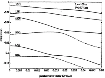
0.57 is used in our calculation. We should note that the usual variational techniques employed are not capable of using different Kohn—Luttinger parameters in the well and the barrier regions.In Fig. 1 we show the valence band structures for (a) F=O KV/cm and (b) F=100 KV/cm of GaAs—Alo.25Gao.75As single quantum well. At K=O, heavy and light holes are exactly decoupled and EU and EL are degenerate, so it is possible to label subbands as "heavy
hole" or "light hole" according to their K=O character. For a nonzero K, the increasing
admixture of light— (heavy—) hole states into heavy— (light—) hole states gives rise to strong nonparabolicities in the valence band structure. Particularly, the light hole (LH1) and heavy hole (HH3) have a negative effective mass at the zone center. This would lead to high joint density of states. In the absence of an external field, the upper and lower block Hamiltonian would give degenerate energy bands for finite I(. However, when an electric field is applied,the breaking of symmetry causes the EU and EL to split for a finite K# This lifting of the
twofold spin degeneracy is due to the lack of symmetry and the presence o(spin—orbit coupling.3.2. Exciton binding energy
The exciton problem are solved by using two different models. One is the
conventional model that assume the same effective mass of heavy—hole (mhh
=
(O.34+O.42x)riio) and light—hole (mlh
=
(O,094+O.043x) mo) at different quantum number states. The othermethod is to calculate the effective mass of each subband state at IC=O. The exciton binding energies versus electric field of GaAs—Alo.25Gao.75As quantum well with 100 A width are
calculated, and the exciton peak energies versus electric field are shown in Fig. 2. With
increasing electric field, the exciton peak positions shown downward shift in the two models. This is the so—called quantum— confined Stark effect. The averaged excitons radius in the zyplane versus electric field are also calculated. We find the dissociation of excitons with
increasing electric field, except HH2 related excitons. This is in coincidance with the binding energy results.The theoretical results in comparsion with the experimental data (after ref 25) is shown in Fig. 3. We find that it shows very good agreement with our results in the order of a few meV in the large field condition. This can be attributed to the tunneling effect. Generally speaking, when the quantum well with an applied electric field perpendicular to the wells, the subband state is no longer a stationally bound state. The carriers will tunnel out of the well region in a longer lifetime, this is the so—called quasi—bound state. From the wavefunctions of
the electrons and holes at the zone center for various electric field, we find that the
increasing the electric field, the resonance time will be decreased in the well, and the 1'effective" well width will be increased. Thus, the subband energies will decrease when the electric field strength increases.
3.3. Optical dipole matrix element
The averaged optical matrix element for transitions between the different
conduction and valence subbands of the QW's for either the TE polarization or the TM
polarization with applied electric field (a) F=O KV/cm, (b) F=50 KV/cm, (c) F=100 Ky/cmcan be calculated. The dependence of optical matrix element on k in the results of the
calculations is due both to mixing of the wave functions, and to the angular dependence of the projections of the transition matrix elements on the different axes (TE or TM polarization). It should be noticed that the optical matrix element are averaged for the angle 0 and upper andlower block.
In bulk semiconductor the optical matrix element is a slowing varying function of k and may safely be approximated by its value at k=O. This This approximation has also been made by a number of authors in the study of superlattices and quantum wells. The widely known Ln = 0selection rule for transitions between subbands is based on the observation that in the envelope—function approximation Mim vanishes unless 1 = m. However, it has been pointed out that for superlattices and quantum wells the approximation Mirn () Mim (0) is a poor one. We find that
Mim(k) 2
is rapidly varying even for small values of k due to the strong mixing of heavy— and light—hole states by the off—diagonal elements in the valence band Halmiltonian Hp,,.For TM polarization by increasing electric field, we find that optical moment matrix element of the E2—HH1 transition increases and that of the E1—HH1 transition decreases. This can be attributed to the wavefunctions of the first and second conduction subbands exhibit opposite behavior (see Fig. 4). For TE polarization, the optical moment matrix elements of the E1—HH2 and E1—HH3 transitions get stronger with increasing electric field is due to the same reason as above description. So, we can expect the absorption spectra will change from the staircase function to multipeak profile for TE polarization with increasing electric field.
3.4. Absorption coefficien
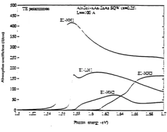
In Fig. 5 we have plotted some of the typical component absorption spectra
aim(hw), for subband—tosubband transitions involving the first four valence subbands and the first two conduction subbands for a 100 A GaAs—Alo.25Gao.75Asquantum well for the TM andTE polarization. The subband—to---subband transitions are quite complicated and the rapidly varying nature of the individual subband absorption reflects the valence band mixing. The total band—to—band absorption spectra for TM polarization are shown in Fig. 6. It is found that the
overall shape of the total absorption spectra obtained by adding up the individual
subband—to--subband absorption curves is close to the staircase function. The peak structure for the E1—LH1 transition is due to the negative zone center effective mass of the LH1 subband. The electronlike curvature of the Lu subband gives the E1—LH1 transition an exceptionally large joint density of states at the band edge, hence the sharp peak near 1.575 eV.
The band—to—band absorption spectra versus electric field are shown in Fig. 7 at 5
OK. With increasing electric field, the spectra are shifted to lower energy side. This is
qualitatively in agreement with the published experimental observations of D. A. B. Miller etal. and Yamanaka et al26. We can find that the absorption spectra change from the
approximately staircase function to the multipeak profile due to the applied electric field. This is the same as that we have expected from the optical moment matrix element results.
226/ SPIE Vol. 1813 Optoelectronic Component Technologies (1992)
3.5. Spontaneous emission rat
Fig. 8 shows the luminescence spectrum (spontaneous emission rate) at 5 OKin the zone field condition. Here we assume the carrier densities are equal to lxlO'7 /cm3. We find that there is a remarkable difference between the TM polarization and TE polarization in both peak energy and amplitude. The experimental data of Sooryakumar et al.2' can be used for qualitative comparison. Because the sample used in the measurement is a modulation—doped 220 A quantum well, so the many—body effect should be included. However, the theoretical
peak position
and peak amplitude are qualitatively in agreement. We also show the
luminescenes spectra at different carrier densities and a different electric field strength at 300OK. Theexpected energy shifts with increasing electric field are also observed for both the TE
and TM polarization. With increasing the carrier densities, we find that the E2—HH2 transition gets stronger relative to the E1—HH1 transition for the TE polarization. This is due to the partial fill of the second conduction band in the high carrier density condition.
3.6. Gain profile and refractive index variation
The calculated results of the gain spectra for a single quantum well structure with well width L=100 A at 300 OK are shown in Fig. 9 for TM polarization for various carriers densities. It is noted that the spectrum of the TE polarization has a peak at E1—HH1 transition energy. For TM polarization, we find that the peak gain occurs at the E1—LH1 transition energy. The resulta are compared with the experimental results of as shown in Fig 9(b). Our
results are in good agreement with the experimental ones in the gain profile, and the gain
amplitude (the threshold carrier density is approximately 2.7x10'8/cm3 and the loss is
approximately 100 /cm). In Fig 10, we show the typical gain spectra versus electric field and temperature. It can be seen that the applied transverse electric field deduces a red shift to the peak gain and reduces the peak gain. The peak gain is reduced by about a factor of 2 when F =100 KV/cm compared to that of the zero—field case. These field—induced gain changes can be applied to tunable lasers and optical switching. The temperature effect on the gain spectrum is due to the band gap shrinkage.
We also calculate the refractive index variation for the single quantum well
structure with a well width 100 A
at 300 OK for TE polarization and TM polarization for various carrier densities. Our results show that the maximum refractive index change is about one percent. From the field—induced refractive index variation for the two polarization modes.We find that the maximum refractive index change is reduced and it varies more smoothly with increasing field strength for the TE mode, and it is not sensitive to the field strength for TM polarization. We also note that the refractive index change in thr active region is negative. Thus, it will result in the defocusing effect, then deduce large optical loss.
4. Conclusion
The effect of valence band mixing and transverse electric field on the absorption coefficient, spontaneous emission rate, gain spectra and refractive index change have been studied by the multiband effective mass theory and the density—matrix method with intraband
relaxation taken into account. We find that the electronic valence band structure is very
complicated due to strong mixing of the heavy and light hole. The valence subband are highly nonparabolic and in particular some valence subbands have negative zone center effective mass. Excitons associated with negative zone center masses tend to have enhanced bindingenergy. The calculated exciton binding energy in our model shows obvious difference in
comparison with the results calculated by conventional model, and the calculated exciton peak energy versus electric field shows good agreement with the experimental results. The absorption coefficient and spontaneous emission rate show distinct Stark shift.The calculated gain in our model shows remarkable difference both in the spectra shape and the peak amplitude as compared to those from the conventional models. The peak
gain is reduced and the gain spectrum is more symmetric and closer to the experimental
observations in our model. The refractive index decrease in the active region, and possibly results in a defocusing effect.5. REFERENCES
1 R. L. Green and K. K. Bajaj, J. Vac. Sci. Technol., B1(2), 391 (1983).
2 G. Bastard, J. Luminesc., 30, 488 (1985).
3 D. A. B. Miller, D. S. Chemla, T. C. Damen, A. C. Gossard, W. Wiegman, T. H. Wood and C. A. Burrus, Phys. Rev., B32, 1043 (1985).
[4] E. E. Mendez, G. Bastard, L. L. Chang, L. Esaki, H. Morko, and It. Fischer, Phys. Rev.,
B26, 7101 (1982).
[5] D. A. B. Miller, D. S. Chemla, T. C. Damen, A. C. Gossard, W. Wiegman, T. H. Wood
and C. A. Burrus, Phys. Rev. Lett., 53, 2173 (1984).
6] D. A. B. Miller, J. S. Weiner and D. S. Chemla, IEEE J. Quantum Electron., QE—22, 1816
1986).
7] D. A. B. Miller, D. S. Chemla, T. C. Damen, A. C. Gossard, W. Wiegman, T. H. Wood and C. A. Burrus, Appi. Phys. Lett., 45, 13 (1984).
[8]
D. Kasemset, C, Hong, N. B. Patel and P. D. Dapkus, IEEE J. Quantum Electron.,
QE—19, 1025 (1983).
9] M. Asada, A. Kameyama and Y. Suematsu, IEEE J. Quantum Electron., QE—20, 745
1984).
101 M. Yamada, S. Ogita, M. Yamagishi and K. TAbata, IEEE J. Quantum Electron.,
QE—21, 640 (1985).
11 Y. Arakawa and A. Yariv, IEEE J. Quantum Electron., QE—21, 1666 (1985). 12 J. N. Schulman and Y. C. Chang, Phys. Rev., B31, 2056 (1985).
13 G. D. Sanders and Y. C. Chang, Phys. Rev., B35, 1300 (1987).
14 S. Colak, R. Eppenga and M. F. H. Schuurmans, IEEE J. Quantum Electron., QE—23, 960
1987).
15 S. C. Hong, M. Jaffe and J. Singh, IEEE J. Quantum Electron., QE—23, 2181 (1987). 16 D. Ahn and S. L. Chang, J. Appi. Phys., 64, 4056 (1988
17 J. M. Luttinger and W. Kohn, Phys. Rev.,97, 869 (1955. 18 G. D. Sanders and Y. C. Chang, Phys. Rev.,B32, 5517 (1985). 19 J. A. Brum and G. Bastard, Phys. Rev., B31, 3893 (1985).
20 D. Aim and S. L. Chang, IEEE J. Quantum Electron., QE—23, 2196 (1987).
21 L. Vina, R. T. Collins, E. E. Mendez and W. I. Wang, Phys. Rev. Lett., 58, 832 (1987). 22 N. Bloembegren, Nolinear Optics. New York: Benjamin, 1965, Ch. 2.
23 G. Lasher and f. Sterm, Phys. Rev., 133, A553 (1964).
24 P. Blood, E. D. Fletcher, P. J. Hulyer and P. M. Snowton, Appi. Phys. Lett., 48, 1111
1986).
25] Y. Kajikawa, Nao—haru Sugiyama, T. Kamijoh and Y. Katayama, J. J. Appi. Phys., 28,
L1022 (1989).
26] K. Yamanaka, T. Fukunage, N. Tsukada, L. I. K. and M. Ishii, Appl. Phys. Lett., 48, 840
1986).
27] R. Sooryakumar, D. S. Chemla, A. Pinczuk, A. C. Grossard, W. Wiegmann and L. J. ham, Solid State Commun., 54, 859 (1985).
228/ SPIE Vol. 1813 Optoelectronic Component Technologies (1992)
Taale L Ixznabandrelaxañon thne as a fuxndon of zernperazure e lisred:
[IT (K)I
T(P5)130010.1
0.14 5 0.2Table II. Band paramere of GaAs and AAs
F__ GaASA1AS
0.067
r1 6.85 j 3.45
r
[ r3
io
1.29Table IlL Band parainete of in? and 1nGaAs
In? IX3Ga0c.As I 0.041 r1 13.95 3.45 5.69 0.68 r3 6.07 1.29 Eg (cV) 0.812 1.425
Fig.1.(a) Valence band sntnire fora 100AA0Ga0A.vC3As
single quannim well withno applied elecinc geld F= KV/cn..
u.
L=lOOA am- m: ?=100 }VkxnmL;
.L
. O7 -0 0.005 0.01 0.015 0.02 0.025 0.03 0.035 0.04 0.045 0.05xaflcIwave ve 1CU(1L)
FigL) Valence band smzcmre fora 100A .k35\Ja0.75As/GaAs
singlenuann well with applled e1eicñei. F00KV/cn.
L5r
31 fid sncgm (KV;=nl
Fig- 2. ' Averageet0fl peal: e::er;ies at 300 O(
suobanda first fc- valance subbanos as a funce.n of eiic ñeid
ina 100A A105G.t75As/GaAs single quannian welL
F:43 Crnpndson eween cnl=.ited (scud line) and
z-anadRef:9) (sr) vaes of the hea.hole ex&.cn ed lig±u-ie
exalzone=gies esafunceon oieien-c f.nidseT K ia 0
A (100) odaneed .JnGaAseGaAs cuannm well
snzre-lef wave we KU(1/A)
.. LwziOO A T=300 K . El-MIll 1.51 1.49-& ll=c 1d sng (KVIn,
230 1 SPIE Vol. 1 8 1 3 OptoelectroniC Component Technologies (1992)
• '50- . tx Ai-xAs.aAs -. - SQ tX — 400-
\
- :50- zoo- - 50- 0 .Fig 4' Average squared zpoie m .errx eent
onducion subband and Ers four vainc suands as a fre.n
eIecthc eid in a 100 A A
Gao.-5ASiGaAS single uan weil
with aopiied electric eid F=00 KVin for TM poiznon
Fig.
5
Sub-o-subbaosonon coefñcienz for nszons
frain .e four nce sx—bands :o the first condurñon suIand
at 5 'K in 100 A
.
AsCAs single
quaurn eil with
TE mnon.
Fig.6
single quar.n well with T
olarlzazion.
Fig.
)
nsecaversuseiecin:ñeld5 :Ka 100A A3.A3GOAS 3Z1C QttWO WC. with T!
,olaz-.=ion.
,
K/(LA) I TE po '000 s00 6c0 I°-• < 200— ;I-LAs,ca:As SQ T= K !:-:.-:: _i_5 1.6 :.eSP•.=on eiin•5• IeV)
- 1-s 4500- O_'!' L.=i00A T=5
)
stv/= 4000— -. . ——-—-.:: • . 35co 30C0— ••••...-• sco- . 2000- .//
1500- 1000- - 500— .•.
x10 10 i.=00A - 8;- 1
"
. —/
VY22J
I
A
6- 5.I
4./
\
- S/
- :V)Fig. Poiaron ece of the
sponneous ssion sea
at
5
'K in a 100 A Al3e,-ALGa sineie qu welL
Fig.
)
Gain szea for fou differez amr densines ax 300 'KInc 00 AAlG5AS1GaAS
single qncnaxl well for foor different
dsines with TM polarlon-
Fig. ?t'b) The expenmxl gatn peca of -L i:ayasth a: aL
are incL.e for ::iparson (wthere the Al .nCSiO1 S
232
I
SPIE Vol. 1813 Optoelectronic Component Technologies (1992)Pbn ery (aV) 0 too' 1 s- -:=re
-
-
-
z -n)- -co- i.Wc
]
1
-o- 000-
8500 EWO .wcvee'th.AI
Gain sp:.a br wid TM pr'iarsaz:w!owr -i.2-v :.—.. :..-5 :.8 L :... L5 1.62 (:V) .10 c21 wc th -=-=.< :r:St.2