© 2017 IJSRST | Volume 3 | Issue 1 | Print ISSN: 2395-6011 | Online ISSN: 2395-602X Themed Section: Science and Technology
Influence of Annealing Temperature on Optical and Electrical Properties
of Cu
2ZnSnS
4(CZTS) thin Films Deposited by Sputtering Method from a
Single Quaternary Target
S. Abdullahi*1, M. Momoh1, A.U. Moreh1, A. M. Bayawa2, B. Hamza1, G.M. Argungu1, O. T. Popoola3
1Department of Physics Usmanu Danfodiyo University Sokoto, Nigeria
2Department of Pure and Applied Chemistry Usmanu Danfodiyo University Sokoto, Nigeria
3Department of Mechanical Engineering Florida International University Miami, Florida, U.S.A
ABSTRACT
Cu2ZnSnS4 thin films were fabricated by one-step RF magnetron sputtering of a single quaternary Cu2ZnSnS4 (CZTS) chalcogenide target on corning glass substrate, followed by annealing at 523, 623 and 723K under nitrogen atmosphere for 60 minutes. Optical transmittance and reflectance data of the films were utilized to compute the absorption coefficient, refractive index, extinction coefficient and optical band gap energy of the films. The nature of the optical transition has been direct allowed with average optical band gap energies ranging between 1.5 eV and 2.4 eV. The optical band gap energy has a tendency to increase with the increase in the annealing temperature. The resistance and sheet resistance of the films ranges from 4.1 -3Ω cm-14680
-3Ω cm and 0.02
3Ω-0.25
3Ω respectively.
Keywords: RF sputtering, Cu2ZnSnS4 Thin Film, Annealing, Resistance, Optoelectronics.
I.
INTRODUCTION
Cu2ZnSnS4 (CZTS) quaternary compound exhibits optimum parameters for solar cell materials, namely absorption coefficient of over 104
cm-1 and band-gap energy of 1.5 eV [1-2]. It is earth abundant, non-toxic and environmental friendly [3]. This material (CZTS) has attracted considerable interest due to its potential in solar cell application and optoelectronics.
Its crystalline structure is commonly referred to as Kesterite. This structure is strongly related to the Chalcopyrite structure of a well-known photovoltaic absorber material Cu (In, Ga)Se2 with the record efficiency of 20.3 % [4]. A pure CZTS absorption layer with a dense microstructure is the key factor to prepare high efficiency solar cells.
CZTS thin films have been prepared by vacuum and non-vacuum methods, such as sol-gel [5], RF magnetron sputtering [6-9], co-sputtering [10], Hot injection method [11], thermal evaporation [12] and electron beam evaporation [13]. Among these methods, RF sputtering is the simplest because all the deposition
parameters more importantly the film thickness can be controlled. It can be applied to large area and still maintaining uniform distribution of the deposited material on the substrate. Sputtering CZTS from a quaternary single target on the other hand is a quick and reproducible process, in agreement with the industry needs.
In this work, the influence of annealing temperature on
the optical and electrical properties by UV
spectrophotometer and four-point probe is investigated as reports of CZTS thin films below 1000nm thick are scarce. The samples were of 450nm thickness. After the deposition, the samples were annealed at 523, 623 and 723K respectively. In all, four samples were deposited one of which is the as-deposited or reference sample.
II.
METHODS AND MATERIAL
A. Materials
The quaternary target (obtained from AJA international)
is 99.99% pure. The elemental ratios were
Detergent, distilled water, ethanol and isopropanol were used for substrate cleaning. Argon of 99.99% purity has been used as the carrier gas while the annealing was done under nitrogen atmosphere.
B. Material synthesis and method
Prior to the deposition, the substrates were cleaned by the normal substrate cleaning procedure. CZTS thin films of 450 nm thickness were deposited on corning glass by RF sputtering form a single quaternary target. The sputter vacuum chamber was exiled to less than 4.6 Pa. Ar gas flow rate was maintained at 20 sccm. The operating pressure during CZTS sputtering was maintained at 5.6 Pa, the RF power used was 75 W. Substrate temperature remained throughout the deposition at 373K.
C. Annealing of the samples
Three samples of average thickness 450nm were annealed at 523, 623 and 623K under flowing nitrogen. The ramp rate was 283K per minute and the dwelling time was 1 hour. The purity of the nitrogen gas is 99.99%. The fourth sample has been kept as the as-deposited.
D. Characterization tools
Transmittance, reflectance and absorbance data obtained
from spectrophotometer (AVANTES AVASPEC-2048
UV-VIS-NIR) was used to determine optical properties such as absorption coefficient extinction coefficient, refractive index and the energy band gap. The spectrophotometer was operated in the wavelength length of 180-1100nm. The electrical properties of the samples were measured by four-point probe (Keithley model 181 nanovolt electrometer). All the characterizations were done at room temperature.
III.
RESULTS AND DISCUSSION
A. Optical characterization
Figure 1 represents the optical spectra of the as-deposited sample of 450 nm thickness. The sample is having an average transmittance of 0.0092%. This is a clear indication that the sample is almost opaque. This
indicates that this films grow with a high density of native defects (vacancies, interstitial and antisite). [14] suggested that these defects generate absorption centres within the energy gap which contribute to the photon absorption.
Figure 1: Transmittance versus wavelength for as deposited sample.
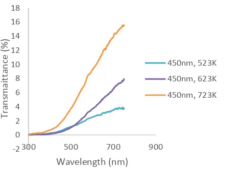
Figure 2 shows the transmittance of the samples annealed at 523, 623 and 723K. The average transmittance for each sample is 4%, 8% and 16% respectively. As the annealing temperature increases, the transmittance increases. Low transmittance values in thin films indicates high absorption [15]. The surface roughness of the films affected the film transmittance by both reflecting the incoming light and reducing the
transmittance. This explains the difference in
transmittance of the CZTS films [7,16]. The absorption edge for the films annealed at 623 and 723 is around 450nm which is suitable for solar cell absorber.
Figure 2: Transmittance versus wavelength for samples annealed at 523, 623 and 723K.
When a particular type of radiation is incident on a surface, the radiation is either transmitted, reflected or absorbed by the material of the surface. Figure 3 shows the reflectance spectra of the as-deposited sample and
-2 0 2 4 6 8 10 12 14 16 18
300 500 700 900
Tra
n
sm
ait
ta
n
ce
(%
)
Wavelength (nm)
450nm, 523K 450nm, 623K
the samples annealed at 523, 623 and 723K respectively. The fact that the samples shows high reflectance is an indication that there is high scattering of light on the samples. From Figure 3 it can be seen that the as-deposited sample is having the lowest reflectance (45%) while the sample annealed at 723K possesses the highest reflectance (80%). Another possible reason for the high reflectance may be the presence of the coherence between the primary light beam and the beam reflected between the film boundaries is lost and results in the disappearance of interference which in turn decreases the transmittance. Increase in annealing temperature results in the increase in the reflectance.
Figure 3: Reflectance spectra versus wavelength of the as-deposited sample and samples annealed at 523,623
and 723K.
The optical band gap of all the CZTS thin films was obtained using equation (1) [1,14,17];
( ) ( ) (1)
Where, is the optical absorption coefficient, A is a constant, Eg is the optical band gap and n = 1/2 for direct transition. The optical band gap was obtained by extrapolating the linear region of the plot ( )2
versus
. Absorption coefficient ( ) was determined from the measured transmittance (T) and reflectance (R) using relation (2) [9, 16,18],
( ) (2)
where, is the absorption coefficient, d is the film thickness, R, reflectance and T, the transmittance respectively.
For a semiconductor, the light penetration depth, d, is
roughly given by d = where is the absorption
coefficient [19]. The extinction or attenuation coefficient (K) is directly proportional to the absorption coefficient (α) according to relation (3) [17],
(3) where λ is the wavelength of light.
The refractive index (n) is a mathematical coefficient, which tells about the passage of light through the material. The index is calculated from equation (4) [20];
(
) ( )
⁄ (4)
Optical band gap (Eg) of the samples was deduced from the plot of ( ) versus , by extrapolating the straight line portion of the graph in the high absorption regime, where are absorption coefficient and incident photon energy. The ( ) versus plots for as-deposited and films annealed at temperatures of 523, 623 and 723K is shown in Figure 4. The direct optical band gaps are found to be 1.80, 1.52, 2.00 and 2.30 eV, respectively. From this, the band gap energy (Eg) of the film deposited at 523K is quite close to the optimum value for CZTS. It has been observed that the as-deposited and the films as-deposited at 623K and 723K exhibited much higher band gap than the film annealed at 523K. The presence of ZnS phase causes the enlargement of the optical band gap since this phase has a large band gap of 3.5eV. It has been noted that the value of the band gap for the annealed samples though influenced by secondary phases increases with increase in the annealing temperature.
Figure 4: Photon energy (eV) versus (ahv)2 for of as- deposited sample and samples annealed at 523, 623 and
723K.
10 20 30 40 50 60 70 80 90
350 550 750 950
Re
fle
ctan
ce
(%
)
Wavelength (nm
450nm, as-deposited 450nm, 523K 450nm, 623K 450nm, 723K
0 5 10 15 20
0 0.5 1 1.5 2 2.5 3 3.5 4
(
𝑎
𝑣
)2
(e
V cm
-1)2
Photon energy (eV)
as-deposited, 450nm 523K, 450nm
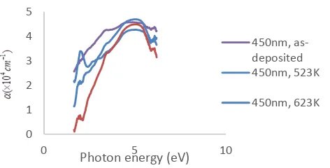
The value of the absorption coefficient of the samples is observed to fluctuate with respect to film thickness. Figure 5 shows the absorption coefficient α (cm-1
) versus photon energy (hv) for as-deposited CZTS thin films and the samples annealed at 523, 623 and 723K respectively. All the samples showed absorption coefficient greater than 104 cm-1 and fundamental absorption edges with complex structures. According to the Hopfield quasi-cubic model for copper-containing compounds, this complex near-edge spectrum is determined by the p–d hybridization of the compound’s valence band [1].
Figure 5: Photon energy versus absorption coefficient of as-deposited sample and samples annealed at 523,
623 and 723K
Table 1 presents the calculated values of extinction coefficient and refractive index. The change in the K shows that a fraction of light was lost because of scattering. The change observed in the refractive index indicates normal dispersion behaviour. It can also be due to thermal induced growth of grains, which increases the packing density according to [17].
TABLE 1
SOME OPTICAL CONSTANTS CALCULATED FROM TRANSMITTANCE/REFLECTANCE DATA
S/no Thickness, annealing temperature
Extinction coefficient
Refractive index
1 450nm,
as-deposited
1.2 1.41
2 450nm, 523K 1.29 1.37
3 450nm, 623K 9.93 1.33
4 450nm, 723K 4.60 5.34
B. Electrical characterization
The grown films were subjected to electrical characterization by use of a 4-point probe. A probe head with tungsten carbide tips with a point radius of 0.002", a probe spacing of 0.05" and a probe spring pressure of 70 to 180 grams was used for all measurements. Current was supplied by a Crytronics model 120 current source with a range of applied currents between 1μA to 100 mA. Voltages were measured by a Keithley model 181 nanovolt electrometer with an input impedance of greater than 1 giga-ohm. Sheet resistance (Rs in units of Ω/sq.) and resistivity (ρ in units of Ω·cm) were determined by equation (5) (Moreh et al., 2014);
(5)
where S is the space between the probes.
Table 2 presents the resistivity and sheet resistance of the as-deposited and films annealed at 523, 623 and 723K. The accuracy of the probe is up to 0.5%. It is clear from the table that the as-deposited sample is having the lowest resistivity while the sample annealed at 723K is having the highest resistivity. The high value of resistivity for the as-deposited samples may be due to the presence of disorder, high density of state and structural defects in the film. According to [22], the change in the resistivity may be due to the metal ratio in the film. It was commonly observed that the Cu and Zn antisites defect is the main cause for the p-type conductivity of CZTS films, for which CZTS films must be Cu-poor and Zn-rich to successfully fabricate CZTS solar cells [23]. The high resistivity observed in the samples may also be due to the existence of shallow states in band gap region resulting in formation of both acceptors and donors leading to self-compensation.
TABLE 2
MEASURED VALUES OF RESISTIVITY ( ) AND
SHEET RESISTANCE (RS) OF CZTS THIN FILMS
S/no Annealin g Temp. (K)
Resistivity (Ω cm)
Sheet resistance (Ω/□)
1
as-deposited
4.1 -3Ω cm
0.02 3Ω/□
2 523K 7.4 -3Ω cm
0.02 3Ω/□ 0
1 2 3 4 5
0 Photon energy (eV) 5 10
450nm, as-deposited 450nm, 523K
3 623K 2280 -3Ω cm
0.20 3Ω/□
4 723K 14680 -3Ω
cm
0.25 3Ω/□
IV.CONCLUSION
In this work, the optical constants considered showed that CZTS possess good optical properties applicable in optoelectronics. The relationship between optical properties and the film thickness/annealing temperature cannot be clearly established because of the dominance of secondary phases in the samples. The appearance of secondary phases is normal in the deposition of CZTS. It has been shown that the absorption coefficient of all the samples is within the required range for the absorption of photons. The transmittance and reflectance increases with increasing annealing temperature
V.
REFERENCES
[1]. I. V. Bodnar, Telesh, E. V., Gurieva, G. and, & Schou, J., "Transmittance Spectra of Cu2ZnSnS4 Thin Films". Journal of Electronic Materials, vol. 4, pp. 2–6(2015).
[2]. J. He, Sun, L., Zhang, K., Wang, W., Jiang, J., Chen, Y., … Chu, J., "Effect of post-sulfurization on the composition, structure and optical properties of Cu2ZnSnS4 thin films deposited by sputtering from a single quaternary target". Applied Surface Science, vol. 264, pp. 133– 138(2013).
[3]. J.C. González, Fernandes, P. A., Ribeiro, G. M., Abelenda, A., Viana, E. R., Salomé, P. M. P., & Da Cunha, A. F., "Influence of the sulphurization time on the morphological, chemical, structural
and electrical properties of Cu2ZnSnS4
polycrystalline thin films". Solar Energy Materials and Solar Cells, vol. 123, pp. 58–64(2014).
[4]. P. Bras, Sterner, J., & Platzer-Björkman, C., "Influence of hydrogen sulfide annealing on copper–zinc–tin–sulfide solar cells sputtered from a quaternary compound target". Thin Solid Films, vol. 582, pp. 233–238(2015).
[5]. A.K.M. Tanaka, K., Nakano, Y., & Uchiki, H.,
"Chemical composition Dependence of
morphological and optical Properties of
Cu2ZnSnS4 thin films deposited by Sol–Gel
Sulfurization Method and Cu2ZnSnS4 thin film solar cell efficiency", 95, 838–842(2011).
[6]. M. Abusnina, Moutinho, H., Al-Jassim, M.,
Dehart, C., & Matin, M., "Fabrication and characterization of CZTS thin films prepared by the sulfurization of RF-sputtered stacked metal precursors". Journal of Electronic Materials, vol. 43, pp. 3145–3154(2014).
[7]. M.I. Amal & Kim, K. H., "Crystallization of kesterite Cu2ZnSnS4 prepared by the sulfurization of sputtered Cu – Zn – Sn precursors". Thin Solid Films, vol. 534, pp. 144–148(2013).
[8]. J. Kim, Park, C., Pawar, S. M., Inamdar, A. I., Jo, Y., Han, J., … Im, H., "Optimization of sputtered ZnS buffer for Cu2ZnSnS4 thin film solar cells". Thin Solid Films, vol. 566, pp. 88–92(2014). [9]. J. Feng, Huang, X., Chen, W., Wu, J., Lin, H.,
Cheng, Q., … Zhang, F., "Fabrication and characterization of Cu2ZnSnS4 thin films for photovoltaic application by low-cost single target sputtering process". Vacuum, vol. 126, pp. 84– 90(2016).
[10]. J. Ge, Wu, Y., Zhang, C., Zuo, S., Jiang, J., Ma, J., … Chu, J. "Comparative study of the influence of two distinct sulfurization ramping rates on the properties of Cu2ZnSnS4 thin films". Applied Surface Science, vol. 258, pp. 7250–7254(2012). [11]. R. Ahmad, Distaso, M., Azimi, H., Brabec, C. J.,
& Peukert, W., "Facile synthesis and post-processing of eco-friendly, highly conductive copper zinc tin sulphide nanoparticles". Journal of Nanoparticle Research, vol. 15, pp.1–16(2013). [12]. M.F.A.I. Alias, Naji, I. S; Mansoor, M.,
"Dependance of structural and morphological
properties on Se concentration for thin
Cu2ZnSnS(SexS1-x)4 FILMS". International
Journal of Advanced Scientific and Technical Research, vol. 2, pp. 26–35(2014).
[13]. H. Araki, Kubo, Y., Jimbo, K., Maw, W. S., Katagiri, H., Yamazaki, M., … Takeuchi, A., "Preparation of Cu2ZnSnS4 thin films by sulfurization of stacked metallic layers". Thin Solid Films, vol. 517, pp. 1457–1460(2008). [14]. G. Gordillo, Calderón, C., & Bartolo-pérez, P.,
pp. 506–514(2014).
[15]. H. ElAnzeery, El Daif, O., Buffière, M., Oueslati, S., Ben Messaoud, K., Agten, D., … Poortmans, J., "Refractive index extraction and thickness optimization of Cu2ZnSnSe4 thin film solar cells". Physica Status Solidi (a), vol. 212, pp. 1984– 1990(2015).
[16]. R. Touati, Rabeh, M. Ben, & Kanzari, M. "ScienceDirect E-MRS Spring Meeting 2013 Symposium D -Advanced Inorganic Materials and Structures for Structural and Optical Properties of the New Absorber Cu2ZnSnS4 Thin Films Grown by Vacuum Evaporation Method"., Energy Procedia, vol. 44, pp. 44–51(2014).
[17]. Maheshwari, Uma and Senthil
Kumar.,"Experimental investigation of an adsorptive thermal energy storage"., International Journal of Energy Research, 39, 771–777(2015). [18]. J. Wang, Li, S., Cai, J., Shen, B., Ren, Y., & Qin,
G., "Cu2ZnSnS4 thin films : Facile and cost-effective preparation by RF-magnetron sputtering and texture control". Journal of alloys and compounds, vol. 552, pp. 418–422(2013).
[19]. P.A. Fernandes, Salomé, P. M. P., & Da Cunha, A. F.,"Study of polycrystalline Cu2ZnSnS4 films by Raman scattering". Journal of Alloys and Compounds, vol. 509, pp. 7600–7606(20110. [20]. M. Yıldırım, Özel, F., Tuğluoğlu, N., Yüksel, Ö.
F., & Kuş, M., "Optical characterization of Cu2ZnSnSe4-xSx nanocrystals thin film". Journal of Alloys and Compounds, vol. 666, pp. 144– 152(2016).
[21]. A.U. Moreh, M. Momoh, B. Hamza, S. Abdullahi,
H.N. Yahya, S. Namadi and S. Umar., "Influence of substrate temperature on electrical resistivity and surface morphology of CuAlS2 thin films prepared by thermal evaporation method". International journal of Nano and Material sciences, vol. 3(1), pp. 47- 55(2014).
[22]. M.A. Islam, Aziz, A., Witjaksono, G., & N. Amin.
(2013). Structural, Electrical and Optical
Properties of Zn Rich CZTS Thin Film, (December), 16–17.