183
Fabrication of Copper and Iron Nano/Micro Structures
on Semiconducting Substrate and Their Electrical
Characterization
J. Kaur
1*, S. Singh
1, R. Kumar
2, D. Kanjilal
3, Sh. Chakarvarti
41- Department of Physics, Guru Nanak Dev University, Amritsar, India
2- Department of Physics, Haryana College of Technology and Management, Kaithal, India
3- IUAC New Delhi, India
4- Manav Rachna International University(MRIU),Faridabad, India
(Received:10 Sep. 2011 and Accepted: 25 Nov. 2011)
Abstract:
In this paper, we have studied the electrical properties of the randomly distributed metallic (Co and Fe) nano/ micro wires on Silicon substrate. Deposition was carried out potentiostatically into the pores of the track-etch
polycarbonate membrane spin coated onto the Si substrate. Spin coated films were irradiated with 150MeV
Ni (+11) ions at a fluence of 8E7 ions/cm2, followed by UV irradiation and chemically etching in aqueous
NaOH (6N, at room temperature). The size, shape and morphology of the synthesized nano/micro structures is strongly dependent on the preparation conditions such as deposition potential, current density, electrolyte and etching conditions. Later, morphological and electrical properties of the so deposited nano-/micro structures were studied.
Keywords: Irradiation, Ion track, etching.
Int. J. Nanosci. Nanotechnol., Vol. 7, No. 4, Dec. 2011, pp. 183-189
1. INTRODUCTION
In the recent years, there has been tremendous in-terest exhibited towards nano and micro pores in polymers generated by swift heavy ions due to vast
variety of applications [1,2]. The technological im
-portance of track-etched membranes is very signifi -cant due to their various applications particularly
in the field of nano-/micro structural synthesis and
their further use as devices in electronics. The pores are created by controlled chemical etching of the latent track created by irradiation of the polymeric
film. The highly selective etching of tracks in poly -carbonate makes it possible to produce membranes
with pore diameters down to 10 nm [3]. By vary
-ing the ion fluence and the etch-ing conditions, pores
of different sizes and geometries are possible. This template technique enables the fabrication of wires with various shapes, in particular, conical or cylin-drical.
The research on nano-/micro structures has led to
the exploration of novel physics and material prop-erties at reduced physical dimensions. There is con-siderable technological interest in the fabrication of arrays of high aspect ratio structures synthesized by electrodeposition for use as sensors and ultra-high-density information storage. Along with the
synthesis of bare nano/micro structures, fabrication
of one-dimensional nanostructures, or nanowires on the substrate (metallic or semiconducting), has been under intense investigation due to their lucrative
184
11 Table 1:-
Slope Intercept
Copper 2.22 6.26E-7
Iron 1.24 2.88E-6
Polymeric film
Au
Si substrate
Fig 1. Systematic picture of the template used for deposition.
Figure 1: Systematic picture of the template used
for deposition.
In the present work, the track-etched membrane is
used to synthesis nano-/micro structures on the sub -strate itself. Structures are grown directly over the semiconducting substrate for their further charac-terization and obviating the need for post- synthesis
manipulations. These Semiconductor based nano-/
micro structures are expected to have practical
ap-plications in electronic circuit integration [7,8]. A
thin polymeric layer was spin coated on the gold-coated semiconducting substrate. This gold layer acts as electrode at the time of electrodeposition and polymeric layer acts as template having the etched tracks.
2. EXPERIMENTAL DETAILS
Preparation of substrate was carried out at Inter University Accelerator Center (IUAC), New Delhi, India, and the CSIO, Chandigarh, India. We have used Si (P-doped) (111) as a semiconducting substrate. To remove the dirt and oxide layer from the surface of the substrate Si, wafer was kept in Trichloroethylene solvent at 70 oC for 10 min then
immersed in 1% HF acid for 1 min. Finally wafer was rinsed using deionised water for 5 min.
A thin gold layer with thickness of about 95.5 nm
was deposited using vacuum evaporation method, onto the Au layer, polycarbonate (Makrofol) was deposited by spin coating (at room temperature with spinning speed of 4000 rpm) and the thickness of
coated polymer was around 10 μm. The adhesion of the polycarbonate film on the substrate was improved
by the use of a primer (hexamethyledisilisazan), a
chemical reagent (CH3)3Si-NH-Si(CH3)3, consisting of ammonia substituted with two trimethylsilyl functional groups.
12
Figure 2(a) SEM image of the etched pores on PC coated semiconducting substrate
irradiated with Ni (150) MeV ions
Figure 2(b) SEM image of the electrodeposited copper nano/micro wires on the Si
substrate.
Figure 2(a): SEM image of the etched pores on PC
coated semiconducting substrate irradiated with Ni (150) MeV ions
12
Figure 2(a) SEM image of the etched pores on PC coated semiconducting substrate irradiated with Ni (150) MeV ions
Figure 2(b) SEM image of the electrodeposited copper nano/micro wires on the Si
substrate.
Figure 2(b): SEM image of the electrodeposited
copper nano/micro wires on the Si substrate.
13
Figure 2(c) SEM image of the electrodeposited iron nano/micro wires on the Si substrate
-2 -1 0 1 2
-1.0x10⁻⁵
0.0 1.0x10⁻⁵
2.0x10⁻⁵
3.0x10⁻⁵
4.0x10⁻⁵
0.0 0.5 1.0 1.5 2.0 5.6028E-9
1.523E-8 4.13994E-8 1.12535E-7 3.05902E-7 8.31529E-7 2.26033E-6 6.14421E-6 1.67017E-5
ln
(I)
Voltage
Curr
ent
Voltage
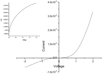
Figure 3 (a) I-V characteristics of embedded copper nano/micro wires on Si substrate. Inset shows the variation of ln(I) with voltage(V).
Figure 2(c): SEM image of the electrodeposited
iron nano/micro wires on the Si substrate
185
13
Figure 2(c) SEM image of the electrodeposited iron nano/micro
wires on the Si substrate
-2 -1 0 1 2
-1.0x10⁻⁵
0.0 1.0x10⁻⁵
2.0x10⁻⁵
3.0x10⁻⁵
4.0x10⁻⁵
0.0 0.5 1.0 1.5 2.0 5.6028E-9
1.523E-8 4.13994E-8 1.12535E-7 3.05902E-7 8.31529E-7 2.26033E-6 6.14421E-6 1.67017E-5
ln
(I)
Voltage
Curr
ent
Voltage
Figure 3 (a) I-V characteristics of embedded copper nano/mic
ro wires on Si substrate.
Inset shows the variation of ln(I) with voltage(V).
-4 -2 0 2 4 6
-4.0x10⁻⁴ -2.0x10⁻⁴ 0.0 2.0x10⁻⁴ 4.0x10⁻⁴ 6.0x10⁻⁴
0 1 2 3 4 5
8.31529E-7 2.26033E-6 6.14421E-6 1.67017E-5 4.53999E-5 1.2341E-4 3.35463E-4
ln
(I
)
Voltage
cu
rrent
Voltage
Figure 3(b) I-V characteristics of embedded iron nano/micro wi
res on Si substrate. Inset
shows the variation of ln(I) with voltage(V).
0.0 0.5 1.0 1.5 2.0
0.0 0.5 1.0 1.5 2.0 2.5
Co
nt
ac
t Res
is
tan
ce
(
X
10
-6 )
Voltage(V)
Figure 3(b): I-V characteristics of embedded iron nano/micro wires on Si substrate. Inset shows the
variation of ln(I) with voltage(V).
Figure 3 (a): I-V characteristics of embedded copper nano/micro wires on Si substrate. Inset shows the
variation of ln(I) with voltage(V).
186
The prepared samples were irradiated at room
temperature with 150 MeV Ni+11 ions at a fluence
of 8E7 at IUAC, New Delhi, India. Later, the irradiated samples were UV treated (365 nm, 150 W/cm2) to increase the selectivity of the
chemical etching thus favoring the formation
of cylindrically shaped pores. Etching was
performed in a home made one-compartment cell with a 6N NaOH aqueous solution at room
temperature for a time up to 50 min.
14
-4 -2 0 2 4 6
-4.0x10⁻⁴ -2.0x10⁻⁴ 0.0 2.0x10⁻⁴ 4.0x10⁻⁴ 6.0x10⁻⁴
0 1 2 3 4 5 8.31529E-7 2.26033E-6 6.14421E-6 1.67017E-5 4.53999E-5 1.2341E-4 3.35463E-4 ln (I ) Voltage cu rrent Voltage
Figure 3(b) I-V characteristics of embedded iron nano/micro wires on Si substrate. Inset
shows the variation of ln(I) with voltage(V).
0.0 0.5 1.0 1.5 2.0
0.0 0.5 1.0 1.5 2.0 2.5 Co nt ac t Res is tan ce ( X 10 -6) Voltage(V)
Figure 4: The variation of resistance with applied
bias for the Copper nano/ microwires on Silicon substrate
15
Fig 5(a). The variation of resistance with applied bias for the Copper nano/ microwires on
Silicon substrate
0 1 2 3 4 5
0.00 0.02 0.04 0.06 0.08 0.10 0.12 cont ac t r esist ance (X 10 -6 ) Voltage (V)
Fig 5(b). The variation of resistance with applied bias for the Iron nano/ microwires on
Silicon substrate
30 32 34 36 38 40
0 10 20 30 40 50 60 current ( m icroam p) voltage
Figure 5: The variation of resistance with applied
bias for the Iron nano/ microwires on Silicon substrate
The supported films were then immersed in an ace -tic acid solution and rinsed with milli-Q water at
room temperature for 5 min and were then dried
with hot air. It must be noted that the pore size de-pends both on the conditions of the ionic and UV irradiation, and on the conditions during chemical treatment of the tracks like nature and concentration of the reactants, temperature during etching, time duration for etching.
UV exposure leads to photo-oxidation in the poly-carbonate and is able to increase the track etch ratio
by an order of magnitude [9].
15
Fig 5(a). The variation of resistance with applied bias for the Copper nano/ microwires on
Silicon substrate
0 1 2 3 4 5
0.00 0.02 0.04 0.06 0.08 0.10 0.12 cont ac t r esist ance (X 10 -6) Voltage (V)
Fig 5(b). The variation of resistance with applied bias for the Iron nano/ microwires on
Silicon substrate
30 32 34 36 38 40
0 10 20 30 40 50 60 current ( m icroam p) voltage
Figure 6 (a): I-V curve of copper nano/micro wire
on semiconducting substrate
17
2.5 2.6 2.7 2.8 2.9 3.0 3.1
-1 0 1 2 3 4 5 6 ln (I/E 2 ) 1/E
Fig 7 (b) F-N plot of iron nano/micro wire on semiconducting substrate
Figure 6 (b): F-N plot of copper nano/micro wire
on semiconducting substrate
187
Electro-deposition within these pores of thesupported template was performed at room temperature in a conventional one-compartment cell, with a copper rod working as anode and the gold layer as working electrode (cathode). An aqueous solution of FeSO4 + H2SO4 and CuSO4 + H2SO4 respectively, was used as electrolyte for the deposition of iron and copper into the pores.
16
Fig 6 (a) I-V curve of copper nano/mi
cro wire on semiconducting substrate
2.5 2.6 2.7 2.8 2.9 3.0 3.1
1 2 3 4 5 6 7
ln(I
/E
2 )
1/E
Fig 6 (b) F-N plot of copper nano/mi
cro wire on semiconducting substrate
30 32 34 36 38 40
0 10 20 30 40 50
cu
rre
nt
(micr
oamp)
voltage
Fig 7 (a) I-V curve of iron nano/mi
cro wire on semiconducting substrate
Figure 7 (a): I-V curve of iron nano/micro wire on
semiconducting substrate
16
Fig 6 (a) I-V curve of copper nano/micro wire on semiconducting substrate
2.5 2.6 2.7 2.8 2.9 3.0 3.1
1 2 3 4 5 6 7
ln(I
/E
2 )
1/E
Fig 6 (b) F-N plot of copper nano/micro wire on semiconducting substrate
30 32 34 36 38 40
0 10 20 30 40 50
cu
rre
nt
(micr
oamp)
voltage
Fig 7 (a) I-V curve of iron nano/micro wire on semiconducting substrate
Figure 7 (b): F-N plot of iron nano/micro wire on
semiconducting substrate
High concentration of electrolyteis important to
provide a sufficiently large number of ions inside the pores during the galvanic deposition process. Nano-/
micro structures were grown potentiostatically at 0.4 V. The deposition potential was applied using a power
supply (Electromek INDIA, SAM- Model MR 85, 15
V) and the current and potential drop across the cell was monitored by digital multimeter (PHILIPS Digital
Multimeter 1225).
After the deposition, substrate with nano-/micro wires
was immediately removed from the electrolyte and then rinsed with double-distilled water and ethanol. Finally, it was dried in dry air at room temperature and subjected to further analysis. The porous thin polycarbonate membrane was removed by dissolving it in dichloromethane for 10 minutes and washed several times with double-distilled water.
3. RESULTS AND DISCUSSION
Using track -etched membrane technique, new
templates consisting porous PC films supported
on semi-conductive substrates have been prepared. Typical supported nanoporous template surface is shown in Figure 1.
In the present study, we have carried out morphological and electrical studies of template
synthesized nano-/micro structures. For
morphological characterization, the fabricated
nano-/micro structures were viewed under SEM at SEMCF IIT New Delhi, Figure 2(a-c) shows the SEM images of pores so formed and Copper and Iron nano/micro wires grown on the silicon
substrate.
The in- situ I-V characteristics of nano-/micro
structures was carried out at room temperature by leaving the structures embedded in the insulating
template membrane itself. A KEITHLEY 2400
source meter was used for the measurement.
The Figure 3(a,b) shows the voltage vs current characteristics for the nano-/micro structures on the
Silicon, it’s the collective behavior of nanowires lying parallel to each other. Plot shows that at the metal- semiconductor contact system behaves non-ohmic when forward biased but in reverse biased region, variation is ohmic.
Under the forward biased V at a fixed temperature
I = I0[exp{(q(V-IRs)/nkT)-1}]
n is the ideality factor and Rs is the diode series
188
resistance. For a pure thermionic emission n=1. Fit of linear region of the forward biased semi-log IV
curve (where V>3kBt and Rs is negligible) the value of ideality factor and Schottky barrier height can
be determined. Extrapolation of straight line portion
of the plot to V=0 gives I0 and the slope S=d(lnI)/
dV gives n.
Using I0 barrier height may also be calculated using the equation
ФB=(kT/q)(AA*T2/I 0)
Where A* is the Richardson constant and A is the
electrical contact area [10].
Figure 3 (a,b) shows the variation of current with voltage for the nano/micro structures grown and in -set give the semi-log plot for current and voltage. From these plots we can have the values of identity
factor and saturation current for both the nano/micro
structures grown on the silicon substrate. Table 1 gives the slope and intercept values for the same
Table 1
Slope Intercept
Copper 2.22 6.26E-7
Iron 1.24 2.88E-6
As the plots shows, the measured log I-V curve is not linear. Sze asserted that if thermionic emission
is dominant, which is the major current flow
mechanism for low impurity concentration, the
curve should be linear [10]. Padovani and Stratton reported that even if thermionic-field emission is
dominant, which occurs at a highly doped metal semiconductor interface, the log I-V curve is
approximately linear [14].
While Lepselter and Andrews wrote that if direct tunneling is dominant, the current is directly
proportional to applied bias [15,16], which implies
that the contact is ohmic. However, our results in
Figures 3 and 4 indicates that the contact do not follow any of the three models. Figures 4 and 5 shows
the voltage dependence of the contact resistance.
Contact resistance may be divided into two parts; the
schottky diode resistance and spreading resistance caused by current crowding that is due to small size of contact. The nonlinear behavior depicted in
Figure 3 and 4 is negligible for large size contacts.
Schottky diode resistance depends on the applied voltage but spreading resistance depends on contact size and dopping level. So, as the applied voltage increases diode resistance approaches zero because of the increase in thermionic emission, and the net resistance measured gives spreading resistance.
Therefore, from the results of Figure 4 and 5, we can deduce spreading resistance to be 0.0598E-6 Ω and 0.0107E-6 Ω for Copper and Iron, respectively. According to Fowler-Nordheim theory [17], the field emission is described as tunneling through a
potential barrier at the surface of solid when a large
electric field is applied. Knowing some of the surface
properties, one can calculate the probability of an energetic electron tunneling the potential barrier. Considerable attention has been paid to the synthesis of various shaped nanostructures such as needles and tubules because of their unusual quantum characteristics as well as useful optical, electrical
and field emission properties [18-21]. The electron field emission is one of the most interesting potential
applications such as in cold cathode, miniature microwave generators, monochromatic electron
sources and vacuum microelectronics [22-24].
Usually such applications require controlled growth of the nanostructures in size and shape in order to be capable of being used effectively as devices.
The oriented metallic array with bottom end on the semiconducting substrate was stuck on copper tape with the help of silver paste and was used as cathode.
In this configureuration, arrays were placed with
their long axes perpendicular to substrate and their tips acted as emitters. Field emission experiments were carried out in vacuum chamber with 2х10-5 Torr at room temperature of 29 oC. A copper plate
with a diameter of 1 cm was used as anode. The average distance between the copper anode and a tip
of silver arrays was 100 μm. The measured emission
area was 100 mm2. The emission current-voltage
characteristics (Figures 6(a) and 7(a)) were analyzed by using the Fowler-Nordheim (FN) equation for
the field emission [17].
J=A (β2 V2/Φd2) exp (-BΦ3/2 d /βV),
Where J is the current density, A and B are constant,
β is the field enhancement factor, Φ is the work
189
function, E=(V/d) is the applied field, d is thedistance between the anode and the cathode and
V is the applied voltage. The field enhancement factor β is calculated from the slope of the
Fowler-Nordheim plot
The FN Plot (Figure 6(b) and 7(b)) almost followed
a linear relationship confirming the electron-
tunneling through the potential barrier.
ACKNOWLEDGEMENT
The financial assistance to one of the author (Jaski -ran Kaur) by CSIR New Delhi and the heavy ion-ir-radiation facility provided by the IUAC, New Delhi is gratefully acknowledged. Thanks are also due to Dr Chatar Singh, IIT New Delhi for carrying out
SEM analysis.
REFERENCES
1. Martin C. R., Science 266(1994) 1961,
2. Piraux L., Dubois S., Demoustier C. S., NIM B 131 (1997) 357.
3. DeSorbo, W. Nucl. Tracks (1979), 3, 13.
4. X. Duan, Y. Huang, Y. Cui, J. Wang, and C. M. Li-eber, Nature London 409, 66 2001.
5. Chakarvarti S. K., Vetter J., Micromech. Microeng.,
3, (1993) 57-59.
6. Chakarvarti S. K.,Vetter J.,Rad. Meas., 29(2) (1998)
149-159.
7. K. D. Hirschman, L. Tsybeskov, S. P. Duttagupta, P.
M. Fauchet, Nature 384 (1996),338.
8. M. H. Huang, S. Mao, H. Fieck, H. Yan, Y. Wu, H.
Kind, E. Weber, R. Russo, P. Yang, Science 292
(2001) 1897.
9. Chakarvarti S. K., Singh, P., Mahna, S. K., Sud L.V.,
Indian J Physics A (1990), 64A(3), 229-232.
10. S. M. Sze, Physics of Semiconductor Devices, 2nd
ed. Wiley, New York, 1981, Chap. 5.
11. Fowler R. H., Nordheim L.W., Proc. R Soc.
Lon-don, A119, (1928) 173.
12. Colazo R., Schlesser R., Siter Z., Appl. Phy. Lett.,78,
(2001) 2058.
13. Pan S. L., Zeng D.D., Zhang H.L., Li H.L., Appl.
Phys. A70, (2000) 637.
14. Padovani F. A. and Stratton R., Solid State Electron
-ics, vol 9, 1966, 695-707
15. Leprselter M. P. and Andrews J. M., The Electro -chemical Society Symposium Series, New York
1969, 159-189.
16. Jang M. and Lee J., ETRI Journal, Vol 24, N-6 (2002), 455-461.
17. Fowler R.H. and L.W. Nordheim (1928), Proc. R.
Soc. London. Ser. A., 119, 173
18. Wang Q.H., A.A. Setlur, J.M. Lauerhaas, J.Y. Dai,
E.W. Seelig and R.P.H. Chang (1998), Appl. Phys. Lett., 72, 2912-2913.
19. Vila L., P. Vincent, L.D. Pra, G. Pirio, E. Minoux, L. Gangloff, S.D. Champagne, N. Sarazin, E. Ferain,
R. Legras, L. Piraux and P. Legagneux (2004), Nano
Letters, 4(3), 521-524.
20. Zhang Y., K. Yu, S. Ouyang and Z. Zhu (2006),
Ma-terials Letters, 60, 522-526.
21. Lee Y. H., Y. T. Jang, D. H. Kim, J. H. Ahn and B. K.
Ju (2001), Adv. Mater., 13, 479-482.
22. Lim S. C., H. J. Jeong, Y. S. Park, D. S. Bae, Y. C. Choi, Y. M. Shin, W. S. Kim, K. H. An, and Y. H. Lee (2001), J. Vac. Sci. Technol. A, 19 (4), 1786 –1789.
23. Gray H.F. (1989), Paper at Int. Symp. on Nanostruc-tures : Phys. and fabrication, Texas A & M. Univ., Texas.
24. Kim B.H., D.H. Park, J. Joo, S.G. Yen and S.H. Lee
(2005), Synthetic Metals, 150(3), 279-284.