IJSRSET1844216 | Received : 20 March | Accepted : 05 April 2018 | March-April-2018 [(4) 4 : 858-864]
858
A Noval Implementation of Microcontroller Based Dvr for
Industrial Application
D. Meena1, Saravanan. S2, Bharanidharan .P,3 Aravinth.S4
1Assistant professor, Department of electrical and electronic engineering, Krishnasamy College of Engineering
and Technology, Cuddallore, Tamilnadhu, India
243UG Scholors Department of electrical and electronic engineering, Krishnasamy College of Engineering and
Technology, Cuddallore, Tamilnadhu, India
ABSTRACT
In this study, a new topology for dynamic voltage restorer (DVR) has been proposed. The topology is inspired by the buck-boost converter to produce the required compensation voltage. This topology is able to compensate different voltage disturbances such as transients, sag, swell and flicker without leap of the phase angle. The mass of the proposed topology has been reduced due to lack of injection topology. In addition to, the required compensation energy is directly delivered from the gridthrough the grid voltage.In an Electrical industry, Power quality is primarily a main concern. The power quality issue occurs when the system load in the power system is affected with problems such as transients, sag, swell and flicker. Hence the power quality issues needed to be tackled. In the Distribution side, Major power quality issue which causes disturbance in the system is due to the voltage sag and swell hence it is needed be eliminated from the system.
Keywords: Dynamic voltage restorer(DVR), voltage mitigation, power quality issues, transformer-less dynamic voltage restorer(TDVR), Predictive voltage control scheme.
I.
INTRODUCTION
Dynamic voltage restorer (DVR) is a series connected device which protects the sensitive loads by injecting the required voltage when disturbance is occurred [3, 4]. The conventional types of DVRs consist of energy storage element (ESE), inverter and injection transformer. In this type of DVR, the required compensation voltage is generated by the inverter and injected through injection transformer. The ESE includes massive dc-link capacitors, fly-wheels and battery, is responsible to provide the needed energy and voltage for inverter while restoring [5, 6]. In addition of the excessive weight of ESE, the limitation of storedenergy by ESE causes the traditional topologies of DVR are unableto compensate severe disturbances for long time durations [6, 7]. To
condition unless, by increasing the turn ratio of the injection transformer. The third type of DVR includes the topologies which are inspired by the operation of the conventional dc–dc converters with the difference that the both of input and output voltages are alternative [13]. Owing to the adjustable voltage gain, the compensation capability of the third type topology is significantly improved in comparison with the second type.
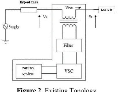
Figure 2.
Existing Topology
In this paper a new topology for DVR based on buck-boost converter has been proposed. The proposed topology is able to compensate any voltage disturbances such as sag, swell and flicker. Unlike the presented topology, the injection transformer is eliminated in the proposed topology. For this reason, the volume and the weight of the proposed topology is impressively reduced. In the first section, the operation principle of the structure is expressed. Then, the implemented control method for the topology is described. Finally, the simulation and experimental results are presented to verify the effective operation of the proposed topology.
II.
PROPOSED TOPOLOGY
The proposed topology for DVR is illustrated in Figure 2. According to the schema, the topology is formed by a conventional buck-boost converter to generate the required compensation voltage in both directions. The structure contains different blocks to regulate the voltage.
Figure 2. Proposed DVR system
They are rectifier, filter, DC-DC converter, microcontroller etc..., the rectifier circuit has convert three phase ac supply into pulsed DC supply. Filter in the block diagram will change that pulsed DC into perfect dc waveform. The DC-DC converter will be used to produce constant DC voltage. The regulated DC voltage can be obtained by varying the PWM pulse given in the DC-DC converter. The microcontroller will control the PWM pulse using input and output feedback voltage. Hence the AC bus has been converted into DC bus with regulated constant voltage. That regulated DC voltage has directly fed into the ac driver for convert into variable AC supply for controlling the speed of the motor load in industries.
topologies are not able to compensate the severe disturbances especially for long time durations. In addition to, this kind of capacitors are heavy and also expensive. Based on the mentioned properties, the proposed DVR can operate in different operation frequency such as dc voltage. Moreover, the long-time disturbances can be compensated by the proposed topology because the required energy is directly provided from the grid. Asmentioned previously, DVR restores the voltage profile by injecting the required voltage.
III. PROPOSED TOPOLOGY DESCRIPTION
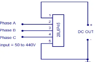
3.1 Three Phase Full BridgeRectifier
Three phase full bridge rectifier circuit is an advanced power rectifier circuit mostly used for industrial DC applications. This module basically has 3 phase inputs and a single DC output. Most of the industrial power supplies such as DC motor drives, welding units, etc. are used these kinds of rectification unit. 3 phase rectifier circuit has been designed using 20L6P45. The circuit diagram for three phase full bridge rectifier has shown in Figure 3.
Figure 3. Circuit diagram for three phase full bridge rectifier
The20L6P45 full wave bridge rectifier module is an advanced 3 Phase silicon diffused type power rectifier which helps to rectify the 3 phase AC input to a single DC output with an efficiency more than 90%. This module can handle maximum power of 20A. This module integrated the basic 3 Phase diode rectification unit itself by the silicon diffusion technology.
The internal structure of 20L6P45 full wave bridge rectifier is shown in the Figure 4. As in the structure, we can see that its internal structure of 20L6P45 is similar to the 3-phase diode bridge rectification unit, But the main advantage is, 20L6P45 chip only taken less space, simpler, less weight, high efficiency, high voltage and current rating, etc.
3.2LC Filter
Figure 5. Circuit diagram for LC Filter
When compared to other type of filters, the π Filter has some advantages like higher dc voltage and smaller ripple factor. But it also has some disadvantages like poor voltage regulation, high peak diode current, and high peak inverse voltage. This filter is divided into two a capacitor filter and a L-section filter. The capacitor C1 does most of the filtering in the circuit and the remaining ripple is removed by the L-section filter (L-C2). C1 is selected to provide very low reactance to the ripple frequency. The voltage regulation is poor for this circuit as the output voltage falls off rapidly with the increase in load current.
3.3 Buck Boost converter
The buck boost converter is a DC to DC converter. The output voltage of the DC to DC converter is less than or greater than the input voltage. The output voltage of the magnitude depends on the duty cycle. These converters are also known as the step-up and step-down transformers and these names are coming from the analogous step-up and step-down transformer. The input voltages are step up/down to some level of more than or less than the input voltage. By using the low conversion energy, the input power is equal to the output power. The circuit diagram for Buck Boost converter as shown in Figure 6.
Figure 6. Circuit diagram for Buck Boost converter
The two-switch buck-boost converter is a cascaded combination of a buck converter followed by a boost converter. Besides therefore mentioned buck-boost mode, where in Q1 and Q2 have identical gate-control signals, the two-switch buck-boost converter
also can operate in either buck or boost mode. By Operating the converter in buck mode when VIN is
higher than VOUT, and in boost mode when VIN is
lower than VOUT, the buck-boost function is then
realized.
3.4 AT89C51 microcontroller
AT89C51 has been used for the proposed technology because of features like high speed, fast response, highly accuracy etc.… The AT89C51 is a low-power, high-performance CMOS 8-bit microcomputer with 4K bytes of Flash programmable and erasable read only memory (PEROM). The device is manufactured using Atmel’s high-density nonvolatile memory technology and iscompatible with the industry-standard MCS-51 instruction set and pinout. The on-chipFlash allows the program memory to be reprogrammed in-system or by a conventional Nonvolatile memory programmer. By Combining a versatile 8-bit CPU With Flash On a monolithic chip, the Atmel AT89C51 Is a powerful microcomputer which provides a highly-flexible and cost-effective solution to many control applications. The pin configuration of AT89C51 is shown in the Figure 7.
Figure 7. Pin configuration of AT89C51
lines, two 16-bit timer/counters, a five-vector two-level interrupt architecture, a full duplex serial port, on-chip oscillator and clock circuitry. In addition, the AT89C51 is designed with static logic for operation down to zero frequency and supports two software selectable power saving modes. The Idle Mode stops the
CPU while allowing the RAM, timer/counters, serial port and interrupt system to continue functioning. The Power-down Mode saves the RAM contents but freezes the oscillator disabling all other chip functions until the next hardware reset.
Pin Description:
VCC : Supply Voltage GND : Ground
Port 0 :it can receive the code bytes during Flash programming, and outputs the code bytes during Program verification. External pullups are required during program verification.
Port 1 :it receives the low-order address bytes during Flash programming and verification
Port 2 : it emits the high-order address byte during fetches from external program memory and during accesses to external data memory that use 16-bit addresses (MOVX @DPTR). In this application, it uses strong internal pullups when emitting 1s. During accesses to external data memory thatuse8-bitaddresses(MOVX@ RI),Port2emitsthecontentsof theP2SpecialFunctionRegister.
Port 3 : It is an 8-bit bi-directional I/O port with internal pullups. The Port 3 output buffers can sink/source four TTL inputs. When 1s are written to Port 3 pins they are pulled high by the internal pullups and can be used as inputs.
RST :Reset input. A high on this pin for two machine cycles while the oscillator is running resets the device.
ALE/PROG: Address Latch Enable output pulse for latching the low byte of the address during accesses to external memory. This pin is also the program pulse input (PROG) during Flash programming.
PSEN :Program Store Enable is the read strobe to external program memory.
EA/VPP: External Access Enable. EA must be strapped to GND in order to enable the device to fetch code from external program memory locations starting at 0000H upto FFFFH.
XTAL1: Input to the inverting oscillator amplifier and input to the internal clock operating circuit.
XTAL2: Output from the inverting oscillator amplifier.
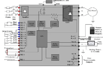
3.5 AC driver
The ac driver will have converting the regulated DC supply into the variable AC supply according to the specification of the motor. V/F converter will be used for the AC driver. The block diagram of the AC driver is shown in Fig.8.
Figure 8. block diagram of the AC driver
3.6 Load
For industries motor has been used as the load for many applications like conveyer, spinning machine, etc.…
4.Modeling and its output
topology, an experimental prototype of this device according to Figure 2 is implemented. The experimental setup will be shown in the Figure 9 The system consists of voltage of 1 pu 50 Hz source as shown in fig with 745kw 3-phase motor load. voltage sag is occurred at 0.5 sec to 1 sec of 0.5 pu and voltage swell occurred of 0.5 pu for 0.2 sec to 0.25 sec.
Figure 10 shows three phase input voltagewaveformsof DVR. As shown figure 11, sag occurs at 0.1sec to 0.15 sec on the any one phase.Hence the voltage from the output of the rectifier will be varied as shown in figure 12. Now the function of Microcontroller would be to inject PWM pulse to the DC-DC Converter has shown in the figure 13, which would result in fairly constant voltage across the load terminal as shown in the figure 14.
Figure 9: experimental setup
Figure 10. three phase input waveforms from the main feeder
Figure 11. wave form of voltage sag occurred in any one phase
Figure 12. waveform of the voltage varied in the output of the rectifier
Figure 13. PWM pulse produced from the Microcontroller
Fig 14: constant voltage present in the DC Grid
IV. CONCLUSION
In this paper a new topology for DVR using microcontroller was proposed. This topology contains rectifier, filter and DC-DC converter. Unlike the conventional topologies, the proposed DVR does not have any injectiontransformer due to the structural features. Because of directconnection to the grid, the storage elements are not required in the proposed topology. Therefore, this topology has less physical volume, mass and price in comparison with traditional topologies. Any kind of voltage disturbances can be compensated by the proposed topology and the effective operation has been confirmed by experimental results.
V.
REFERENCES
[1]. Hietpas, S.M., Naden, M.: 'Automatic voltage regulator using an AC voltage-voltageconverter',IEEETrans.Ind. Appl.,2000, 36,(1), pp. 33–38
[2]. Vilathgamuwa, D.M., Member, S., Perera, A.A.D.R., et al.: 'Dynamic voltage restorer', 2003, 18, (3), pp. 928–936
quality', IEE Proc. Gener.Transm. Distrib.,2003, 150, (5), pp. 513–520
[4]. Wang, B., Member, S., Venkataramanan, G., et al.: 'Operation and control of a dynamic voltage restorer using transformer coupled H-bridge converters', 2006, 21, (4), pp. 1053–1061
[5]. Babaei, E., FarhadiKangarlu, M.: 'Voltage quality improvement by a dynamic voltage restorer based on a direct three-phase converter with fictitious DC link', IET Gener. Transm. Distrib., 2011, 5, (8), p. 814
[6]. Babaei, E., Kangarlu, M.F.: 'Sensitive load voltage compensation against voltage sags/swells and harmonics in the grid voltage and limit downstream fault currents using DVR', Electr. Power Syst. Res., 2012, 83, (1), pp. 80–90
[7]. Jacobson, D.A., Member, S.: 'A novel configuration for a cascade inverter-based storage requirements', IEEE Trans. Power Deliv., 2008, 23, (2), pp.881–888
[8]. Babaei, E.: 'Control of direct three-phase to single-phase converters under balanced and unbalanced operations', Energy Convers. Manag., 2011, 52, (1), pp. 66–74
[9]. Lozano-Garcia, J.M., Ramirez, J.M.: 'Voltage compensator based on a direct matrix converter without energy storage', IET Power Electron., 2015, 8, (3), pp. 321–332
[10]. Babaei, E., FarhadiKangarlu, M.: 'Cross-phase voltage sag compensator for three-phase distribution systems', Int. J. Electr. Power Energy Syst.,2013, 51, pp. 119–126
[11]. Babaei, E., Kangarlu, M.F., Sabahi, M.: 'Compensation of voltage disturbances in distribution systems using single-phase dynamic voltage restorer', Electr. Power Syst. Res., 2010, 80, (12), pp. 1413–1420
[12]. Babaei, E., FarhadiKangarlu, M.: 'Operation and control of dynamic voltage restorer using single-phase direct converter', Energy Convers. Manag., 2011, 52, (8–9), pp. 2965–2972
[13]. Kaniewski, J., Fedyczak, Z., Benysek, G.: 'AC
voltage sag/swell compensator based on