Volume-7 Issue-1
International Journal of Intellectual Advancements
and Research in Engineering Computations
A novel null convention logic (NCL) gates architecture based on basic
gates
Shobika C, Srimalini K, Darani K
Department Of Electronics and Communication Engineering,
Nandha Engineering College, Erode
ABSTRACT
Advanced circlet configuration might interest basic requirements, for example, such that control consumption, robustness, performance, and so on same time continuously executed in VLSI (very la rge scale integration). The non-concurrent standard displays Intriguing features that serve as an elective should these basic Prerequisites a critical population of the non-concurrent standard is those one called QDI (quasi delay insensitive) circuits that could additionally make utilized to discriminating prerequisites plan. QDI circuits would intriguing to these requisitions a result they would hea rty to sure sorts for faults, with clamor also should temperature and supply voltage variations, hosting additionally low electromagnetic outflows an intriguing style about QDI circuits may be the NCL (null gathering logic) circuits since they acknowledge customary. Boolean works and could accomplish incredible streamlining. This paper displays a construction modeling dependent upon essential QDI entryways for those amalgamation for NCL entryways centering for VLSI that employments just standard libraries furthermore FPGA (field programmable entryway array).
Keywords: Non concurrent Logic, QDI Circuits, Dual-Rail Code, FPGA, NCL Entryways.
INTRODUCTION
Computerized frameworks are dominatingly structured dependent on the synchronous world view and customarily have worldwide clock that is in charge of a rhythm of the state change. The fundamental purpose behind this inclination is that the dominant part of existing EDA (Electronic Design Mechanization) streams lead to this worldview. In any case, with the approach of profound sub-micron MOS innovation (DSM-MOS), the synchronous worldview begins to introduce a few issues, for example, a) clock flag dissemination is progressively getting to be troublesome; b) expanding pattern in the variety of the postpone time, bringing about lost execution, in light of the fact that the clock must be set to the most extreme deferral; c) an expanding propensity to clock skew; d) an expansion in clock flag
fan-out > 1 (fork), the postponements ought to be equivalent [3,5]. The correspondence of these circuits with nature is performed in the Info/Output Mode (I/O_M) (eg. DI, SI, QDI) [2,3,5]. In I/O_M, any adjustment in the yield flag can right away empower an adjustment in the information flag. The non concurrent circuit class that better meets the necessities of the MOS-DSM computerized configuration is the QDI class [6]. This class has essential highlights that show to be intriguing, for example, an) a possibility to show better idleness time; b) higher vigor to varieties in temperature, supply voltage and procedure (PVT); c) higher vigor to delay and to Stuck-at flaws (effectively tried blame classes); d) they are profoundly measured, permitting high reusability, and being effectively utilized as licensed innovation - IP [7]; e) a superior execution in security frameworks plan (eg. encryption) [8]; what's more, f) the planning investigation is very improved.
QDI Combinational circuits (QDI_CC) employ m-of-n DI codes to represent data, being the “4-phases” protocol the most common processing.
This paper proposes a novel design for NCL entry ways that works in I/O mode, being QDI (see Fig. 3). The NCL entry ways library, combined by our novel engineering, utilizes as it were essential entryways for the structure, so it very well may be
effectively mapped to FPGA gadgets and to VLSI configuration, in light of on standard libraries. The proposed design pursues the following state condition, which is Z(t+1)=(FNCL-SET +Z(t)).FNCL-RESET.
SYNTHESIS OF NCL GATES
OVERVIEW
Diverse transistor level models have been proposed to execute NCL entryways [13,14]. As instances of a few models that utilization essential doors, we can refer to the proposition of [16,14]. The proposition of [16] depends on the Huffman
machine and the proposition dependent on hook RS that is a semi static CMOS rendition of [14].
Union of NCL doors as Huffman machines
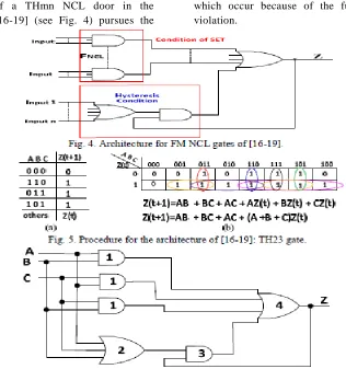
The usage of a THmn NCL door in the engineering of [16-19] (see Fig. 4) pursues the
which occur because of the fundamental mode violation.
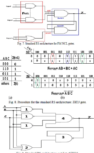
Synthesis of NCL gates as standard RS
The execution of a THmn NCL entryway in the Standard RS design dependent on [14] (see Fig. 7) pursues the traditional extraction of FSET and FRESET capacities. The FSET work is simply the NCL entryway work, supplemented. The FRESET work is the discovery of the n signals going to zero, along these lines being an OR entryway, with fan-in equivalent to n. By representing the
By examining (2), we can have glitches if the imbalance is not fulfilled. As in the engineering of Fig. 4, the glitch in the yield happens in view of the major mode infringement, so the TH23 door isn't QDI.
2xTpMIN-NAND1+TpMIN-NAND4> TpMAX-NAND3 + TpMAX-OR2 (2)
UNION OF QDI NCL GATES
Playing out the planning investigation of the circuit in Fig.10, we have that, expecting An and B going from 0�1 and C=0, the AND1AB door goes 0�1, the OR2 entryway goes 0�1, simultaneously
the Z yield remains 1. The Z yield will possibly go to zero when B goes 1�0, so the TH23 door, executed in the proposed design, complies with the I/O mode and fulfills the QDI defer demonstrate.
SIMULATION AND RESULTS
The plan of the three NCL doors in the three extraordinary designs was done in basic VHDL, and were
aggregated and recreated post-format in ALTER instrument, Quartus II programming, rendition 9.0, Cyclone III family, in EP3C16F484C6 [23] gadget. Figure 10 demonstrate the reproduction post-design of TH23 NCL door. The waveforms show right results for the distinctive tried tasks, following the ones appeared in the task table of Fig. 1a
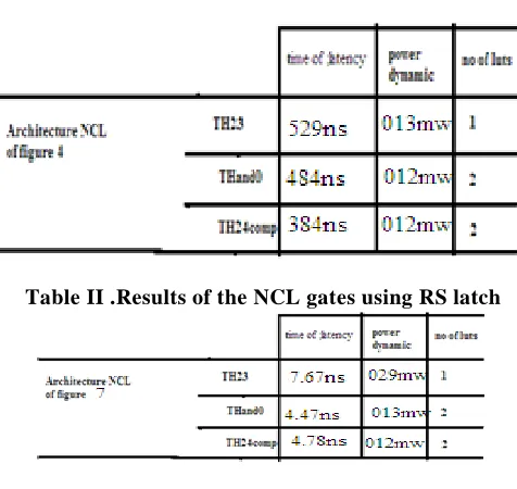
Tables I,II and III demonstrate the outcomes acquired for: I. zone, where just LUTs were utilized; ii. for dynamic power; and iii. for dormancy. The three tables are identified with the usage in the three models of the three NCL entryways. Examining the aftereffects of the three tables, we have: looking at territory, in the case the quantity of LUTs the three models have the same outcomes; looking at dormancy time, the proposed
design got a normal decrease of 8% and 19% at the point when contrasted individually with the designs of Fig. 4 and Fig. 7; looking at the dynamic power utilization, the proposed design acquired a normal decrease, individually, of 38.0% and 28.6% when contrasted with the models of Fig. 4 and Fig. 7. Examining territory (number of CMOS transistors), on account of VLSI execution, the three models acquired similar outcomes.
Table I. Results of the NCL gates using Huffman machine
CONCLUSION
Because of a wide range of utilizations requiring hearty advanced frameworks in the handling or in information security, an intriguing arrangement shows to be the utilization of hearty segments in their amalgamation. In this paper we present a methodology and engineering to blend NCL doors on stages FPGA and standard-cell VLSI. The proposed engineering dependent on fundamental doors actualizes NCL entryways that work in I/O mode and are QDI, while different
structures situated in essential doors produce doors NCL that work in FM mode, so they are not QDI. The proposed NCL doors presents other intriguing properties, for example, high heartiness to varieties in temperature and to supply voltage, which happens all the time in antagonistic conditions, for example, in space and in specific zones of military battle. For further works, it is attractive to test the proposed NCL doors considering radiation impacts of SEU (Single-Event Upset) in FPGA stage [24, 25].
REFERENCES
[1]. B. H. Calhoun, et al., “Digital Circuit Design Challenges and Opportunities in the Era of Nano scale CMOS,” Proc. of the IEEE, 96(2), 2008, 343-365.
[2]. C. J., Myers, “Asynchronous Circuit Design”, Wiley & Sons, Inc, 2a edition 2004.
[3]. P. Beerel, R. Ozdag and M. Ferretti, “A Designer’s Guide to Asynchronous VLSI”. Cambridge University Press, 2010, 337.
[4]. J. Martin, “Compiling Communication to Delay-Insensitive VLSI Circuits”, Distributed Computing, 1(4), 1986, 226-234.
[5]. J. Martin, “The Limitations to Delay Insensitive in Asynchronous Circuits,” 6th MIT Conference on Advanced Research in VLSI Processes,1990, 263-277.
[6]. J. Cortadella, A. Kondratyev, L. Lavagno, and C. Sotiriou, “Coping with the variability of combinational logic delays,” ICCD, 2004, 505– 508.
[7]. W. Hardt, et. al., “Architecture Level Optimization for Asynchronous IPs”, Proc. 13th Annu al IEEE Int. Conf. ASIC/SOC,2000, 158-162.
[8]. L. Spadavecchia, “A Network-based Asynchronous Architecture for Cryptographic Devices,” PhD thesis, University of Edinburgh, 2005.
[9]. C. L. Seitz, “System Timing,” in Introduction to VLSI Systems, Addison -Wesley, 1980, 218-262.
[10].I. David, R. Ginosar, and M. Yoeli, “An Efficient Implementation of Boolean Functions as Self -Timed Circuits,” IEEE Transactions on Computers, Vol. 41(1), 1992, 2-10.
[11].J. Sparsø, J. Staunstrup. “Delay Insensitive Multi Ring Structures”, Integration, the VLSI Journal. 15(13), 1993.
[13].F. A. Parsan and S. C. Smith “CMOS Implementation of Static Threshold Gates with Hysteresis: A New Approach,” In Proceedings of the IFIP/IEEE International Conference on VLSI-SoC, Santa Cruz, CA, USA, 7(10), 2012, 41-45.
[14].F. A. Parsan and S. C. Smith, “CMOS Implementation Comparison of NCL Gates,” In Proceedings of the IEEE International Midwest Symposium on Circuits and Systems, Boise, ID, USA, 5(8), 2012, 394-397. [15].S. C. Smith, et al., “Optimization of NULL convention self-timed circuits,” INTEGRATION, the VLSI
journal 37, 2004, 135–165.
[16].V. Satagopan, et al., “DFT Techniques and Automation for Asynchronous NULL Conventional Logic Circuits,” IEEE Trans. On Very Large Scale Integration (VLSI), vol. 15(10), 2007, 115-1159.
[17].W. K. Al-Assadi and S. Kakarla, “Testing of Asynchronous NULL Conventional Logic (NCL) Circuits in Synchronous-Based Designs,” 22nd IEEE International Symposium on Defect and Fau lt Tolerance in VLSI Systems, 2007, 215-222.
[18].W. K. Al-Assadi and S. Kakarla, “Design for Test of Asynchronous NULL Convention Logic (NCL) Circuits,” IEEE International Test Conference, 2008, 1-8.
[19].L. Duc Tran, et al., “Null Convention Logic (NCL) based Asynchronous Design – Fundamentals and Recent Advances,” International Conference on Recent Advances in Signal Processing, Telecommunications & Computing (SigTelCom), 2017, 158-163.
[20].S. C. Smith, “Design of an FPGA Logic Element for Implementing Asynchronous NULL Convention Logic Circuits,” IEEE Transactions on Very Large Scale Integration (VLSI) Systems, vol. 15 (6), 2007, 672-683.
[21].M. M. Kim, et al., “Design Techniques for NCL-based Asynchronous Circuits on Commercial FPGA,” 17th Euromicro Conference on Digital System Design,2014, 451-458.
[22].J. Cheoljoo and S. Nowick. “Technology mapping and cell merger or asynchronous threshold networks,” IEEE Trans. on Computer-Aided Design of Integrated Circ. and Systems, 27(4), 2008, 659-672.