A FOUR-STAGE POWER AND AREA EFFICIENT OTA WITH 30× (400pF – 12nF) CAPACITIVE LOAD DRIVE RANGE
A Thesis by
SAMUEL ANNOR FORDJOUR
Submitted to the Office of Graduate and Professional Studies of Texas A&M University
in partial fulfillment of the requirements for the degree of MASTER OF SCIENCE
Chair of Committee, Edgar Sánchez-Sinencio Committee Members, Samuel Palermo
Bryan Rasmussen Garng M. Huang Head of Department, Miroslav M. Begovic
December 2016
Major Subject: Electrical Engineering
ABSTRACT
Multistage operational transconductance amplifier (OTA) has been a major research focus as a solution to high DC Gain high Gain Bandwidth and wide voltage swing re-quirement on sub-micron devices. These system rere-quirements, in addition to ultra-large capacitive load drivability (nF-range load capacitor), are useful in applications including LCD drivers, low dropout (LDO) linear regulators, headphone drivers, etc. The major drawback of multistage OTAs is the stability concerns since each added stage introduces low frequency poles. Numerous compensation schemes for three stage OTAs have been proposed in the past decade with only a few four stage OTA in literature.
The proposed design is a four stage OTA which uses an active zero block (AZB) to provide left half plane (LHP) zero to help with phase degradation. AZB is embedded in the second stage ensuring reuse of existing block hence providing area and power savings. This design also uses single miller capacitor in the outer loop which ensures improved speed performance with minimal area overhead. A very reliable slew helper is imple-mented in this design to help with the large signal performance. The slew helper is only operational in the events slewing and does not affect the small signal performance.
The proposed design achieves a DC gain of 114 dB, GBW > 1.77M Hz and PM > 46.9◦ for capacitive load ranging from 400pF–12nF (30×) which is the highest recorded range in literature for these type of compensation. It does this by consuming a total power of143.5µW and an area of0.007mm2
DEDICATION
ACKNOWLEDGMENTS
Firstly, I would like to thank my advisor, Dr. Edgar Sánchez-Sinencio, for his guidance and supervision through out my master’s program in Texas A&M University. I also want to thank my thesis committee members, Dr. Samuel Palermo, Dr. Bryan Rasmussen and Dr. Garng M. Huang, for their time and support.
I would also want to thank my colleagues especially Joseph Samy Riad, who helped me immensely in my research, providing comments and answers when needed. I also want to extend my gratitude to the department faculty and staff for making my time at Texas A&M University a wonderful experience. I am very grateful to Texas Instruments for supporting and financing my tuition in graduate school.
Finally, I must express my very profound gratitude to my family for providing me with unfailing support and continuous encouragement throughout my years of study and through the process of researching and writing this thesis. This accomplishment would not have been possible without them. Thank you.
TABLE OF CONTENTS Page ABSTRACT . . . ii DEDICATION . . . iii ACKNOWLEDGMENTS . . . iv TABLE OF CONTENTS . . . v
LIST OF FIGURES . . . vii
LIST OF TABLES . . . x 1. INTRODUCTION . . . 1 1.1 Motivation . . . 1 1.2 Thesis Organization . . . 2 2. LITERATURE REVIEW . . . 4 2.1 Introduction . . . 4
2.2 Feedback Control Theory . . . 4
2.3 Stability of Feedback System . . . 8
2.4 Various Compensation . . . 11
2.4.1 Dominant Pole Compensation (DPC) . . . 12
2.4.2 Shunt Capacitance (SCC) . . . 14
2.4.3 Miller Capacitor Compensation(MCC) . . . 16
2.4.4 Pole Zero Compensation (PZC) . . . 17
2.4.5 Feedforward Compensation . . . 18
2.5 Existing Op Amp Compensation . . . 20
2.5.1 Compensation Schemes: Three Stage OTA . . . 20
2.5.2 Compensation Schemes: Four Stage OTA . . . 26
3. PROPOSED DESIGN . . . 31
3.1 Principle of Operation . . . 31
3.2 Transfer Function . . . 32
3.3.1 Small Signal Performance . . . 35
3.3.2 Large Signal Performance . . . 35
3.4 Design Procedure . . . 36
3.5 Circuit Implementation . . . 38
3.6 Simulation Results . . . 43
3.6.1 Small Signal Performance . . . 43
3.6.2 Large Signal Performance . . . 45
3.6.3 Monte Carlo and Corner simulation . . . 47
3.6.4 Table of Comparison . . . 49
4. DESIGN TRADE-OFF . . . 51
4.1 Linearity . . . 52
4.2 Noise . . . 55
4.3 Stability . . . 58
4.4 Power Consumption Estimate . . . 59
5. SUMMARY AND CONCLUSIONS . . . 65
REFERENCES . . . 66
APPENDIX A. RATE OF CLOSURE (ROC) . . . 71
APPENDIX B. MILLER EFFECT . . . 73
APPENDIX C. LOCAL FEEDBACK LOOP ANALYSIS . . . 75
APPENDIX D. LAYOUT . . . 77
LIST OF FIGURES
FIGURE Page
2.1 Basic feedback system block diagram . . . 4
2.2 (a) Open-loop characteristics (VTC and gain aϵ) (b) Response of vo to triangular inputvE. Reprinted from [1] . . . 7
2.3 (a) Closed-loop characteristics (VTC and gain A= β1 = 10 ) (b) Inputvi undistorted outputvoand predistorted error signalvE. Reprinted from [1] 8 2.4 Bode plot with GM and PM . . . 10
2.5 External compensation strategies. Reprinted from [1] . . . 12
2.6 Frequency response of various external compensation strategies Reprinted from [1] . . . 13
2.7 Amplifier with dominant pole compensation Reprinted from [1] . . . 14
2.8 Magnitude response showing dominant pole compensation . . . 14
2.9 Amplifier with shunt capacitance compensation Reprinted from [1] . . . . 15
2.10 Magnitude response showing shunt capacitor compensation . . . 15
2.11 Amplifier with miller capacitor compensation Reprinted from [1] . . . 16
2.12 P-Z map illustrating miller compensation . . . 17
2.13 Magnitude response showing miller capacitor compensation . . . 17
2.14 Amplifier with PZ compensation Reprinted from [1] . . . 18
2.15 P-Z map illustrating pole-zero compensation . . . 18
2.16 Magnitude response showing pole-zero compensation . . . 19
2.17 Amplifier with feedforward compensation Reprinted from [1] . . . 19
2.19 Three stage OTA:Compensation with a single miller capacitor . . . 28
2.20 Three stage OTA:Complex compensation . . . 29
2.21 Four stage OTA:Compensation schemes . . . 29
3.1 Block diagram of proposed design . . . 32
3.2 LFL magnitude response of proposed design . . . 37
3.3 Schematics of proposed amplifier core . . . 39
3.4 Block diagram of slew helper . . . 40
3.5 Circuit implementation of slew helper . . . 40
3.6 Working principle of Slew helper in chargingCL . . . 41
3.7 Working principle of Slew helper in dischargingCL . . . 41
3.8 Frequency response of proposed design @ 400pF capacitive load . . . 44
3.9 Frequency response of proposed design @ 12nF capacitive load . . . 44
3.10 Frequency response of proposed design @ 15nF capacitive load . . . 45
3.11 PM and GBW variation with load capacitance . . . 45
3.12 Transient response of proposed design @ 400pF load . . . 46
3.13 Transient response of proposed design @ 12nF load . . . 47
3.14 Transient response of proposed design @ 15nF load . . . 47
4.1 Analog design octagon Reprinted from [2] . . . 51
4.2 (a) Common source amplifier (b) Common source amplifier with resistive degeneration . . . 52
4.3 Closed loop transient response with 300mV amplitude . . . 53
4.4 DFT performed on the transient response . . . 53
4.5 Variation of THD with input signal amplitude in unity feedback . . . 54
4.6 Variation of THD with input pair width. Constants : Ibias = 4µA, Vamp = 300mV . . . 55
4.7 Noise source of transistor . . . 56 4.8 Equivalent input referred noise. ConstantsIbias = 4µA, w= 1.8µm . . . 58 4.9 Variation equivalent input referred noise @ 300kHz with input pair width.
ConstantIbias = 4µA . . . 59 4.10 Variation equivalent input referred noise @ 4.5MHz with input pair width.
ConstantIbias = 4µA . . . 60 4.11 Variation of PM and GM with input pair width. Constant:Ibias = 4µA
CL = 400pF . . . 60 4.12 Variation of PM and GM with input pair width. Constant:Ibias = 4µA
CL = 12nF . . . 61 4.13 Power consumption estimation for different load Constants:Vov andωo . . 63
LIST OF TABLES
TABLE Page
3.1 Parameter values . . . 42
3.2 Transistor sizing . . . 42
3.3 Post-layout simulation summary . . . 46
3.4 Monte carlo simulation @ 12nF load, N=100 . . . 48
3.5 Corner simulation for 12nF load @27oC . . . 48
3.6 Performance comparison with 3 stage OTAs . . . 49
1. INTRODUCTION
1.1 Motivation
Operational Transconductance Amplifier (OTA) is an essential building block in ana-log circuit design. OTAs with ultra large capacitive loads find applications in LCD drivers [3], low-dropout (LDO) linear regulators [4], headphone drivers [5], sample-and-hold am-plifier circuits [6], driving cables with load capacitances in the nF range [7] etc. High DC gain, wide Gain-Bandwidth (GBW) product and large output swing are defining marks of high performance OTAs. Complementary metal-oxide semiconductor (CMOS) technol-ogy nodes has seen remarkable scaling of lower feature sizes in recent years. This trend results in improvement in speed and lower power consumption for digital logic but posing a challenging design consideration for analogue design.
The expression for a short channel MOS transition frequency (fT) and intrinsic gain (gmro) are given in Equation 1.1 and 1.2 obtained from [8]
fT ∝ VEB L (1.1) gmro ∝ L VEB (1.2) whereVEB, L, gm andro are the excess bias voltage (overdrive voltage), channel length, transconductance and output impedance respectively.
From Equ. 1.1, reduction in the feature size of the CMOS results in higherfT and hence faster transistor, however Equ. 1.2 shows reduction in the open loop gain. To improve the reliability of sub-micron devices the VDD scales with minimum feature size. However, in order to have control over the sub-threshold leakage current, threshold voltage
(VT H) don’t scale by the same factor [9]. All these culminates to reduced DC Gain and reduced output swing affecting the very parameters we care for in high performance OTAs. Multistage OTA is a viable option to counteract these effects since cascoding is not possible because of reduced voltage headroom. However each added cascade stage intro-duces a low frequency pole, in which case a suitable compensation scheme is needed to ensure the stability of the system. Designing a compensation scheme is relatively easy for a fixed load, no matter how large. However, designing for a range of load proves to be challenging for reasons that; at low end of the load the stability is limited by the gain margin requirement whiles the phase margin place restriction the largest load that can be driven [3].
Three stage OTAs have been an active research area this past decade providing perfor-mance enhancement for large capacitive load drive.Four stage OTAs have gained research interest recently and has been shown to provide similar or even better performance as the three stage counterpart with less power consumption [10]. The additional transconduc-tance stage relax the requirement of the various gm blocks and provide extra degree of freedom. This added benefit of the forth transconductance stage is exploited and a new topology is proposed.
1.2 Thesis Organization
The 1st chapter introduces the background.
The 2nd chapter describes the concept of frequency compensation. Existing compensa-tion schemes for both three stages and four stages are reviewed and motivacompensa-tion for proposed design is derived.
The 3rd chapter details the proposed design with transfer function and design procedure. Simulation results validating the proposed design is also given
The 4th Chapter explains the various design trade off of the proposed design.
The 5th Chapter issues the discussions and gives the summary.
The Appendix contains some less-interesting but still significant details. Appendix A explains ROC and its significance, Appendix B talks about the concept of miller multiplication, Appendix C explains Local Feedback Loop analysis as a means of comparing the effectiveness of various topologies in light of load range, Appendix D shows proposed design layout and Appendix E, some results from Monte Carlo simulation of the proposed design.
2. LITERATURE REVIEW
2.1 Introduction
Feedback system is ubiquitous and has various applications. It is mainly grouped un-der Positive andNegative Feedback systems with the Negative Feedback Systemfinding most widely used application in electronics and control following Black’s invention of the Negative Feedback Amplifier [11]. Negative feedback system has numerous application benefits which includes gain stabilization, reduction of nonlinearity, impedance transfor-mation (both input and output) and bandwidth enhancement. However feedback systems suffer from the potential of being unstable if not designed properly. This chapter explains the fundamental of feedback control system, stability requirement and discussion of exit-ing frequency compensation of OTA as an application of feedback system.
2.2 Feedback Control Theory
The basic block diagram of negative feedback control system is shown in Figure 2.1. It has a direct path (forward) gain denoted by G(s) and feedback gain, H(s). Also X(s) andY(s)serves as the input and output of the block diagram withE(s), the feedback error, being the difference between the input,X(s)and the fed-back outputY(s)H(s).
The following procedure can be followed to obtain the transfer function fromX(s)to
Y(s)
E(s) =X(s)−H(s)Y(s) (2.1)
Y(s) =G(s)E(s) =G(s)[X(s)−H(s)Y(s)] (2.2)
From Equ. 2.2, the transfer function, XY((ss)), is given by Y(s)
X(s) =
G(s)
1 +H(s)G(s) (2.3)
Equ. 2.3 is called the closed-loop transfer function, so called because the output is sensed and fed-back to the input (forming a closed-loop) to control the system response. The feedback, in this case the negative feedback, works by minimizing the feedback error function, Equ. 2.1, in such a way that the output become a replica of the input. Another important notation is the Loop Gain, L(s) given in Equation 2.5.
The feedback system in Figure 2.1 can be applied to OTA in feedback with G(s) repre-senting the open loop gain, A(s) of OTA and H(s) the feedback factor mostly denoted by βwhich may or may not be frequency dependent. The benefits for connecting OTA in this configuration can not be overemphasized. Using the open loop gain A(s) and feedback factorβ, the closed loop transfer function similar to that in Equ. 2.3 is obtained as shown below with Y(s) and X(s) respectively denoted asVoutandVin.
Vout Vin
= A(s)
1 +βA(s) (2.4)
Open loop gain of OTA are mostly sensitive to process, voltage and temperature (PVT) variations and hence not accurately defined. Desensitization to these open loop effects is provided through negative feedback.
Vout Vin = A 1 +βA = 1 β ( 1 + 1 1 +βA ) ≈ 1 β (2.6)
From Equ.2.6, the closed loop gain to the first approximation is given by β1 which is in-dependent of A(s) and hence PVT assuming that the loop gain,βA≫1. Gain sensitivity function is defined by Equ. 2.7 which is inversely proportional to the amount of feedback (1+L(s)). SACL A = δACL δA A ACL = 1 1 +βA (2.7) ∆ACL ACL =SACL A ∆A A = 1 1 +βA ∆A A (2.8)
Equ. 2.8 shows the application of the sensitivity function showing that variation in the open loop gain is reduced by the amount of feedback and hence the closed loop gain is desensitized from the open loop gain variations [1].
The transfer curve (plot of output against input) of amplifier in open loop has sigmoid shape and the open loop gain variation with respect to the input, Vin, is bell-shaped with the highest gain in the vicinity where Vin=0. As Vin moves away from this vicinity the gain drops creating non-linear effect and finally saturating to the supply rails as shown in Fig.2.2. Non-linearity can be defined as the change in the small signal gain of a system (in this the amplifier) as the input dc level is varied. To avoid this non-linearity and distortion, the negative feedback subtract a fed-back output from the input creating a predistorted error function. This works to linearized the closed loop and evident in Fig. 2.3
Figure 2.2: (a) Open-loop characteristics (VTC and gain aϵ) (b) Response ofvo to trian-gular inputvE. Reprinted from [1]
loop system has been extended to wider input range for the closed loop case. The negative feedback has linearized the system. Analysis of feedback on nonlinearity is extensively treated in [8, 2]
Negative Feedback also helps in extending the bandwidth of the amplifier. Assuming that A(s) is modelled as single pole system, the transfer function is given by
A(s) = Ao 1 + ωs
o
(2.9) whereAo andωo are the low frequency gain and the 3-dB bandwidth respectively. With this definition for A(s), the closed loop transfer function can be expressed as
Vout Vin = Ao 1+ωos 1 + βAo 1+ωos = Ao 1+βAo 1 + s (1+βAo)ωo (2.10) Comparing the 2.9 and 2.10, it can be seen that the closed loop 3-dB bandwidth has been extended by the amount of feedback (1 +βAo). It can also be seen that the gain has
Figure 2.3: (a) Closed-loop characteristics (VTC and gain A= β1 = 10 ) (b) Input vi undistorted outputvo and predistorted error signalvE. Reprinted from [1]
been reduced by the same amount and as a results the gain bandwidth is constant for both open and closed loop system.
2.3 Stability of Feedback System
It is important to note that the transfer function derivation is based complex numbers and hence has magnitude and direction. Despite the numerous advantages of feedback system, there is a risk of instability if care is note taking in its design. Negative feedback works on the principle reduction of error function between the input and fedback output. However there is a delay between when the output is sensed and finally subtracted from the input to generate the error function. This delay may results in overcompensation of the input error resulting in regenerative effect causing the error function to diverge and hence drive the system unstable.
Considering Equ. 2.4, repeated below for emphasis Vout Vin = A 1 +βA = 1 β ( 1 + 1 1 +βA )
whenβA(s = jw) = −1, Vout
Vin = 1/0 = ∞resulting in instability. Under this condition the circuit amplifies its own noise until it eventually begins to oscillate. This condition is defined formally below
|βA(jw)|= 1 (2.11)
̸ βA(jw) = 180◦ (2.12)
and are called the "Barkhausen’s Criteria". The criteria state that oscillation occurs at a frequency ω when a total phase shift of 360◦ is travelled around the loop and at a gain greater than or equal to 1. Since negative feedback accounts for 180◦ phase of the total 360◦ phase required for oscillation, the signal is left with additional180◦ phase shift for oscillation to occur if the gain≥1 hence the criteria.
From another perspective, stability can be determined by inspecting the denominator of the closed loop transfer function and observing if the real parts of the roots are negative or positive. The system is stable if the real parts of roots of closed loop denominator, called poles of the closed loop system, are negative [12].
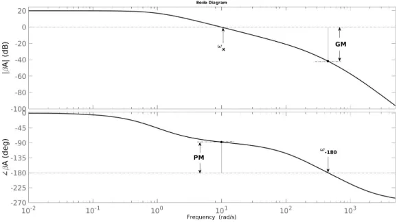
This may suggest the determination of closed loop poles to establish stability but closed loop transfer function is not always readily available. An alternative way is to determine the stability from the open loop transfer function and there are existing tools to do this. One the numerous ways is using Stability Margins to determine stability. Phase Margin (PM) and Gain Margin (GM) form the stability margins.
Phase Margin is the amount degrees by which̸ βA(jωx)can be reduced until it reaches -180◦. Crossover frequency, ωx, is the frequency at which the open loop gain becomes
Figure 2.4: Bode plot with GM and PM
unity or 0 dB. The mathematical expression of PM is given below in Equ. 2.13
P M = 180◦+̸ βA(jωx) (2.13)
Though a positive number for phase margin means the system is stability, to ensure accept-able transient response, that is a system with less overshoot and sufficient settling time, a PM >45◦is required [13].
Gain Margin (GM) on the other hand is referenced toω−180which is the frequency at which the phase crosses −180◦. It is the inverse of the gain measured at a frequency of ω−180ie it is the amount, the gain at |βA(jω−180)|can be reduced until it reaches 0 dB. It is mathematically expressed dB as GM = 20log ( 1 |βA(jω−180)| ) (2.14)
Like the PM, a positive GM is required for stability and can be seen on Figure 2.4. PM most especially has a direct relationship to the overshoot, settling time, rise time etc in second order system. Its effect can not be directly seen for higher order system, however they are still used as a measure of the effectiveness of OTA compensation. This approach will be followed as we discuss the various exiting OTA compensation in the next section.
2.4 Various Compensation
The condition for stability as stated above requires that the total cumulated phase around the loop be ̸ L(jωx) ≤ −180◦. Frequency compensation is modifying the loop transfer function L(s) in such a way to provide adequate phase margin. From Equation 2.5 L(s) = β(s)A(s), one can say that frequency compensation can be achieved by
• modifying the feedback factorβ(s)which leads to external frequency compensation • modifying the open loop transfer function A(s), which leads to internal frequency
compensation
• modifying bothβ(s)and A(s)
External compensation which includes loop gain reduction, input-lag compensation, feedback-lead compensation etc is usually done to change the amplifier characteristics at the application level [1]. Figures 2.5 and 2.6 show respectively the various external compensation strategies and their frequency response. Internal compensation strategy on the other hand is concerned with modifying the amplifier characteristics at the integrated circuit (IC) level and will be the focus of this review.
Modification of the open loop characteristics is done so as to ensure that even in the worse case frequency independent feedback (β = 1), the system remains stable. Internal frequency compensation is broadly grouped under 5 headings, namely:
(a) Loop gain reduction (b) Input-lag compensation
(c) Feedback lead compensation
Figure 2.5: External compensation strategies. Reprinted from [1]
1. Dominant Pole Compensation 2. Shunt Capacitance Compensation 3. Miller Compensation 4. Pole-Zero Compensation
5. Feedforward Compensation
2.4.1 Dominant Pole Compensation (DPC)
Under this compensation scheme, the poles of the uncompensated amplifier are not altered. Compensation is achieved by creating additional pole at a low enough frequency such that it becomes the dominant pole and produces -20 dB/dec roll-off until the crossover frequency (fx). This ensures that the rate of closure (ROC) given by Equation 2.15 is≤30 dB which implies PM ≥ 45◦. The relationship between ROC and PM is elaborated in Appendix A
ROC =| 1 β(jfx)
(a) Loop gain reduction response (b) Input-lag response
(c) Feedback lead response
Figure 2.6: Frequency response of various external compensation strategies Reprinted from [1] TDP C = ao (1 +s/f1)(1 +s/f2)(1 +s/f3)(1 +s/f4) (2.16) wherefi ≈ 2πR1 iCi, i=1, 2, 3, 4 andfD =f4.
Dominant Pole Compensation does not use any of the exiting poles but introduce an-other pole shown in Figure 2.7 which limits the bandwidth of the system. The approximate transfer function of the system is given by Equation 2.16. The highest achievable gain
bandwidth is the dominant pole (f1) of the uncompensated system which is mostly low. Figure 2.8 illustrate the compensation and the gain bandwidth limitation.
Figure 2.7: Amplifier with dominant pole compensation Reprinted from [1]
Figure 2.8: Magnitude response showing dominant pole compensation
2.4.2 Shunt Capacitance (SCC)
Unlike the DPC, shunt capacitance compensation (SCC) uses the system’s exiting poles by rearranging these poles to ensure an ROC of ≤ 30dB. It does this through Cc which pushes the first pole to lower enough frequency as shown in Figure 2.9. Equation 2.17 is the transfer function of the system shown in Figure 2.9.
Figure 2.9: Amplifier with shunt capacitance compensation Reprinted from [1] TSCC = ao (1 +s/fD)(1 +s/f2)(1 +s/f3) (2.17) wherefi ≈ 2πR1iCi, i=2, 3 andfD ≈ 2πR1(C11+Cc).
The highest gain bandwidth product that can be obtained isf2 which is mostly larger thatf1 ie higher GBW can be obtained in this case than in the DPC case. The capacitor Cc required for compensation is mostly big and may not suitable for monolithic IC de-sign because of area constraint. Figure 2.10 shows the compensation using SCC and the movement of the poles.
2.4.3 Miller Capacitor Compensation(MCC)
This compensation strategy shown in Figure 2.11 uses the miller multiplication of capacitor (explained in Appendix B) to implement compensation using smaller capacitor value hence saving area. It ensures pole-splitting pushing the dominant pole to lower frequency and the non-dominant pole to higher frequency for increasing compensation capacitorCc.
Figure 2.11: Amplifier with miller capacitor compensation Reprinted from [1]
Miller capacitor compensation (MCC) is one of the widely used compensation scheme in monolithic IC because it achieves pole splitting, shown in Figure 2.12, with minimum capacitor which saves area. It however, creates a non-minimum phase zero (RHP zero) because of the alternative feedforward path it provides for signal to flow to the output through Cc. There exit numerous techniques to combat this effect and still harness its benefits. These techniques will be touched on in a later section. Figure 2.13 shows the magnitude response and the gain bandwidth limitation of miller capacitor compensation. It can be seen that GBW is limited by f3 which is higher than f2 hence MCC has the highest achievable GBW in comparison to SCC and DPC.
(a) Before miller compensation (b) After miller compensation
Figure 2.12: P-Z map illustrating miller compensation
Figure 2.13: Magnitude response showing miller capacitor compensation
2.4.4 Pole Zero Compensation (PZC)
Pole Zero Compensation (PZC) is a variant of SCC where a capacitor in series with resistor, illustrated in Figure 2.14, is used instead of just a shunt capacitor. Rc ≪ R1 and Cc ≫C1 ensures that the first dominant pole is pushed to a sufficiently low frequency so as to obtained anROC ≤30dB ensuring stability.
In addition to this PZC create a zero to cancel the first non-dominant pole f2 such that f3 becomes the first non-dominant pole after compensation. It can be seen that the
Figure 2.14: Amplifier with PZ compensation Reprinted from [1]
maximum achievable GBW is f3 which is mostly greater than f2. The p-z map of the system, before and after PZC is illustrated in Figure 2.15. Also Figure 2.16 shows the magnitude response and the GBW limitation of system with pole-zero compensation.
(a) Before pole-zero compensation (b) After pole-zero compensation
Figure 2.15: P-Z map illustrating pole-zero compensation
2.4.5 Feedforward Compensation
Under this compensation scheme, a feedforward bypass is provided around the speed bottleneck path. This ensures that slow path is avoid at high frequency to increase the speed of the system. The feedforward path is mostly implemented shown in Equ.2.19 as
Figure 2.16: Magnitude response showing pole-zero compensation
a high pass attenuating the signal at low frequency but passing it at high frequency. From Figure 2.17 one can write input-output transfer function as Equ.2.18
Vo Vin = (a1(s) +hf f(s))a2 (2.18) hf f = jf /fo 1 +jf /fo (2.19)
Figure 2.17: Amplifier with feedforward compensation Reprinted from [1]
At low frequency|hf f(s)| ≪ |a1(s)|henceVo/Vin = a1(s)a2(s) = a(s). This shows that the high gain at low frequency for the uncompensated amplifier is not degraded. At
high frequency |hf f(s)| ≈ 1 ≫ |a1(s)| hence Vo/Vin ≈ a2(s). This proves that the systems dynamics at high frequency is solely controlled by a2 and the slow path a1 is avoided.
The feedforward path can also be implemented with a transconductance stage. Numer-ous benefits including RHP zero compensation, pole-zero cancellation and improvement in large signal performance can be obtained by using a single transconductance stage as feedforward path.
2.5 Existing Op Amp Compensation
Under this section we look at existing amplifier compensations, which include, as we will see a combination of the above internal frequency compensation strategies. This sections looks at the various three-stage and four-stage OTA compensation schemes.
2.5.1 Compensation Schemes: Three Stage OTA
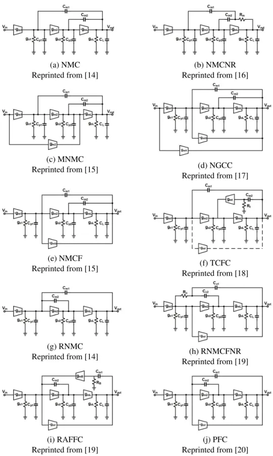
Compensation schemes for three-stage OTAs has been a well-developed research area. There exist numerous schemes and for the purpose of this thesis will be grouped under three main headings.
Compensation with two miller capacitor
The direct application of miller compensation to three stages results in a famous com-pensation scheme called nested miller comcom-pensation (NMC) [14] shown in Figure 2.18a. From the transfer function of NMC given in Equation 2.20, there two zeros associated with this configuration, a left half plane (LHP) zero and a right half plane (RHP) zero. The zeros are assumed to be at higher frequency and hence do not affect the stability. This assumption requires pumping more current to push these zeros out of the frequency of
interest. Av,N M C = gm1gm2gmLRo1Ro2RoL ( 1−sCm2 gmL −s 2Cm1Cm2 gm2gmL ) (1 +sCm1gm2gmLRo1Ro2RL) [ 1 +sCm2(gmL−gm2) gm2gmL +s 2CLCm2 gm2gmL ] ≈ gm1gm2gmLRo1Ro2RoL (1 +sCm1gm2gmLRo1Ro2RL) ( 1 +sCm2 gm2 +s 2CLCm2 gm2gmL ) (2.20)
The most common design procedure involves the assumption of unity feedback and using butterworth condition as elaborated in [15]. According to [15], the internal compensation capacitor limits the speed of the system. Also the sizes of the compensation capacitors are comparable toCLhence not suitable for large capacitive loads.
There are variants of NMC so implemented to improve its short comings. To avoid the RHP zero of NMC which is due to the feedforward path for the small signal, nested miller with nulling resistance (NMCNR) is implemented [16]. As shown in Figure 2.18b ,the resistor, Rm, increases the forward path impedance reducing the feedforward signal and hence pushing the RHP to higher frequency. The RHP zero can altogether be eliminated by ensuring thatRm = 1/gmL as can be seen from the transfer function in Equation 2.21. The PM is increased because of the LHP left after the elimination of the RHP.
Av,N M CN R= gm1gm2gmLRo1Ro2RoL 1 +sCm1gm2gmLRo1Ro2RL × 1 +s [ Cm1Rm+Cm2 ( Rm−g1 mL )] +s2Cm1Cm2(gmLRm−1) gm2gmL 1 +sCm2(gmL−gm2) gm2gmL +s 2 (1−gm2Rm)CLCm2 gm2gmL ≈ gm1gm2gmLRo1Ro2RoL ( 1 +sCm1 gmL ) (1 +sCm1gm2gmLRo1Ro2RL) [ 1 +sCm2(gmL−gm2) gm2gmL +s 2 (1−gm2Rm)CLCm2 gm2gmL ] (2.21) Multipath nested miller compensation (MNMC)[15] uses a feedforward
transconduc-tance to create a low frequency zero to cancel the first non-dominant pole so as to increase both GBW and PM. As shown in Figure 2.18c,gmf1 is sized so as to eliminate the second pole. Though the pole-zero cancellation is within the band of interested it was shown in [15], to be stable for different condition ofCLand gmL hence it is stable under dynamic conditions at the output. The transfer function is given in Equation 2.22 from which the condition ofgmf1is given (Equation 2.23) and elaborated in [15]
Av,M N M C = gm1gm2gmLRo1Ro2RL ( 1 +sCm1gmf1 gm1gm2 ) (1 +sCm1gm2gmLRo1Ro2RL) ( 1 +sCm2 gm2 +s 2CLCm2 gm2gmL ) (2.22) gmf1 = 4.45gm2 (2.23)
NGCC (shown in Figure 2.18d) introduced by You et al[17] has a compact transfer function and hence compact design procedure than any of the above schemes. It ensures that the feed forward signal through the various compensation capacitors are eliminated by a feedforward transconductance. By settinggmf i =gmi, the circuit reduces to a non-zero system similar to NMC without requiring the gmL ≫ gm1, gm2 condition. The transfer function is given in Equation 2.24. A variant of NGCC called NMC with feedforward Gm stage (NMCF) [15] shown in Figure 2.18e takes advantage of LHP zero to improve the PM. The transfer function of NMCF is given by Equation 2.25 with kg = gm2/gmL and m = (gmf2/gm2) > 1. The condition on mis necessary to ensure LHP poles and hence stability of the system.
Av,N GCC,3 = gm1gm2gmLRo1Ro2RL [ 1 +sCm2(gmf2−gm2) gm2gmL +s 2Cm1Cm2(gmf1−gm1) gm1gm2gmL ] (1 +sCm1gm2gmLRo1Ro2RL) [ 1 +sCm2(gmf2−gm2+gmL) gm2gmL +s 2CLCm2 gm2gmL ] = gm1gm2gmLRo1Ro2RL (1 +sCm1gm2gmLRo1Ro2RL) [ 1 +s Cm2 gm2gmL +s 2CLCm2 gm2gmL ] (2.24) Av,N M CF = gm1gm2gmLRo1Ro2RL [ 1 +sCm2(gm−1) mL −s 2Cm1Cm2 gm2gmL ] (1 +sCm1gm2gmLRo1Ro2RL) [ 1 +sCm2(gmf2−gm2+gmL) gm2gmL +s 2CLCm2 gm2gmL ] (2.25) Transconductance with capacitance feedback compensation, TCFC [18] is another variant of NMC where a current buffer is added to the innermost loop capacitor as shown in Figure 2.18f. This has the advantage of preventing the feedforward small signal and hence blocking RHP zero. It has additional feedforward transconductance which helps with large signal performance.
Another compensation scheme using two miller compensation capacitors is reverse nested miller compensation (RNMC)[14]. As shown in Figure 2.18g, this compensation scheme differs from NMC primarily by the internal loop. RNMC does not suffer speed degradation because the internal compensation capacitorCm2 does not load the output ca-pacitor. RNMC feedforward with nulling resistor (RNMCFNR) and Reversed active feed-back frequency compensation (RAFFC) [19] are variants of RNMC as shown in Figure 2.18h and 2.18i respectively, with enhanced performance and also power and area savings. Also RAFFC has the added advantage of no extra circuitry as proposed by [19]. Positive feedback compensation (PFC)[20] is topologically similar to RNMC with the only differ-ence being the polarity of the second and third transconductance stages as shown in Figure 2.18j. The second stage form a positive feedback withCm2which provides damping factor control for complex poles.
Compensation with no inner miller capacitor
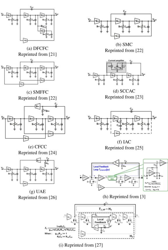
Though RNMC and its variant improves the speed by reducing the output loading by the inner capacitor, the presence of two capacitors for compensation increases the area especially for large capacitive loads. To further improve the speed and reduce the area for large loads, the innermost capacitor is removed and various means are provided to control the damping factor in the following compensation schemes.
Damping factor control frequency compensation (DFCFC) [21] as said earlier removes the inner capacitor and with damping factor control block made up of a transconductance and a feedback capacitor, controls the damping factor of the complex pole. This helps prevent peaking in the frequency response. Large signal improvement is ensured by a push-pull effect throughgmf2as shown in Figure 2.19a.
Single miller capacitor (SMC) and single miller capacitor with feedforward compensa-tion (SMFFC) [22] uses feedforward transconductances (one in SMC and two in SMFFC) to improve system performance shown respectively in Figures 2.19b and 2.19c. SMC uses pole-zero cancellation for improved system performance and in addition to this, SMFFC adds LHP improving the PM of the system.
To prevent the RHP zero and to reduce the compensation capacitance saving the area overhead, a variant of SMC without the feedforward transconductance and with current amplifier in the feedback path is proposed as shown in Figure 2.19d. This scheme called single capacitor with current amplification compensation (SCCAC)[23] has recorded load range of about20×in literature.
Cross feedforward cascode compensation (CFCC)[24] is topologically same as SMFFC with the only different being the cascode compensation shown in Figure 2.19e. The cas-code compensation which is miller compensation with current buffer prevents the RHP zero due to feedforward signal throughCm
remov-ing the inner capacitance, a passive LHP zero is introduce to improve system perfor-mance. This compensation scheme called impedance adapting compensation (IAC)[25] has increased bandwidth with this added zero. A variant of IAC called ultra area-efficient (UAE)[26] amplifier has all the benefits of IAC with an added benefit of area savings. Also the position of passive zero block which is a resistor in series with a capacitor is at the out-put of the first stage not at the second stage as in IAC. The current buffer in feedback path help eliminate the RHP zero in the system. Figures 2.19f and 2.19g show compensation schemes IAC and UAE respectively.
The authors of [3] proposed a compensation which similar to UAE with the only differ-ence being how the LHP zero is generated. In the case of [3], LHP zero is created from an active zero generation block shown in Figure 2.19h. The author of [3] uses local feedback loop (LFL) analysis and realized that the added passive zero block in addition to creating a LHP zero creates a low frequency pole with limits theωµof the local feedback loop of IAC [25]. An active zero generation block does not have this effect and hence ensures extension of the load range of the amplifier (15×).
The author of [27] introduces a buffer between the active zero block of [3] to further prevent the limit on theωµprovided by the active block. The active zero generation block provides a heavy savings on area with minimal/no power overhead when blocks are reused. This compensation scheme is shown in Figure 2.19i
Compensation with complex compensation
This section comprises compensation schemes that involve combination of already exiting schemes.
Dual active capacitive feedback compensation (DACFC)[28] uses only one capacitor with two buffers feedback to the output of the first and second stages as shown in Figure 2.20a. It is similar to CFCC and because of the single capacitor prevents the output stage loading by the inner capacitor which in effect improve the speed performance. The buffers
help in the elimination of RHP zero of the system saving power and ensuring improved system performance.
Dual loop parallel compensation (DLPC)[29] combines the benefits of DFCFC in con-trolling the damping factor and cascode miller compensation which eliminate the RHP zero in a single amplifier as shown in Figure 2.20b. This results in an increased unity gain frequency.
Active feedback frequency compensation (AFFC) [30] has two basic blocks, a high gain block and a high speed block. The high speed block provides an alternate path to skip slow high gain block. The high speed block is composed of cascode miller compensation. This helps to increase the bandwidth. AC boosting compensation (ACBC)[31] is similar to AFFC in the sense that an alternate path is provided to curb the gain reduction of the second stage at high frequency. This alternate path called a high frequency gain stage is wrapped around the second stage and help to extend the unity bandwidth. AFFC and ACBC are shown in Figure 2.20c and 2.20d respectively.
2.5.2 Compensation Schemes: Four Stage OTA
Four stage OTAs have been an active research area recently. The compensation scheme can be traced back to application of three stage compensation schemes on four stages. The initial assumption that the added stage increases power consumption and complicates the compensation scheme has been refuted as some compensation schemes have comparable or even lower power consumption with comparable or better results as their three stage counterpart. Also the added stage can serve to provide extra degree of freedom to realize various performance parameters cared about.
[32] is a four stage OTA using two miller compensation with nulling resistor shown in 2.21a. Two zeros generated are placed in such a way to help with the phase degradation. The system has improved performance but at the expense of power consumption. The
(a) NMC Reprinted from [14] (b) NMCNR Reprinted from [16] (c) MNMC Reprinted from [15] (d) NGCC Reprinted from [17] (e) NMCF Reprinted from [15] (f) TCFC Reprinted from [18] (g) RNMC Reprinted from [14] (h) RNMCFNR Reprinted from [19] (i) RAFFC Reprinted from [19] (j) PFC Reprinted from [20]
(a) DFCFC Reprinted from [21] (b) SMC Reprinted from [22] (c) SMFFC Reprinted from [22] (d) SCCAC Reprinted from [23] (e) CFCC Reprinted from [24] (f) IAC Reprinted from [25] (g) UAE
Reprinted from [26] (h) Reprinted from [3]
(i) Reprinted from [27]
(a) DACFC Reprinted from [28] (b) DLPC Reprinted from [29] (c) AFFC Reprinted from [30] (d) ACBC Reprinted from [31]
Figure 2.20: Three stage OTA:Complex compensation
(a) Reprinted from [32] (b) Reprinted from [33]
(c) Reprinted from [10] (d) Reprinted from [34]
presence of two resistor increases the noise of the system.
Impedance adapting compensation (IAC) scheme is applied to four stage OTA in [34], [10] and [33]. [10] and [34] has cascode miller compensation which help eliminate RHP zero in the system. Also according to Figure 2.21c [10] has only one passive zero gener-ation block at the output of the third stage whiles [34] has two passive genergener-ation blocks at the output of second and third stages as shown in Figure 2.21d. Like [10], the authors of [33] uses a single passive zero generation block at same location and a simple miller compensation in the outermost loop as can be seen in Figure 2.21b. [33] uses feedforward transconductance stages to help improve system performance by ensuring 2 pole-zero can-cellation in addition to the passive zero generated. Also the large signal performance is enhanced through second feedforward transconductance.
The effectiveness of the passive zero generation block in these four stage OTA influ-enced the proposed design which uses a single compensation capacitor and active zero generation block similar to [3] in a four stage OTA.
3. PROPOSED DESIGN
As the number gain stages increases, only one form of internal compensation becomes insufficient to provide the required stability margins for acceptable transient response and as a results a combination of the various internal compensation technique is used. In this chapter a four stage OTA with wide capacitive load drive is proposed. The proposed OTA uses miller compensation and active LHP zero compensation, which is similar to pole-zero compensation, to compensate the OTA over a wide range of capacitive loads. A slew rate helper is used to enhanced the slew performance of OTA with minimal power overhead. The transfer function and design procedure is given in this chapter elaborating the advantage of this design over the already existing techniques.
3.1 Principle of Operation
The block diagram of proposed design is shown Figure 3.1. As can be seen, there are five transconductances, namely;gm1,gma, gmb, gm3 andgm4, in the forward path withgma andgmbimplementinggm2and effectively giving a four stage OTA. Parasitic conductances and capacitances per stage is denoted by goi andCpi respectively where i=1, b, 3, 4. goz andCpz are the parasitics of the active zero LHP generation block. As stated in previous chapter, the care about of amplifiers are the gain, speed, area and power consumption. The gain of the OTA is given by the product of per stage transconductance and conductance ratios as shown is Figure 3.1.
Each added gain stage introduce a low frequency pole which poses stability issues. The stability of proposed OTA is ensured throughCm which implements miller compensation and an active LHP zero block implemented withgmz,RzandCz. The miller capacitor,Cm, ensures pole splitting pushing the dominant pole to a lower enough frequency to ensure single pole characteristics until the crossover frequency. The interaction between high
Figure 3.1: Block diagram of proposed design
frequency pole due to miller compensation and the second non-dominant pole creates a high-Q complex pole. This is suppress by the zero created by the active zero generation block. With this zero carefully placed, the phase degradation by the complex pole is compensated giving an acceptable PM and hence a good transient response. To help with the large signal response, an optional feed-forward transconductance,gmf, can be used.
3.2 Transfer Function
The transfer function of the proposed design is obtained based on the following as-sumptions;
• CL≫Cm> Cz ≫Cpiwhere i=1,..,4,z and b=2 • gmi
goi ≫1wheregm2 =
gmagmb
gmz , i=1,..,4,z and b=2
The detailed transfer function using the above conditions is given in Equation 3.1.
H(s) = b0+b1s+b2s 2+b
3s3+b4s4+b5s5 a0+a1s+a2s2 +a3s3+a4s4+a5s5+a6s6
where a0 = go1go3go4gobgmz Rz b0 = gm1gm3gm4gmagmb Rz a1 = Cmgm3gm4gmagmb Rz b1 =Czgm1gm3gm4gmagmb a2 =CmCzgm3gm4gmagmb b2 =− CmCzgm1go3gob Rz a3 = CLCmCzgo3gob Rz b3 =− CmCzCpbgm1go3 Rz a4 = CLCmCzCpb Rz b4 =−CmCzCpbCp3gm1 Rz a5 = CLCmCzCpbCp3 Rz b5 =−CmCzCpbCp3Cpzgm1 a6 =CLCmCzCpbCp3Cpz (3.2)
The above transfer function, Equation 3.1, can be expressed in factored form as given in Equation 3.3 by using the approach in [35].
H(s) = Adc[(1 + 1 ωz1s)(1 + 1 ωz2s)(1 + 1 ωz3s)(1 + 1 ωz4s)(1 + 1 ωz5s)] (1 + ω1 3dBs)(1 + 1 ωoQs+ 1 ω2 os 2)(1 + 1 ωp3s)(1 + 1 ωp4s)(1 + 1 ωp5s) (3.3) where Adc = gm1gm3gm4gmagmb go1go3go4gobgmz ω3dB = go1go3go4gobgmz Cmgm3gm4gmagmb ωz1 = 1 RzCz ωoQ= 1 RzCz −ωz2 = gm3gm4gmagmbRz Cmgo3gob ωo2 = gm3gm4gmagmb CLCzgo3gob ωz3 = gob Cpb ωp3 = gob Cpb ωz4 = go3 Cp3 ωp4 = go3 Cp3 ωz5 = 1 RzCpz ωp5 = 1 RzCpz (3.4)
From the detailed transfer function in factored form, we obtain a simplified transfer function by observing that ωz(3−5) = ωp(3−5) resulting in pole zero cancellation at very
high frequency, outside the band of interest. It can be noted that imperfections in the pole-zero cancellation does not affect system performance as they are way outside the band of interest. Also the non-minimum phase zero (RHP) ωz2 is at high enough frequency and hence ignored in the simplified transfer function given in Equation 3.5 with the terms having similar definitions as that of the detailed transfer function in factored form given in Equation 3.4 H(s) = Adc(1 + 1 ωz1s) (1 + ω1 3dBs)(1 + 1 ωoQs+ 1 ω2 os 2) (3.5)
From the simplified transfer function Equation 3.5, it can be seen that the somewhat com-plex transfer function reduces to a simple form which enhances circuit analysis and per-formance tracking.
The phase margin of the proposed system is given in Equation 3.6. Improvement in the phase performance byωz1can clearly be seen is this equation.
P M =180◦−arctan ( GBW w3dB ) −arctan GBW wo Q [ 1− ( GBW wo )2] +arctan ( GBW wz1 ) =90◦−arctan GBW wo Q [ 1− ( GBW wo )2] +arctan ( GBW ωz1 ) (3.6) Similarly, GBW of the proposed design is given by Equation 3.7 which follows the general GBW of multistage amplifiers.
GBW =Adc×ω3dB ≈ gm1 Cm
3.3 Circuit Performance
The circuit performance can be broadly placed under two groups, namely small signal performance and large signal performance.
3.3.1 Small Signal Performance
The small signal performance is mainly characterized by the GBW and the stability margins, PM and GM of the system. The simplified transfer function was obtained un-der small signal conditions. The DC gain given by Adc in Equation 3.4 shows that the gain term is contributed by an additional transconductance gm4 which increases the gain in comparison to the other 3 stage counterpart [3]. Also for the same DC gain, the addi-tional gm stage reduces the individual gm’s required in the 3 stages OTA which effectively reduces the current consumption assuming the same overdrive in both cases.
From Equation 3.6, the effect of the active zero can clearly be seen. The design steps start by setting the GBW given in Equation 3.7 and placingωo > GBW. According to Equation 3.4, ωo depends on gma, gmb, gm3 and gm4 which can be optimized to place ωo for a given power and a particular capacitive load, CL and PM. Also theωz1 is placed in the vicinity ofωoso as to reduce the phase degradation by the complex pole. Czshould be set so as to not pushωoto close to GBW and at the same time sized well to create zero to prevent the phase degradation. The flexibility in placing the zero is then achieved through Rzwhich may affect the noise performance and also the range of load drive.
3.3.2 Large Signal Performance
The main large signal specification is slew rate which is defined as the maximum rate of change of the output voltage with respect to time. As said earlier,gmf is implemented optionally to help in the large signal performance of the OTA and hence has little or no influence on the small signal performance. gmf forms a push-pull with the main input
transistor of the fourth stage, gm4, mimicking a class AB effect. The slew rate (SR) is given by Equation 3.8 which, due to the class AB effect provided bygmf, is limited byCm for low enough capacitive load. However for capacitive loads in the nF-range, the SR is mostly limited byCLand hence the output stage.
SR ≈min ( I1 Cm , I4 CL ) (3.8) The simplest way to improve SR is to increase the output load current. This however increases the power consumption of the proposed design, hence a slew helper was imple-mented to improve the SR performance of the system. This is will elaborated in a later section (Section 3.5).
3.4 Design Procedure
Local feedback loop analysis (explained in Appendix C) is applied to the proposed design and loop transfer function is given in Equation 3.9 and it magnitude plot is shown in Figure 3.2. From the LFL of the proposed design, there is control over how omegaµ, ωz1and the limiting poleω3are placed, hence its effective in its ability to drive wide range as explained in Appendix C. TLF L=− gmagmbgm3gm4 gmzgo1gobgo3go4 sCm(1 + ωs z1) (1 + ωs 1)(1 + s ω2)(1 + s ω3)(1 + s ω4)(1 + s ω5)(1 + s ω6) (3.9) ω1 = go4 CL ω2 = go1 Cm ω3 = gmz Cz ω4 = gob Cpb ω5 = go3 Cp3 ω6 = 1 RzCpz LG= gmagmbgm3gm4 gmzgo1gobgo3 Cm CL ωµ= gmagmbgm3gm4 gmzgo1gobgo3 Cm CL ωz1 = 1 RzCz (3.10)
Figure 3.2: LFL magnitude response of proposed design
From the simplified transfer function Equation 3.5, the LFL transfer function Equation 3.9, the equations for PM (Equation 3.6) and GBW (Equation 3.7), the design procedure is given below. Note that this procedure is done with the assumption that the GBW, power consumption, noise level and other important circuit are known priori.
• Determinegm1to satisfy noise requirement and random offset • From the particular GBW andgm1,Cmis determined
• Ensure thatωµ> GBW at large loads and alsoωµ< ω3at low loads
• For a good phase margin, say> 45◦, placeωo >GBW.ωo are placed at 2×GBW for PM=45◦
be used to cancel the limiting pole of LFL which will help extendωµ. However, this will results in a minimal PM improvement by LHP zeroωz1 in amplifier’s response • To save area and also help with LFL’s PM at low load,ωz1 ≈3×GBW and placed
beforeω3 of LFL shown in Figure 3.2 (ieωz1 ≈GBW< ω3)
• ChoosingRz > 1/gmz ensures placingωz1 of the LFL before LFL’sω3 hence im-proving PM in the LFL at low loads
• From Equation 3.4ωo ∝ √C1
L hence the above condition can be achieved with low power for low loads
• The design is optimized for the largest load
• The 4th-stage provide extra degree of freedom and hence low gm can be used saving power and area.
• ωo has an extragm which means it is easier to situate it where you want in this case 2×GBW with less power
3.5 Circuit Implementation
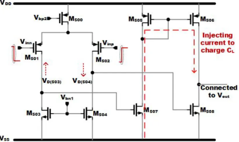
The circuit implementation is shown in Figure 3.3 and is implemented in IBM 130nm CMOS process. The first stage is implemented withM100−108 whereM100 is the biasing transistor. M201−204 implements the second stage with the active zero generation block, composed of Rz, Cz and gmz, embedded in the second stage to save power. gmz is im-plemented with M202, gma andgmb withM201 and M204 respectively. The third stage is implemented withM301−304 and the fourth stage with M401−402. The feedforwardgmf is implemented withM401andgm4 withM402
As stated in Section 3.3, a slew rate helper is needed to improve the slewing perfor-mance of amplifier with nF-range loads. A slew helper [36] which has two main parts, the
Figure 3.3: Schematics of proposed amplifier core
detection part which detects the on-set of slewing and SR boosting part which is switched on when the circuit starts slewing was implemented. The block diagram illustrating the slew helper is shown in Figure 3.4. It can clearly be seen from this figure that, the slew boosting path and the main signal path do not interrupts each other during normal opera-tion. The detection block turns one of the two switches on, to either pump current into the output capacitor or sink current from the output capacitor. This results in a faster charging or discharging of the capacitor and hence improvement in slew rate. From Figure 3.5,M501 andM502 serve as the detection part and are connected to the input of the main amplifier core. M503 andM504 act as current source loads to the inputM501andM502and are sized to carry more current than the input pair (i.e. ID(503,504) > ID(501,502)). This condition ensures that the drain voltage ofM503andM504,VD(503)andVD(504) respectively, are low enough to biasM507andM508which serve as the switch of the SR boosting stage in cut-off at nominal operation. M505 andM506 mirrors the current fromM507 to give a symmetric SR boosting independent of whether falling or rising edge of the input is slewing.
At the nominal circuit operation, VD(503) and VD(504) are low, biasing the switches, M507andM508, in cut-off. Assuming a pulse is applied to the input as shown in Figure 3.6,
Figure 3.4: Block diagram of slew helper
VD(503) goes high turning onM507 whilesM508is still off asVD(504)goes down. Through M505andM506, current is injected to the output, charging the output capacitor faster. With a pulse as shown in Figure 3.7 the opposite effect happens. In this caseM508 is turned on drawing current from the output and hence discharging the output capacitor faster.
Figure 3.6: Working principle of Slew helper in chargingCL
This slew helper has minimal power overhead and does not affect the small signal per-formance of the OTA. This improves large signal perper-formance of the system with minimal or no added current consumption. Care must be taking in deciding on how largeID(503,504) should be in comparison toID(501,502) since this affects the voltage step that turns on the switches and hence the SR boosting stage.
Following the design procedure in Section 3.4 and using the schematic shown in Figure 3.3, the parameters and transistor sizes are respectively shown in Table 3.1 and Table 3.2.
Parameter Value Parameter Value
gm1(µS) 32.3 gm4 (µS) 570.8 gma (µS) 103.3 gmf (µS) 796.2 gmb(µS) 117.2 Cm(pF) 2.3 gmz (µS) 102.7 Cz (pF) 0.8 gm3(µS) 201.3 Rz(kΩ) 30
Table 3.1: Parameter values
Transistor W/L (µm/µm) IF Transistor W/L (µm/µm) IF M101,102 4(0.45/0.35) 7 M203 8(0.76/0.4) 9.8 M103,104 2(0.81/0.8) 11 M301 12(0.8/0.5) 12.8 M105,106 2(0.8/0.7) 1.5 M302,304 4(0.5/0.4) 9 M107,108 2(1.07/0.8) 2.8 M303 14(0.76/0.4) 10 M201 10(0.6/0.5) 9.7 M401 32(1.44/0.5) 10 M202,204 2(0.45/0.4) 10 M402 4(0.5/0.2) 24.5 M100 (bias) 8(1.62/1) 5.6
Table 3.2: Transistor sizing
with-out slew helper and one with slew helper is laid with-out. Good laywith-out techniques including common centroid, inter-digitization, guard ringing etc were used ensuring low mismatch effects and reduction in deterministic errors. The layout of both OTA individually and on a padframe is shown in Appendix D.
3.6 Simulation Results
To check both small and large signal performances of the OTA, the following simula-tions were carried using Virtuoso Analog Design Environment with Spectre as the simu-lator. For small signal performance which is mainly the measurement of stability margins, DC Gain and GBW, stb analysis was performed. The large signal performance was done using transient response and the slew rate was measured. DC simulation was performed to measure the power consumption of the OTA.
3.6.1 Small Signal Performance
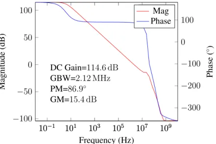
Post layout simulation results obtained from stb analysis performed on the proposed design are given below for 400pF and 12nF loads. Simulation for 15nF is also added to see how the proposed design works at that load (so as to compare with literature).
Figure 3.8 shows the frequency response of the proposed design under 400pF ca-pacitive loading condition. The zero of the active zero generation block can clearly be seen in this response. With CL = 400pF, ωo is pushed to a higher frequency than the zero hence the zero flattens the −20dB/dec slope before the ωo kicks in, resulting in −40dB/decafterωo. The measured stability margins under this condition isP M = 86.9◦ andGM = 15.4dB, withGBW = 2.12M Hz.
Under 12 nF loading condition shown in Figure 3.9 the proposed design shows a well-behaved system with stability margins of P M = 46.9◦ and GM = 13dB. The ωo is within 10 decades of the GBW designed for, (which is 2MHz) hence reducing the GBW to1.77M Hz
10−1 101 103 105 107 109 −100 −50 0 50 100 DC Gain=114.6 dB GBW=2.12 MHz PM=86.9◦ GM=15.4 dB Frequency (Hz) Magnitude (dB) Mag 10−1 101 103 105 107 109 −300 −200 −100 0 100 Phase ( ◦ ) Mag Phase
Figure 3.8: Frequency response of proposed design @ 400pF capacitive load
10−1 101 103 105 107 109 −100 −50 0 50 100 DC Gain=114.6 dB GBW=1.77 MHz PM=46.9◦ GM=13 dB Frequency (Hz) Magnitude (dB) Mag 10−1 101 103 105 107 109 −300 −200 −100 0 100 Phase ( ◦ ) Mag Phase
Figure 3.9: Frequency response of proposed design @ 12nF capacitive load
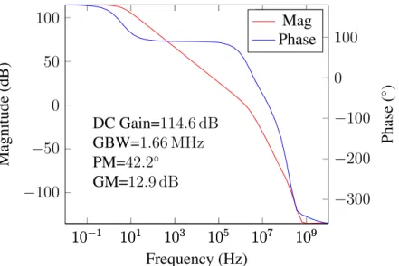
Though the proposed OTA was not design for a capacitive load of 15nF, it can be seen from Figure 3.10 that the system produce acceptable response giving PM and GBW of 42.2◦ and 1.66 MHz respectively (See Table 3.3). The small signal performance under the different load conditions are tabulated in Table 3.3.
10−1 101 103 105 107 109 −100 −50 0 50 100 DC Gain=114.6 dB GBW=1.66 MHz PM=42.2◦ GM=12.9 dB Frequency (Hz) Magnitude (dB) Mag 10−1 101 103 105 107 109 −300 −200 −100 0 100 Phase ( ◦ ) Mag Phase
Figure 3.10: Frequency response of proposed design @ 15nF capacitive load
2 4 6 8 10 12 14 50 60 70 80 CL(nF) P M ( ◦ ) PM 2 4 6 8 10 12 14 1.8 1.9 2 2.1 GB W ( M H z ) PM GBW
Figure 3.11: PM and GBW variation with load capacitance
3.6.2 Large Signal Performance
The transient response under 400pF, 12nF and 15nF loading conditions are given be-low. From Figure 3.13 and 3.14, the improvement by the slew helper can clearly be seen.
400pF 12nF 15nF DC Gain (dB) 114.6 114.6 114.6 IDD (µA) 119.6 119.6 119.6 GM (dB) 15.4 13 12.86 GBW (MHz) 2.12 1.77 1.66 PM (o) 86.9 46.9 42.2 SR(V/µs) 2.66 0.19 0.17
Table 3.3: Post-layout simulation summary
Aside the reduction of the overshoot, the slew helper’s effect is not very obvious in the 400pF loading condition. Unlike other enhancement schemes, this slew helper depends on the input signal themselves to detect slewing and not internal nodes like those in [27]. Also the scheme did not affect small signal response and it worked well across corners evident in Table 3.5 and Appendix E.
0 0.2 0.4 0.6 0.8 1 ·10−4 −0.2 −0.1 0 0.1 0.2 Rise/Fall time=1 ps SR =2.66V/µs SR =1.05V/µs time (s) V oltage (V)
with slew helper without slew helper
Input
0 0.2 0.4 0.6 0.8 1 ·10−4 −0.2 −0.1 0 0.1 0.2 Rise/Fall time=1 ps SR =0.19V/µs SR =0.09V/µs time (s) V oltage (V)
with slew helper without slew helper
Input
Figure 3.13: Transient response of proposed design @ 12nF load
0 0.2 0.4 0.6 0.8 1 ·10−4 −0.2 −0.1 0 0.1 0.2 Rise/Fall time=1 ps SR =0.17V/µs SR =0.07V/µs time (s) V oltage (V)
with slew helper without slew helper
Input
Figure 3.14: Transient response of proposed design @ 15nF load
3.6.3 Monte Carlo and Corner simulation
The summary of Monte Carlo and Corner simulation (details of various simulations are shown in Appendix E).
Mean SD Min @3σ DC Gain (dB) 113.56 1.38 109.42 IDD (µA) 125.3 13.43 85.01 GM (dB) 14.83 1.25 11.08 GBW (MHz) 1.85 0.045 1.72 PM (o) 52.5 2.43 45.21
Table 3.4: Monte carlo simulation @ 12nF load, N=100
From Table 3.4, the minimum performance parameters @ 3σ suggest that at least 99.7% of the yield will have this minimum parameters. This means that mismatches do not affect the design much if good layout techniques are used. Variation of performance
TT FF SS FS SF DC Gain (dB) 113.6 113.4 113.4 112.8 114 IDD (µA) 123.4 129.6 118.4 123.1 123.6 GM (dB) 14.76 16.79 12.95 16.15 13.33 GBW (MHz) 1.86 1.94 1.75 1.75 1.94 PM (o) 52.3 54.4 49.7 54.2 49.4
Table 3.5: Corner simulation for 12nF load @27oC
due to process has been done on the proposed design. From Table 3.5, DC gain records worst perform of 112.8 dB under FS corner, worst GM and GBW were recorded as 12.95 dB and 1.75 MHz respectively under SS corner and worst PM of 49.4 ◦ under SF corner. Even under these corners the proposed design has comparable performances as existing strategies in literature.
3.6.4 Table of Comparison
The performance of the proposed OTA was compared with both 3 stage OTAs (Table 3.6 ) and 4 stage OTAs (Table 3.7 ) in literature. The proposed designed has admirable performance in comparison to existing solution.
Ref Ref Ref Ref Ref This work This work Specifications [22] [18] [37] [25] [3] (no helper) (with helper) Tech (µm) 0.5 0.35 0.35 0.35 0.35 0.13 0.13 CL(pF) 120 150 500 150 15000 12000 12000 Power (mW ) 0.42 0.045 0.225 0.03 0.144 0.146 0.144 IDD(mA ) 0.21 0.03 0.15 0.02 0.072 0.12 0.12 VDD(V) 2 1.5 1.5 1.5 2 1.2 1.2 GBW(MHz) 9 2.85 1.4 4.4 0.95 1.97 1.77 SR(V/µs)@1nF/12nF 0.51 1.04 2 1.8 0.22 0.98/0.09 1.18/0.19 F OMS= GBWP ower×CL 2567 9500 3111 22000 98958 161343 147993 F OML=SRP ower×CL 972 3450 4445 9000 22917 7371 15636 IF OMS= GBWIDD×CL 5134 14250 4667 33000 197916 193612 177591 IF OML= SRIDD×CL 1943 5175 6667 13500 45834 8845 19064 Area (mm2) 0.015 <0.02 0.075 <0.02 0.016 0.006 0.007 CT otal(pF) 4 2.02 50 1.6 2.6 3.1 3.1 Capacitive Load Range 1x 1x 1x 1x 15x 30x 30x
Ref Ref Ref Ref Ref This Work This Work Specifications [38] [39] [17] [32] [10] (no helper) (with helper) Tech(µm) 1.5 0.8 2 0.12 0.35 0.13 0.13 CL(pF) 250 10 20 500 1000 12000 12000 Power (mW ) 10 4.5 0.68 1.4 0.156 0.146 0.144 IDD(mA ) 2 0.3 0.34 1.4 0.052 0.12 0.12 VDD(V) 5 1.5 2 1 3 1.2 1.2 GBW(MHz) 2 6 0.61 40.2 2.98 1.97 1.77 SR(V/µs)@1nF/12nF 1.5 13 2.5 17.52 1.18 0.98/0.09 1.18/0.19 F OMS= GBWP ower×CL 50 133 18 14357 19103 161343 147993 F OML= SRP ower×CL 38 289 74 6257 7564 7371 15636 IF OMS = GBWIDD×CL 250 200 36 14357 57308 193612 177591 IF OML= SRIDD×CL 188 433 147 6257 22692 8845 19064 Area (mm2) 0.625 0.05 0.22 0.017 0.014 0.006 0.007 CT otal(pF) 34.5 4.9 – 17.6 9.7 3.1 3.1 Capacitive Load Range 1x 1x 1x 1x 1x 30x 30x
![Figure 2.6: Frequency response of various external compensation strategies Reprinted from [1]](https://thumb-us.123doks.com/thumbv2/123dok_us/1871022.2773071/23.918.145.800.132.722/figure-frequency-response-various-external-compensation-strategies-reprinted.webp)