(Tehran Polytechnic)
Vol. 46 - No. 2 - Fall 2014, pp. 47- 52 )AIJ-MISC)
٭Corresponding Author, Email: [email protected]
Fully Distributed Modeling, Analysis and Simulation of
an Improved Non-Uniform Traveling Wave Structure
H. Khoshniyat
1, A. Abdipour
1*, and G. Moradi
11- Electrical Engineering Department, Amirkabir University of Technology,Tehran, Iran
ABSTRACT
Modeling and simulation of communication circuits at high frequency are important challenges ahead in
the design and construction of these circuits. Knowing the fact that the lumped element model is not valid at
high frequency, distributed analysis is presented based on active and passive transmission lines theory. In
this paper, a lossy transmission line model of traveling wave switch (TWSW) is presented and fully
distributed analysis of this structure is also introduced. In the off state, the ordinary single pole single throw
(SPST) switches operate as short or open circuit and return an observable part of the signal. To improve
return loss in the off state, a non-uniform structure of SPST switches is proposed which is based on the
artificial tapered transmission line produced by applying various controlling voltage at the gate. The analysis
of ordinary and improved structure of SPST switches is performed and it is further compared with that of the
semi-distributed and fully distributed methods. The results of simulation easily approve the improvement of
matching in the off state.
KEYWORDS
1.INTRODUCTION
Nowadays, the request for millimeter wave
applications such as radar systems and high-speed wireless LAN systems is growing quickly and also there is an enormous demand for microwave circuits to operate at higher and higher frequency to attain greater bandwidths. On the other hand, there has been a huge request for microwave integrated circuit applications at various frequencies caused by having a low fabrication cost and a better operation at higher frequencies.
In communication and radar systems, switches have a fundamental role in controlling the flow of RF signal in both transmitters and receivers. In these applications, wide-band switches with high power transfer capability and switching speed have a major duty in realization of low-cost communication systems.
Given the broad range of applications involving millimeter wave circuits in high speed communications and the fundamental role played by distributed switches in communication systems, there has been an enormous amount of research carried out on several microwave switches to improve switch performance. Toward this end, there has been some research to improve parameters such as insertion loss and isolation. In different millimeter wave applications, various switch structures are reported in the literatures [1]-[8].
In [1], performance of a traveling wave switch is analyzed with a lossy transmission line model. A traveling wave switch using fully distributed FET has been developed and discussed in [2]. In [3], the optimized length of switch is achieved based on scattering parameters graph versus length and frequency. [4] demonstrates a switch structure, which has a shunt structure in connection with a quarter wavelength transformer. The switches designed with this type of structure have isolation greater than 25 dB and an insertion loss less than 1.5 dB in the frequency range from 59 GHz to 61 GHz. Another structure involves a series FET in parallel with an inductor. Such a switch has an isolation of 20 dB and an insertion loss of 1.6 dB at 94 GHz [5]. Yet another switch circuit has the series-shunt structure using the ohmic electrode sharing technology (OEST). Such a switch has an isolation of more than 20.6 dB and an insertion loss of less than 1.64 dB; these structures have been discussed in [6]. In [7] and [8], the improvement of SPST switches was fully discussed by a new structure based on SPST switches and the operating on and off voltages have been also optimized.
In this paper, a lossy transmission line model is demonstrated for modeling of single pole single throw traveling wave switch and fully distributed analysis of this structure is presented by applying the lossy TL model. In the off state, the ordinary SPST switches have a low return loss and behave like a short circuit or open circuit to prevent the transmission of RF signal [3]. The unfavorable VSWR in the off state probably makes some obstacles in RF systems. The reflected signal from the switch may damage the previous segment or disturb the normal behavior of system. In [8], to improve the return loss in the off state, the structure of SPST switches based on the structure of single pole double throw (SPDT) switches and quarter-wave transformers, was proposed. In this research, improvement of the switch behavior in the off state is done based on applying various controlling voltages at the gate that cause the transmission line model of switch becomes non-uniform and tapered. The semi distributed and fully distributed analysis of common and improved structure of SPST switches is performed. To validate the fully distributed method, the results of this method are compared with those of semi-distributed results done with commercial RF softwares which show a good agreement. The results of the improved switch demonstrate good matching of switch and the improvement in return loss in the off state.
2.COMMON STRUCTURE OF SPST SWITCHES
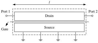
The schematic of a Single Pole Single Throw (SPST) Traveling Wave Switch (TWSW) is illustrated in Fig. 1. By applying the gate voltage (Vg), the transfer of signal through the drain transmission line is controlled. In this structure, the length of the switch is comparable to the wavelength of the maximum frequency of the circuit, therefore the wave transmission in this structure cannot be ignored and no lump model is reliable to analyze a distributed switch. Instead, distributed modeling should be applied for the analysis of these elements [1].
l
Source Drain
Gate
Port 1 Port 2
Fig. 1.The schematic of SPST traveling wave switch
modeling. The sliced model of TWSW is shown in Fig. 2. Using the small-signal transistor model in the off and on states of the switch (Fig. 3) and the drain transmission line model, the lossy transmission line model of switch is attained (Fig. 4).
Fig. 2.The equivalent sliced model of switch
Fig. 3.The small-signal model of transistor
Fig. 4.The lossy transmission line model of switch
The primary parameters of the TL model are represented as [2]:
(
)
(
)
TL TL
TL FET g
FET g
R
R
L
L
C
C
C
V
G
G
V
(1)
The secondary parameters of the TL model, i.e. the propagation constant, γ and charcteristics impedance Z, are given as [2]:
j
R
j L G
j C
(2)
R
j L
Z
G
j C
(3)
In these equations, RTL and LTL are the series resistance and inductance of the drain transmission line per unit length, and C and G are the shunt
capacitance and conductance of the lossy
transmission line per unit length, respectively. The values of C and G are dependent on status of the switch (Vg). The series resistance RTL is considered to be equal to Rac that is proportional to the square of frequency and caused by the skin effect. RTL can be represented by [1]:
TL
R
f
(4)
The lossy transmission line is presented by the ABCD matrix (transmission matrix) as:
cosh
sinh
1
sinh
cosh
l
Z
l
A
B
C
D
l
l
Z
(5)
By converting the ABCD matrix to scattering matrix, the scattering parameters are obtained as [3]:
2 2
0
11 2 2
0 0
sinh
2
cosh
sinh
Z
Z
l
S
ZZ
l
Z
Z
l
(6)
0
21 2 2
0 0
2
2
cosh
sinh
ZZ
S
ZZ
l
Z
Z
l
(7)
Fig. 5.G versus Vg based on the Curtice 2 equivalent model of FET
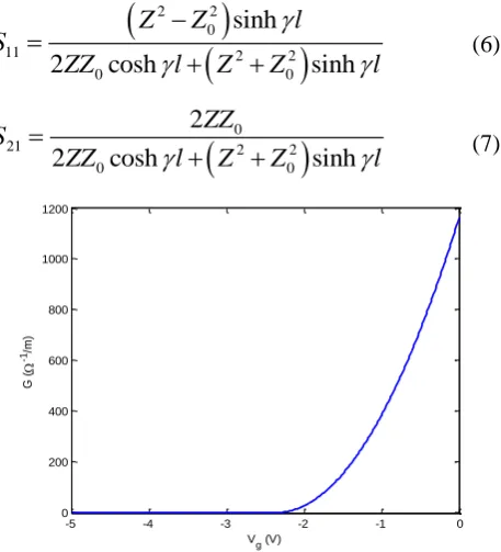
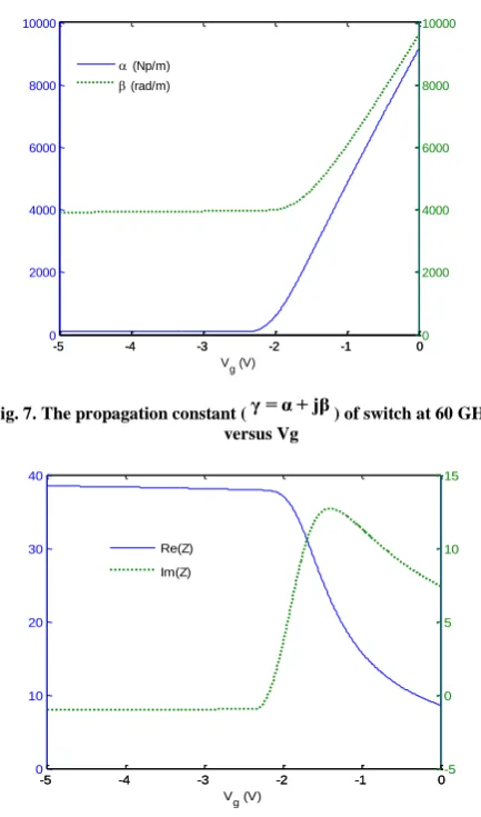
As the values of C and G vary in the on and off states, the secondary parameters γ and Z are changed; thus, the scattering parameters are dependent on the status of the switch. Using the parameter values for 100µm FET, the values of R, L, C and G per unit length are calculated and used in simulations [3]. In Figs. 5-6, C and G are shown as a function of Vg. In Figs. 7-8, the secondary parameters γ and Z are shown at 60 GHz versus Vg.
Vg
Port 1 Port 2
Rg
-5 -4 -3 -2 -1 0
0 200 400 600 800 1000 1200
V
g (V)
G
(
-1/m
Fig. 6.C versus Vg based on the Curtice 2 equivalent model of FET
Fig. 7.The propagation constant (γ = α + jβ) of switch at 60 GHz versus Vg
Fig. 8.The characteristic impedance of switch at 60 GHz versus Vg
3.AN IMPROVED NON-UNIFORM STRUCTURE
In this section, the structure of improved SPST switches is presented and a fully distributed analysis of this structure is introduced based on the transmission matrix. The common SPST switch in the off state, behaves like a short or open circuit and prevents the transfer of signal through the drain transmission line and returns a high ratio of signal. The reflected signal may disturb the performance of system or damage the previous part of the
system. Therefore, the necessity of improvement of this structure is clear.
Improved structure is based on applying different control voltages to each section of gate transmission line. As shown in Fig. 9, by applying control voltage into the middle of gate transmission line and Vgs(on) at its both ends, based on resistive divider, Vg is obtained in each section. If Vgs(on) is applied as the control voltage, Vg will be equal to Vgs(on) in the entire sections of gate line and the behavior of switch is similar to that of the common switch. However, if Vgs(off) is applied as the control voltage, Vg changes gradually from Vgs(on) to Vgs(off) in the gate line and similar to matching load and
tapered transmission line, firstly the wave faces with on-state and propagates in the structure, then in the middle of structure, it encounteres with off-state that a large part of signal is reflected and wasted in transmission line in the return path. Accordingly, by applying various control voltages (Vg) in the gate line, the equivalent circuit of the transistor in each sector is a function of the voltage Vg and by using a non-linear model of transistor, the values of GFET and CFET are calculated for each section.
l
Source Drain
Gate
Port 1 Port 2
( ) 5 ( ) 0
gs
Control gs
V on V V
V off V
1 gs( ) 5
VV on V V2Vgs(on) 5V
Fig. 9.The schematic of improved SPST switch
The Curtice 2 is used for non-linear modeling of transistor that parameters are in [7]. Thus, the transmission line model is non-uniform in the off state. The ABCD matrix of each segment is obtained with assuming that each section is uniform. Then global ABCD matrix is obtained by multiplying them together, and finally the scattering matrix is calculated from it.
cosh
sinh
1
sinh
cosh
i i i
i i
i i
z
Z
z
A
B
z
z
C
D
Z
(8)
1
N
i i
A
B
A
B
C
D
C
D
(9)
-5 -4 -3 -2 -1 0
2.65 2.7 2.75 2.8 2.85 2.9 2.95 3 3.05
3.1x 10
-10
Vg (V)
C
(
F
/m
)
-5 -4 -3 -2 -1 0
0 2000 4000 6000 8000 10000
Vg (V)
-5 -4 -3 -2 -1 00
2000 4000 6000 8000 10000
(Np/m)
(rad/m)
-5 -4 -3 -2 -1 0
0 10 20 30 40
Vg (V)
-5 -4 -3 -2 -1 0-5
0 5 10 15
Re(Z)
Due to the required distribution of voltage in gate line in the off state, the desired resistive distribution can be achieved; the resistive distribution can be modeled as non-uniform gate’s transmission line with losses. Accordingly, the behavior of switch is a function of voltage distribution at gate line and the performance is checked with linear and exponential distribution function.
4.FULLY DISTRIBUTED ANALYSIS
In this section, the fully distributed and semi-distributed analysis of common and improved SPST switches is done. In [3], the method is presented to estimate the optimum length of the common SPST switch, via this method, the 800µm switch is obtained at the operating frequency of 60 GHz. High reflection coefficient in the off state is the main disadvantage of this structure. Therefore, the improved structure is applied to reduce S11(off).
Fig. 10.S11 and S21 of common 800µm switch in the on state.
Fig. 11.S11 and S21 of common 800µm switch
in the off state.
Fig. 12.Linear distribution of voltage at gate transmission line
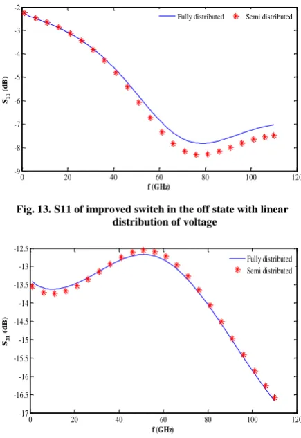
In Figs. 10-14, the analysis results of common and improved SPST switches are shown. The improved structure is analyzed with linear distribution of voltage in gate as shown in Figs. 12-14. The fully distributed analysis is based on the calculation of transmission matrix and converting its elements to scattering parameters. In semi-distributed analysis, the common SPST switch is divided into 40 slices and simulated with commercial software. As seen in these figures, the fully and semi distributed analysis results have a good agreement with each other and the fully distributed method is validated.
Fig. 13.S11 of improved switch in the off state with linear distribution of voltage
Fig. 14.Isolation of improved switch in the off state with linear distribution of voltage
By validation of fully distributed analysis, the behavior of improved structure is studied with an exponential distribution of voltage Vg(x) described as:
0 20 40 60 80 100 120
-100 -80 -60 -40 -20 0
f (GHz) S21
(d
B
)
0 20 40 60 80 100 120-5
0
S11
(d
B
)
0 20 40 60 80 100 120-5
-4 -3 -2 -1 0
0 0.1 0.2 0.3 0.4 0.5 0.6 0.7 0.8 0.9 11
-5 -4 -3 -2 -1 0
x/length Vg
(x
)
0 20 40 60 80 100 120
-9 -8 -7 -6 -5 -4 -3 -2
f (GHz)
S11
(
d
B
)
Fully distributed Semi distributed
0 20 40 60 80 100 120
-17 -16.5 -16 -15.5 -15 -14.5 -14 -13.5 -13 -12.5
f (GHz)
S21
(
d
B
)
(1 )
5
0
0.5
( )
5
0.5
1
x L
x L
x L g
x L
e
V x
e
(10)
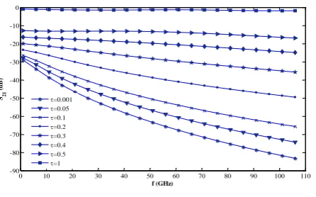
In Figs. 15-16, the analysis results for different values of τ, are shown. For small values (τ =0.001), the improved structure behaves as the common switch in the off state with good isolation while for large values (τ=1), it behave as the common switch in the on state with proper return loss. With middle values (τ =0.2 & 0.3), the tradeoff may happen between isolation and return loss.
Using the improved structure, the reflection coefficient in the off state is reduced and the improvement in the performance of switch will occur (Fig. 15) The structure affects neither the performance of switch in the on state, nor the parameters such as insertion loss or reflection coefficient of the on state while the complexity of realization of voltage distribution network of gate line is one of the greatest difficulties in this structures.
Fig. 15.S11(dB) of improved switch with exponential distribution of voltage with various τ
Fig. 16.S21(dB) of improved switch with exponential distribution of voltage with various τ
5.CONCLUSION
The ordinary SPST switch has a high reflection coefficient in the off state and behaves as a short or open circuit in this case. Therefore, the requirement for improvement of this parameter is becoming obvious. The improved structure of SPST switch was presented based
on non uniform transmission line structures and the fully distributed analysis of this structure and the common structure was done and the improvement in the performance of switch in the off state was indicated. Also, the fully distributed analysis was validated with sliced switch analysis.
REFERENCES
[1] H. Mizutani, and Y. Takayama, ”DC-110-GHz
MMIC traveling waveswitch," IEEE Trans. Microwave Theory Tech., vol. 48, No. 5, pp. 840-845, May, 2000.
[2] H. Mizutani, N. Iwata, Y. Takayama, and K. Honjo, “Design Considerations for Traveling-Wave Single-Pole Multithrow MMIC Switch Using Fully Distributed FET," IEEE Trans. Microwave Theory Tech., vol. 55, No. 4, pp. 664-671, April 2007.
[3] H. Khoshniyat, G. Moradi, A. Abdipour, and K. Afrooz, “Optimization and Fully Distributed Analysis of Traveling Wave Switches at
Millimeter Wave Frequency Band," 1st
MMWATT Conf., pp. 45-49, Dec, 2009.
[4] G. L. Lan, D. L. Dunn, J. C. Chen, C. K. Pao, and D. C. Wang, “A high performance V-band monolithic FET transmit-receive switch," IEEE Microwave Millimeter-Wave Monolithic Circuits Symp. Dig., pp. 99-101, May, 1988.
[5] H. Takasu, F. Sasaki, H. Kawasaki, H. Tokuda, and S. Kamihashi, “W-band SPST transistor switches," IEEE Microwave Guided Wave Lett., vol. 6, pp. 315-316, Sept, 1996.
[6] H. Mizutani, M. Funabashi, M. Kuzuharad, and Y. Takayama, “Compact DC-60 GHz HJFET MMIC
switches using ohmic electrode- sharing
technology," IEEE Trans. Microwave Theory Tech., vol. 46, pp. 1597-1603, Nov. 1998.
[7] H. Khoshniyat, G. Moradi, A. Abdipour, K. Afrooz, "Optimization and Fully-Distributed Analysis of Single-Pole Single-Throw Traveling Wave Switches at Millimeter Wave Frequency Band,” International Journal of Information and Communication Technology (IJICT), vol.3, no.2, pp.19-25, March 2011.
[8] H. Khoshniyat, G. Moradi, A. Abdipour, K. Afrooz, "Fully distributed analysis of an improved single pole single throw traveling wave switches," 21st Iranian Conference on Electrical Engineering (ICEE 2013), pp.1-4, May, 2013.
0 10 20 30 40 50 60 70 80 90 100 110
-30 -25 -20 -15 -10 -5 0
f (GHz)
S11
(
d
B
)
=0.001
=0.05
=0.1
=0.2
=0.3
=0.4
=0.5
=1
0 10 20 30 40 50 60 70 80 90 100 110
-90 -80 -70 -60 -50 -40 -30 -20 -10 0
f (GHz)
S21
(
d
B
)
=0.001
=0.05
=0.1
=0.2
=0.3
=0.4
=0.5