358
358
Copyright © 2016. Vandana Publications. All Rights Reserved.
Volume-7, Issue-1, January-February 2017
International Journal of Engineering and Management Research
Page Number: 358-362
A Detailed Analysis of MSK Modulators and Its Performance
Dr.M.Pushpavalli1, T.Nivetha2, G.Nivashini3
1,2,3Bannari Amman Institute Of Technology Sathyamangalam, Erode, INDIA
ABSTRACT
High speed VLSI circuit design has attracted important attention in the communication industry and academia in the past years as a candidate technology for the transceiver systems. These systems have been developed to support high data rate with high spectral and energy efficiency, low resource utilization and high operation frequency. Hence, MSK modulation technique has been advanced for high spectral efficiency. Therefore, it is of critical importance to carry out efficient MSK transmitter. However, available MSK architectures, although able to achieve transmission data, cannot respond low resource utilization, latency and complexity structures. In this paperwe analyzea FPGA based MSK transmitter, which is more efficient than traditional MSK structure. The transmitter consists of four ROMs, two multiplexer blocks and one adder blocks while conventional MSK architecture has four ROMs, two multipliers and one adder blocks.
I.
INTRODUCTION
In recent years, the telecommunication systems can progressively generate signal with high bandwidth by using high speed hardware. Therefore, VLSI (Very Large Scale Integration) circuit design techniques are widely used in area of communication industry and academia. In especial, some decoder designers are now following a low latency and complexity decoder architectures [1]-[3]. This latency and complexity issue is also significant in modulator and demodulator design. In wireless communication systems, M-PSK (Phase Shift Keying) transmission techniques are very preferred owing to its desirable BER properties and simply hardware architecture. Yet, M-PSK is out of favoured in some areas where spectral efficiency is important. Hence, because of MSK (Minimum Shift Keying) signal's desirable spectral features, it has been attached for wireless communication systems such as satellite
communication [4]. However, MSK modulator
architecture is complicated than M-PSK transmitter because M -PSK scheme can be formed using M number ROMs and 2M to 1 multiplexer blocks while MSK can be consists of either operational blocks (multipliers and adder) or NCO (Numerically Controlled Oscillator) based modulator design [5].
To date, there have been a multitude of research activities on FPGA (Field Programmable Gate Array), VLSI or microwave circuit based MSK Architectures [8], [9], [10]. Specifically, in early years, microwave circuit based MSK transmitter was very popular [4], [8], [9]. In order to use at S-Band, a microwave MAMSK modem, which has important of bandwidth efficiency, was considered in [4]. In another paper, microwave circuit-based MSK modem for satellite communication was proposed using offset biphasekeying technique [9]. Meanwhile, extensive MSK schemes have been designed to increase data rate and bandwidth efficiency by using microwave circuits [4], [8], [9]. In [10], a transmitter that uses FPGA-based architecture instead of microwave circuit was designed. This MSK modulator was implemented using DS-SS (Direct Sequence Spread Spectrum) technique. In order to reduce resource utilization of FPGA, a MSK transmitter structure was proposed using frequency shape pulse of rectangle [5]. Although this method is different to traditional techniques, it has very complex scheme. A FPGA-based transmitter was suggested in information transmission system of radar targets [6]. In this paper, modulator consisted of NCO block that was realized using phase and frequency control words. This NCO framework uses high resource and is complicated build. In paper [7], radar communication waveform was generated for operating at UHF-band.
359
359
Copyright © 2016. Vandana Publications. All Rights Reserved.
model. Subsequently, the simulation results are compared to demonstrate the efficiency of the proposed modulator scheme. Finally, it shows that the proposed model utilizes low-resource and is low-complexity than conventional MSK architecture.
II.
DIGITAL MODULATOR
ARCHITECTURE
2.1. Binary Digital Modulator Structures
Owing to its low complexity, multiplexer- based architectures are one of the most preferred structures for binary modulation methods. According to the level of binary data, desired input signal is activated by using 2 to 1 multiplexer. This binary modulator structure is illustrated in Fig. 1. In this figure, ROMs are utilized for saving of samples of carrier signals. Besides, because of its symbol number, this modulator structure
exerts least ram bits among multiplexer-based
modulators.
In Fig. 2.1.1, BXSK may be presented one of the BASK, BFSK or BPSK signals. This architecture is the most simply algorithm in digital communication systems. For instance, equality of BPSK signal is given following.
SBPSK (t) Accos(2πfc t kπ) (1)
In BPSK expression, k will be 0 when message bit is 1. On the other hand, k will be 1 for 0 message bit. In traditional BPSK modulator, if message bit is directly applied on multiplier block, output signal of BPSK modulator is 0 for 0 message bit. This case is generally called BASK modulator with On-Off Keying technique [11]. In order to obtain BPSK signal by using multipliers, message data is implemented on not-return to zero block and 0 message bit is coded as -1.
SBPSK (t) Accos(2πfc t) for n '1' (2) SBPSK (t) −Accos(2πfc t) for n '0'
In equations (2), n represents message bit logical level. The equation 2 provides binary modulator architecture that is given in Fig. In QPSK modulator architecture, bit number of one symbol consists of two message bit. Therefore, symbol bit number of binary and quadrate transmission techniques is different. So, QPSK modulator utilizes four ROM blocks, and also 4 to 1 multiplexer is operated in the structure.
2.2. MSK Modulator
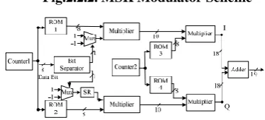
Compared to binary or quadrate modulator architectures, MSK transmitter has more complicated and further utilizes resource. Hence, reducing resource utilization and complexity of this architecture is very important topic. The block scheme of traditional MSK modulator is illustrated in Fig. 2.2.2.
As shown in Fig.2.2.2, M1 and M2 or M3 and M4 layers are serial. Namely, output signals of M1 or M3 are need for computing of output signals of M2 or M4. In
Fig. 2.2.1.Binary Modulator Architecture
order to prevent obtain zero in output of M1 and M3 multipliers, NRZ (not-return to zero) was used as run in
Fig.2.2.2. MSK Modulator Scheme
conventional BPSK modulator. According to this case, FPGA based traditional MSK modulator is given in
Fig.2.2.3. In this figure, SR, which is presented shift
Fig. 2.2.3.FPGA-based traditional MSK modulator
register, is used for providing of half bit period delay. In this figure, bit_separator block is act as serial to parallel de-multiplexer. NRZ block function is created by using multiplexer blocks. According to the output bit of bit_separator, selector pin activates 1 or -1 fixed point number for multiplication of weighting signals.
360
360
Copyright © 2016. Vandana Publications. All Rights Reserved.
Fig.2.2.4. FPGA-based traditional MSK modulatorIII.
PROPOSED MSK
ARCHITECTURE
In order to minimize traditional MSK structure in Fig. 2.2.3, we proposed that pre-computation technique is used for determining of I node and Q node signals which are presented ISMO and QSMO respectively. To achieve this goal, we applied multiplexer based architecture in place of four multipliers blocks. ISMO and QSMO are consist of two distinct signals, phases of which are opposite by 180 degree. We run two different ROMs for each of ISMO and QSMO samples values. In SDR (SoftwareDefined Radio) applications, signal generators aregenerally created by using two different methods: Firsttechnique is
using of ROM blocks while second method
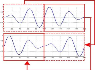
isimplementation of NCO which also acts as ROM. Theresource utilization is very high in the NCO architectures and also their processing time is longer than traditional MSK structures because of design of NCO. If our structure is carefully examined, it can be shown that twoparallel binary modulator architectures are used in thegeneration of I node and Q node signals. As shown in Fig.3.2 and Fig.3.3, peak values of ISMO or QSMO signalschange for different period in one bit period. For example,magnitude values of 100th and 45th samples of red signalare different as shown in Fig3.2. However, in BPSKmodulator, peak values of carrier signals are stable in each period. In our design, ISMO and QSMO is takenaccount as two discrete binary signal. Namely, ISMO maybe any of two signals of which nth time absolute values isequal, and also these signals are the exact opposite ofeach other as shown in Fig. 3.2. Correlation coefficient ofcarrier signals of binary phase modulator and correlationcoefficient of I nodes signals or Q nodes signals are -1 so that I nodes or Q nodes signals demonstrate similarbehavior such as binary phase carrier signals. Therefore, our architecture, which is seen in Fig. 3.1, consists of two parallel binary phase modulator.
Fig.3.1. FPGA-based proposed MSK modulator
In Fig. 3.1, it is used two different counter blocks because of half bit period delay of Q channel. Up to first half bit time, counter 1 increases address line of ROM1 and ROM2 while counter 2 is frozen. Compared with traditional MSK, our scheme has also four ROMs but RAM bit number of our structure are less than traditional MSK architecture as given in compilation report results. If not operator is not applied, this structure wont used with traditional MSK demodulator.
As realized in the BPSK structure, the signal with „o‟ marker in Fig. 3.2 is applied to adder block when 1 message bit is transmitted. If 0 message signal is transmitted, other signal, which is activated on output of multiplexer block, is created I nodes signal. In order to provide this case, first half period of sinus is saved on ROM instead of ISP or QSP signals whichcalled as weight signals [12]. For noiseless medium, bit error rate is 0.5 in this case when traditional demodulator architecture is used in detection. In order to not change bit error rate, we propose following algorithm in modulator architecture.
Algorithm
Input: d _in, Output: i, q Variable: k, y, a, b k=mod(y) if k=1 i<=d_in(a) q<= not d_in(b) end
if k=0
i<= not d_in(a) q<=d_in(b) end
In this algorithm, y is represented as sequence of message bits. The mod operation is used for obtaining even bits of I channel and odd bits of Q channel. Besides, a, b, i, q is described as bit indices, i and q channel bits. With this process, negative samples of ROM1 and ROM2 can be multiplied with I and Q channel bits that are incurred not operator. Therefore, these inverse bits are multiplied with negative alternance of weight signals.
361
361
Copyright © 2016. Vandana Publications. All Rights Reserved.
Fig.3.3. Q node signalFig. 3.4.Proposed MSK modulator scheme-I in Quartus
As shown in Fig. 3.2 and Fig. 3.3, there is 180 degree phase difference between blue signals and red signals. In Fig. 2.2.4, it is shown that phase of signal changes in 0 -1 or 1-0 transitions when it is considered time chart of any of the ISMO or QSMO signals.
We save blue and red signals on ROMs so that, four ROMs are used in our design. FPGA-based MSK architecture is given in Fig. 3.4. In figure 3.4, it can be seen that the transmitter system is designed by using proposed parallel architecture. Normally, MSK scheme with multiplier is applicable using pipeline system however, complexity and latency cycle of conventional MSK structure is higher than our MSK architecture. The samples of I node signals are saved on I_ch_phase1 and phase2. The signals in Fig. 3.3 are placed in Q_ ch_phase1 and phase2. As shown in Fig. 3.4, there was used four ROMs of which address line are 200. Therefore, 200 samples are saved on each ROM. The bit_seperator block, which is used to convert serial data bit to parallel, connects parallel message bits to selector pin of I and Q channel multiplexer blocks. Thanks to this process, the generating of I node or Q node signals are provided with one multiplexer. Therefore, serial connected two multiplier blocks are removed in MSK transmitter architecture. Besides, two multiplexer blocks
in conventional MSK structure are abolished for processing of NRZ.
The half bit period time difference between I channel signal and Q channel signal is ensured using two counters that control address line of ROMs. Further, counter2 block is passive up to first half bit period. However, this counter is removed for resource efficiency. The first message bit and last message bit, which is called Q bit and I bit respectively, can be used as dummy bits in both traditional structure and our architecture. Namely, not only ISMO both also QSMO are applied on adder block while first bit and last bit are transmitting. On account ofthis, resource utilization such as register or logic element can be reduced. In order to provide this aim, we propose to replace technique. This technique is defined that Q channel signal‟s samples are saved whereby a different way. Namely, addresses of
samples in Q_ch_phase1 and phase2 must be change. Therefore, the samples-1, which exist in 0-99 address lines, and the samples which are saved in 100-199 address lines, are exchanged as shown in Fig. 9. In this way, lower resource utilization is provided. This technique wasn't tried in any study.
In Fig. 3.5, it is shown that new sample sequence Q-Ch_Phase1 block by utilizing replace technique. In the same way, the samples in Q_ch_phase2 are saved. This figure looks alike QPSK modulator architecture. The adder block is extra used in MSK structure when the path delay of QPSK and MSK architecture is compared. Additionally, our architecture operates as addition of output signals of parallel two binary modulators. In summary, proposed architecture has lower complexity than traditional MSK transmitter.
362
362
Copyright © 2016. Vandana Publications. All Rights Reserved.
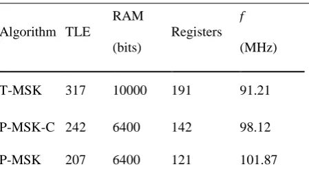
Table 3.1.Compilation ResultsAlgorithm TLE
RAM
Registers f
(bits) (MHz)
T-MSK 317 10000 191 91.21
P-MSK-C 242 6400 142 98.12
P-MSK 207 6400 121 101.87
Fig. 3.6.Simulation results for P-MSK architecture
IV
SIMULATION AND
COMPILATION RESULTS
The entire MSK transmitter architectures were designed using Quartus 9.1sp2. The all simulation and compilation results are given from modelsimaltera simulator and Quartus compiler program, respectively. As explained in the previous section, we used 200 samples for each ROM. Therefore, total ram bit numbers are 6400 because each sample consists of 8 bits. Therefore, multiplication of sample number (200)*ROM number (4)*bit number for each sample (8) makes 6400 bit. However, traditional MSK architecture is used 10000 ram bits as shown in Table 3.1.
T-MSK, P-MSK-C and P-MSK are represented traditional MSK, proposed MSK with two counters and proposed MSK with one counter, respectively. P-MSK-C architecture is shown in Fig. 3.1. The two different
counters were used for I_ ch_phase1-2 and
Q_ch_phase1-2. However, this architecture has lower complexity traditional MSK structure. Further, this architecture utilizes lower resource. Yet, it is shown that the proposed structure in Fig. 8 is the most efficiency transmitter architecture. P-MSK is used lower TLE (Total Logic Element) and register than P-MSK- C and T-MSK although its ram bit number is equal to MSK-C. In Fig. 3.6, it is shown that simulation results of P-MSK. I nodes and Q nodes signals are represented I_mux and q_mux in Fig. 3.6, respectively. As shown in this figure, MSK signal was successfully achieved. It is shown that the proposed replace technique succeeds as shown in Fig. 3.5, if first half period of MSK and q_ mux signals is carefully examined. Compared with the replaced signal in Fig. 3.5, first half bit period of q_mux is equal to that signal.
V.
CONCLUSION
In this paper, a different MSK modulator scheme is proposed. Based on this scheme, a low complexity MSK transmitter is presented. In addition, with the use of replace approach, resource utilization of MSK transmitter is further reduced. Compilation shows that the proposed MSK architectures have important
advantages with respect to both complexity and hardware efficiency. In this brief, this modulator architecture is tried the first time in this paper. In this manner, the replace technique wasn't applied on any MSK transmitter architecture.
REFERENCES
[1] Z., Chuan, and K. K. Parhi, “Low-latency sequential and overlapped architectures for successive cancellation polar decoder” IEEE Transactions on Signal Processing, vol. 61, pp: 2429-2441, May. 2013.
[2] B. Yuan and K. Parhi, “Low-latency successive-cancellation list decoders for polar codes with multibit decision,” IEEE Transactions on Very Large Scale Integration (VLSI) Systems, vol. PP, no. 99, pp. 1–13, 2014.
[3] C. Zhang, B. Yuan, and K. K. Parhi, “Reduced-latency SC polar decoder architectures,” in Proc. IEEE Int. Conf. Commun. (ICC), pp. 3471–3475, Jun. 2012.
[4] W.J.Weber, P.H.Stanton, and J.T.Sumida,“A
bandwidth compressive modulation system using multiamplitude minimum shift keying (MAMSK),”IEEE Trans. Commun., vol. 26, no. 5, pp. 543–551, May. 1978.
[5] X. Bu, W. Meng, “A New Modulation
Implementation Method of the CPM,” 2011 International Conference of Information Technology, Computer Engineering and Management Sciences, pp.152-155, Sept. 2011
[6] W. Xie, and D. Heng, “Design and verification of MSK based on FPGA,” International Conference on Measurement, Information and Control (ICMIC), pp. 486-489, Jun. 2013.
[7] Z. Wenkang, and Z. Liu, “Design and
implementation of modulator of a novel rader waveform
compatible with communication,” International
Workshop on Microwave and Millimeter Wave Circuits and System Technology (MMWCST), Oct. 2013. [8] W. A. Sullivan, “High-capacity microwave system for digital data transmission,” Communications (Concise Papers) – Part I, IEEE Transactions on, vol. COM-20, pp. 466–470, 1972.
[9] Y. Morihiro , S. Nakajima, and N. Furuya, “A 100
Mbit/s prototype MSK modern for satellite
communications,” IEEE Trans. on Comm. Vol. com.27, pp. 1512 – 1518, 1979.
[10] A. Maghawry, and E. Eldiwany, “FPGA-based
MSK DS-SS modulator for digital satellite
communications,” Radio Science Conference, March
2009, pp. 1-9.