LOW-POWER, HIGH-BANDWIDTH AND ULTRA- SMALL MEMORY MODULE DESIGN
by
Qawi IbnZayd Harvard
A dissertation
submitted in partial fulfillment of the requirements for the degree of
Doctor of Philosophy in Electrical and Computer Engineering Boise State University
DEFENSE COMMITTEE AND FINAL READING APPROVALS
of the thesis submitted by
Qawi IbnZayd Harvard
Thesis Title: Low-Power, High-Bandwidth and Ultra-Small Memory Module Design
Date of Final Oral Examination: 11 March 2011
The following individuals read and discussed the thesis submitted by student Qawi IbnZayd Harvard, and they evaluated his presentation and response to questions during the final oral examination. They found that the student passed the final oral examination.
R. Jacob Baker, Ph.D. Chair, Supervisory Committee
John Chiasson, Ph.D. Member, Supervisory Committee
Robert Hay, Ph.D. Member, Supervisory Committee
Sin Ming Loo, Ph.D. Member, Supervisory Committee
Pinaki Muzumder, Ph.D. External Examiner
iv
ACKNOWLEDGEMENTS
I’d like to thank God for the continued blessings. I want to thank my Mother for her compassion, oldest sister for her support, middle sister for her hospitality, older brother for his companionship, and youngest sister for her encouragement. To my Father, I love you Pops. See you when I get there.
It is important for me to convey a clear message on how influential Dr. Baker has been to my success. Dr. Baker ensured that my idea of success was not a measure of material wealth. Instead, Dr. Baker showed me that success is related to a person’s contribution to their field of expertise and a person’s contribution to society. Thank you, Jake!
I’d also like to acknowledge Dr. Chiasson for being a great educator. Dr.
Chiasson spent endless hours helping me understand complex subjects, and he always did it with a smile and with patience. Thank you, John. I’d like to acknowledge Dr. Robert Hay and Dr. Sin Ming Loo for their contributions towards my research. Thanks, guys.
v
AUTOBIOGRAPHICAL SKETCH OF THE AUTHOR
Qawi Harvard began his work as an Electrical Engineer as a Junior at Boise State University. He worked with Dr. Jeff Jessing developing silicon bulk micromachine processing techniques used to create surgical blades. As a Senior, Qawi joined Dr. Jake Baker’s Analog and Mixed Signal Group to help develop analog to digital converters.
Qawi received his Bachelor’s degree in Electrical Engineering from Boise State University, with an emphasis in CMOS circuit design, and a minor in Applied
Mathematics, in 2003. That same year he joined Micron as a Product Engineer. He was responsible for moving memory products from conception into production. At Micron, Qawi specialized in CelluarRAM memory products destined for mobile applications.
Qawi left Micron in 2006 to pursue a career in circuit design at Qimonda. At Qimonda, Qawi designed high frequency input receivers, high bandwidth column paths, and clock and data recovery circuits for graphics applications. Qawi left Infineon as a Senior Design Engineer to return to academia in 2009.
During the course of his academic pursuits, Qawi worked as a Memory
vi ABSTRACT
The main memory subsystem has become inefficient. The performance gained has come at the expenses of power consumption, capacity, and cost. This dissertation proposes novel module, DRAM, and interconnect architectures in an attempt to alleviate these trends. The proposed architectures utilize low-cost interconnects and packaging
innovations to substantially reduce the power, and increase the capacity and bandwidth of the main memory system.
This dissertation develops the theory behind a low-cost packaging technology to create an 8-die and 32-die memory module. The 32-die memory module measures less than 2 cm3.
This dissertation also proposes a 4 Gb DRAM architecture utilizing 64 data pins to supplement the memory module design. This DRAM architecture is inline with ITRS roadmaps and consumes 50% less power while increasing bandwidth by 100%. The large number of data pins is made possible with the use of a low power capacitive-coupled interconnect.
As part of the capacitive-coupled interconnect, this dissertation proposes a receiver circuit designed for the capacitive interface. The designs were fabricated in 0.5
vii
TABLE OF CONTENTS
AUTOBIOGRAPHICAL SKETCH OF THE AUTHOR... v
ABSTRACT... vi
LIST OF TABLES... x
LIST OF FIGURES ... xi
CHAPTER ONE – INTRODUCTION... 1
Contributions of the Dissertation ... 3
Literature Review... 4
Dissertation Organization ... 6
CHAPTER TWO – MAIN MEMORY LIMITATIONS... 8
Server Power Consumption ... 8
Power vs. Performance ... 10
Dynamic Random Access Memory (DRAM) Power Consumption... 12
Capacity vs. Power... 15
Bandwidth vs. Power ... 16
Server Architecture ... 19
Registered DIMM (RDIMM) Architecture ... 22
DRAM Architecture... 24
Problem Statement ... 25
CHAPTER THREE – NANO-MODULE ... 27
viii
Through Silicon Via... 30
Low Cost Stacking Approach ... 33
Nano-Module ... 36
Redistribution Layer ... 36
Substrate Design ... 39
Module Size Calculations ... 40
Thermal Options ... 43
CHAPTER FOUR – DRAM ARCHITECTURE ... 46
4 Gb DRAM Architecture... 46
Edge Aligned I/O Pads... 48
Bank Structure ... 50
Side Mount 4 Gb Architecture... 52
Challenges... 54
Slice Architecture... 59
Summary ... 61
CHAPTER FIVE – HIGH BANDWIDTH INTERCONNECT ... 65
AC Coupled Interconnects... 65
Contributions of Salzman and Knight... 67
Prior Art ... 69
Proposed Receiver Design ... 72
0.5 µm CMOS Design (Proof of Concept) ... 74
2.3.1 Chip Layout ... 77
ix
65 nm CMOS Design (Proof of Scalability)... 82
Phase Locked Loop... 85
Additional Periphery Circuitry ... 97
Test Structures ... 98
Printed Circuit Board ... 100
Experimental Results ... 104
Summary ... 110
CHAPTER SIX – CONCLUSION AND FUTURE WORK... 112
x
LIST OF TABLES
Table 2.1 – Power Consumption of Various 64 GB DIMM Configurations... 15
Table 5.1 – List of test structures on the 0.5 µm test chip ... 78
Table 5.2 – List of Test Structures on the 65 nm Test Chip ... 98
xi
LIST OF FIGURES
Figure 2.1 – Global Spending for Datacenters... 9
Figure 2.2 – Power Consumption Breakdown of a Server ... 9
Figure 2.3 – Growth in Processor Performance... 10
Figure 2.4 – Clock Rate and Power for Eight Generations of Intel x86 Processors... 12
Figure 2.5 – Power Consumption Versus Maximum Frequency in DRAM... 13
Figure 2.6 – Power Consumption of DRAM Versus Capacity and Bandwidth ... 14
Figure 2.7 – Memory Capacity Impacts System Performance ... 16
Figure 2.8 – Devices per Channel Versus Bandwidth ... 17
Figure 2.9 – Roofline Model... 18
Figure 2.10 – Intel® Server Board S5520UR... 20
Figure 2.11 – Intel® Server Board S5520UR Functional Block Diagram ... 21
Figure 2.12 – Typical High Capacity Memory Module ... 22
Figure 3.1 – Ultra Dense MCM ... 28
Figure 3.2 – Fabrication Steps of the Irvine Sensor Memory Cube ... 29
Figure 3.3 – Conceptual View of the 3DIC ... 30
Figure 3.4 – Typical NAND Stacking Technique ... 32
Figure 3.5 – A High Cost Premium 3DIC Configuration... 33
Figure 3.6 – Stepped Device Stacking... 34
Figure 3.7 – Alternative Method of Angle Bonding the Die to the Substrate ... 35
xii
Figure 3.9 – Fan Out Used in Wafer Scale Package... 38
Figure 3.10 – Substrate Mock-Up Showing Wire Bond and Connection Sites... 39
Figure 3.11 – Geometry Used to Determine Die to Substrate Connection Column Pitch 40 Figure 3.12 – Geometry Used to Determine the Height of the Package... 40
Figure 3.13 – Cross Section View of the Memory Stack ... 42
Figure 3.14 – Heat Transfer of the Nano-Module ... 43
Figure 3.15 – Proposed Heat Removal Solution... 44
Figure 4.1 – A 4 Gb DRAM Architecture ... 47
Figure 4.2 – DRAM Architecture with Edge I/O ... 49
Figure 4.3 – Variable Page Size in Bank Structure ... 52
Figure 4.4 – Final 4 Gb DRAM Architecture ... 53
Figure 4.5 – Division of the Page ... 56
Figure 4.6 – Demonstrating 16:1 Decoding... 57
Figure 4.7 – Local I/O Routing... 58
Figure 4.8 – Local and Global I/O Routing ... 59
Figure 4.9 – Demonstration of SLICE Architecture... 60
Figure 4.10 – Data and Control SLICE ... 61
Figure 4.11 – Energy per Bit and Chip Bandwidth Estimates... 63
Figure 5.1 – AC-Coupled Interconnect... 66
Figure 5.2 – Testing Known Good Die with Capacitive-Coupled Interconnects ... 68
Figure 5.3 – Initial Receiver Design for Capacitive-Coupled Interconnects... 70
Figure 5.4 – Two Different AC Coupled Receiver Designs... 71
xiii
Figure 5.6 – Transient Response of the Low Power Receiver Design ... 73
Figure 5.7 – Test Structure of the 0.5 µm Receiver Design ... 75
Figure 5.8 – Simulation Results of the Receiver ... 76
Figure 5.9 – Layout of the 50 fF Test Structure ... 77
Figure 5.10 – Layout of the 0.5 µm Test Chip ... 78
Figure 5.11 – Microphotograph of 0.5 µm Test Chip... 79
Figure 5.12 – Test Results of Using 100 fF Coupling Capacitor... 80
Figure 5.13 – Test Setup Used to Gather Data ... 81
Figure 5.14 – Equipment Used to Gather Data... 81
Figure 5.15 – 65 nm Receiver Design ... 82
Figure 5.16 – Layout of the 65 nm Receiver Design... 83
Figure 5.17 – Simulation Results of the Receiver ... 84
Figure 5.18 – Block Diagram of PLL ... 85
Figure 5.19 – CMOS Implementation of the PFD... 87
Figure 5.20 – Simulation Results of the PFD ... 88
Figure 5.21 – Transfer Characteristic of the PFD and CP ... 89
Figure 5.22 – Implementation of the Charge Pump and Filter ... 90
Figure 5.23 – Schematic of the Voltage-Controlled Oscillator ... 91
Figure 5.24 – Transfer Function of the VCO... 92
Figure 5.25 – Transient Simulation Showing the PLL Locking... 94
Figure 5.26 – Zoomed Plot of the PLL at Lock... 95
Figure 5.27 – Layout of the 2.0 GHz PLL... 96
xiv
Figure 5.29 – Simulated Data Eye ... 98
Figure 5.30 – Chip Layout of the 65 nm Test Chip ... 100
Figure 5.31 – PCB Schematic... 101
Figure 5.32 – PCB Layout ... 102
Figure 5.33 – Picture of the Populated Test Board... 103
Figure 5.34 – Microphotograph of the 65 nm Test Chip ... 104
Figure 5.35 – Input and Output Signals Taken from the 65 nm Test Chip... 105
Figure 5.36 – Dead Bug Test Setup ... 106
Figure 5.37 – 1 GHz Output of the 65 nm Test Chip ... 107
CHAPTER ONE – INTRODUCTION
Main memory architecture has an immediate and future impact on computer system performance. This is true in both server and mobile (laptop, tablet, and smart phone) computer systems. In server platforms, main memory power consumption is approaching that of the central processing unit (CPU), which is the main component of server power consumption. Once main memory consumes the largest amount of power, main memory energy consumption will become application critical. In mobile platforms, size is at a premium and only a small number of memory components can fit in the device. Main memory power consumption and capacity has become a major concern for computer system designers.
This dissertation researches the server’s main memory architecture to determine areas where innovation will have the most impact on increased performance. Capacity, bandwidth, power consumption, and cost are the key areas of interest. The dissertation provides information as to why these areas are key over other figures of merit. A new memory architecture is proposed that includes innovation in advanced packaging, interconnects, and die level architecture. These innovations have a direct impact on immediate and future main memory architectures.
cannibalization of laptops by tablets. The growing trend is that computer form factors are getting smaller and there will be a substantial increase in server usage.
2010 and 2011 saw the release of three industry-changing devices. In April 2010, Apple released its iPad. In December 2010, Google released a pilot program giving access to its web-based OS system. In January 2011, Motorola demonstrated their Atrix smart phone at the Consumer Electronics Show (CES). Apple’s iPad successfully penetrated the mainstream market with a tablet-based computing device. Google’s Chrome laptop is the first computer that uses an operating system that is purely cloud based. The Motorola Atrix is the first smart phone to use a dual-core microprocessor. With the use of parallel processing, the dual-core microprocessor will increase the phone’s processing power. This allows it to perform tasks that are typically available to full computers. The Atrix allows users to dock their smart phone into a small dock connected to a monitor, keyboard, and mouse. The phone instantly boots into a Linux operating system (OS) and allows users to continue their work on the Linux desktop.
These devices allow a smaller form factor for the mobile devices because the cloud gives access to higher performing computers over the Internet. Virtual machines appear to be the computing devices of the future. The Atrix is a prime example of this virtual machine usage. The user can dock the Atrix and use the Linux desktop to log into a virtual Windows 7 machine, virtual Linux machine, or a virtual gaming rig. These new devices will require an increase in servers and server performance to support the increase in virtual machines.
data, and more memory in a server will result in better virtualization performance. This dissertation researches past, present, and future techniques used to create a main memory architecture and highlights inefficiencies while proposing a new architecture.
This dissertation utilizes previous work developed in my Master’s thesis. The work is supplemented with additional research developed in this dissertation.
Contributions of the Dissertation
Increases in main memory capacity and the increase in bandwidth in servers are shown to result in main memory systems that consume large amounts of power. This dissertation proposes several architecture changes that can overcome these power issues while increasing capacity and bandwidth.
The discoveries found by performing this work have also led to innovative packaging solutions that can be moved into the mobile space. Mobile computing is largely becoming the mainstream of today’s hardware. Mobile applications have power, bandwidth, and capacity limitations; however, the limitations of mobile and server applications have different attributes.
Energy consumption per bit transmitted is a parameter used in wireless
communication systems. The metric is used because it is easy to transform into a signal to noise ratio. The metric has found its way into the specifications of receiver and
transmitter designs not used for wireless communication, and for this reason it is reported in this dissertation. The energy metric is simply the integral over a bit period of the power consumed. In this dissertation, we switch between power consumption in watts to energy consumption in joules per bit.
Finally, this dissertation describes the creation of a memory module that uses inexpensive advanced packaging technologies to solve capacity, bandwidth, and power limitations. The solution allows memory capacity to increase without impacting system level power consumption or limiting the memory channel bandwidth. A 4 Gb low power DRAM architecture is produced that leverages the advantages of high I/O bandwidth to reduce the power consumed. Use of both the DRAM architecture and the new memory module form factor substantially increases performance metrics. The following section details findings of a literature review.
Literature Review
cube forming metallic tabs. Val and Lemoine proposed the use of an additional layer of conducting material that could be deposited on each side of the cube to connect the SRAM die together. The innovations proposed by Val and Lemoine led to additional research into the area of cubing memory products. The downfall of these innovations was that the technology was too far ahead of its time.
IBM researchers, Bertin, Perlman, and Shanken used technology developed at Irvine Sensors to manufacture 18 – 20 DRAM chips into a cube [2]. A thin-film was used to transfer the DRAM pads to one edge of the cube. An additional thin-film level was created to connect the cube to a ceramic substrate. The cube technology developed in the early 90s was too far ahead of its time and could not gain popular support without a true need in the computer industry. Therefore, integration issues were not addressed. Cost and performance efficiency were not developed for the technologies, only proof of concept. This, along with the integration of cache onto the same die as the microprocessor, limited the exposure of the technology.
The computer industry is reaching another impasse relating to scaling limits of semiconductor memory products. Researchers are again turning to three-dimensional integration to circumvent the limitation.
Engineers at Samsung have demonstrated an 8 Gb four high DRAM stack. This design addressed the capacity, bandwidth, and power constraints of DRAM that is
limiting computer system performance [3]. The design used through silicon vias (TSV) to connect the die together.
consortium of industry and academic experts working in the 3DIC field [4]. Along with cost, injected substrate noise, area penalty, and height limitations are additional
challenges associated with TSV technology.
The semiconductor industry has large amounts of capital behind the development and incorporation of TSV for the three-dimensional integration of silicon chips, so, it is only a matter of time before the technology becomes mainstream [4]. The module developed in this dissertation overcomes the cost issues seen by TSV incorporation by using inexpensive packaging solutions.
Dissertation Organization
Chapter One introduces the reader to several key innovations in server and mobile platforms. These innovations ensure the increase in mobile and server usage.
Chapter Two discusses the problem of power consumption in mobile and server platforms, and directly relates them to system level performance. A breakdown of the power consumption of a server is shown and the impact of main memory power consumption is summarized. The relationship between the main memory power consumption is correlated to performance, bandwidth, and capacity. Chapter Two
provides the introduction to the architectures of the server, memory module, and memory architecture necessary to provide a definite problem statement.
discussed in Chapter Three. The nano-module can be simplified with a memory chip that places its interface on the edge of the die.
Chapter Four summarizes the invention of a memory die that contains a large number of data pins placed on the edge of the die. Several key innovations are introduced in the memory architecture that allow for a substantial bandwidth increase while reducing the power of the memory die. The large number of data pins on the die will consume a substantial amount of power if conventional receivers and transmitters are used.
Chapter Five introduces a low power capacitive-coupled receiver design that is capable of reducing the energy consumed by the receiver to less than 100 fJ/bit at 4 Gbps. Limitations of conventional capacitive-coupled interconnects are highlighted in Chapter Five. A new approach is introduced, simulated, manufactured, and the experimental results of two silicon chips are presented.
CHAPTER TWO – MAIN MEMORY LIMITATIONS
The ubiquitous nature of computer systems has affected how we live our lives. Personal computers (ranging from smart phones to desktops) provide a varying list of abilities to the end user. More often these devices are used to access data contained on the Internet. Accessing the data requires a network that transmits data to and from datacenters. Datacenters provide data storage and compute resources through a network connection. The increase in Internet usage has resulted in an increase in datacenter capabilities [5].
Server Power Consumption
Originally, datacenters were sparse enough that their effect was negligible. As the number of datacenters increased, they began to make a substantial impact on society. One of the major negative contributions of datacenters is their consumption of energy. Energy efficiency of datacenters is affected by the increase in energy costs, increased emissions from electricity generation, and increased strain on existing power grids [5]. All of these considerations are elevated in importance due to the increase in datacenter capacity.
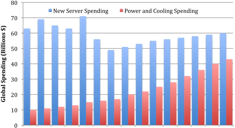
Figure 2.1 – Global Spending for Datacenters
Power reduction can be achieved at various levels of the power supply chain. In this dissertation, we focus on reducing power consumption at the server component level, specifically, at the main memory level. More than 50% of the power consumed by a server is consumed in the central processing units (CPU) and its main memory. Figure 2.2 gives a breakdown of server power from its various components [6].
Figure 2.2 – Power Consumption Breakdown of a Server 0
10 20 30 40 50 60 70 80
1996 1997 1998 1999 2000 2001 2002 2003 2004 2005 2006 2007 2008 2009 2010
G lo b al S p en d in
g
(B
il
li
on
s
$)
New Server Spending Power and Cooling Spending
Power vs. Performance
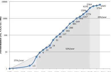
CPU power consumption was trending up with performance gains over the past few decades. It was only when the power wall was reached that designers began to look critically at power consumption. When the cost of cooling a microprocessor became impractical for commodity processors, designers began to reduce performance gains. Figure 2.3 shows how microprocessor performance scaled at roughly 52% per year from 1986 to 2002[7]. In 2002 performance scaling reduced to roughly 20% per year. The reduction of performance gains can be attributed directly to power consumption.
Figure 2.3 – Growth in Processor Performance
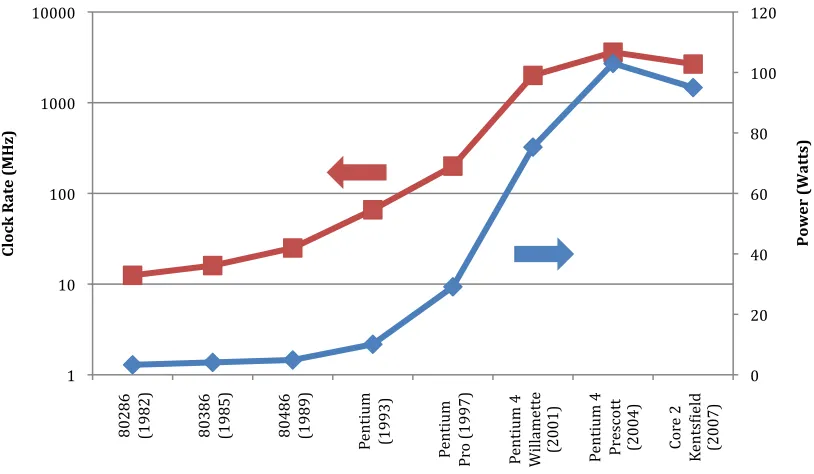
In 2004, Intel released the Prescott microprocessor that was a single core processor using a clock frequency of 3.6 GHz. At the time, processor performance was directly related to clock frequency. Processor manufacturers kept increasing their clock frequency to increase performance. This required the use of a larger amount of
1
1.5 5
9 13 18 24
51 80 117
183 280
481 649 993 1267
1779 2584
4195 5364
5764 6505
1 10 100 1000 10000
1978 1980 1982 1984 1986 1988 1990 1992 1994 1996 1998 2000 2002 2004 2006 2008
P er for man ce (vs . V A X -1 1/ 780)
25%/year
52%/year
transistors. The dynamic power consumed by the transistors can be derived from the following formula.
€
P =CV2f
CLK
The above equation is used to determine the power consumed when charging a capacitor at a frequency of fCLK. The equation states that the dynamic power (P) consumed when charging a capacitor (C) is equal to the capacitance value times the voltage (V) times the frequency.
Before the Prescott microprocessor, voltage scaling was used to successfully contain power consumption to an acceptable value. Voltage scaling, in this dissertation, refers to the process of reducing the external voltage supply at each process shrink (reducing the power by reducing V in the equation above).
Voltage scaling allowed performance to continue increasing while not impacting power consumption by a substantial amount. The limit of voltage scaling was reached when the voltage could not be reduced enough to compensate for the increase in clock frequency. As microprocessors began consuming 100 watts of power or more, the clock frequency started to decrease as seen in Figure 2.4 [7]. This sparked the
Figure 2.4 – Clock Rate and Power for Eight Generations of Intel x86 Processors
Dynamic Random Access Memory (DRAM) Power Consumption
DRAM is currently demonstrating the same type of power limitations as
previously seen in processors. Like processors, voltage scaling in DRAM has masked the issue of a power limit. Unlike microprocessors, market segmentation also plays a major role in masking the power limit. For these reasons, power consumption has taken the back seat to other performance metrics (bandwidth and capacity).
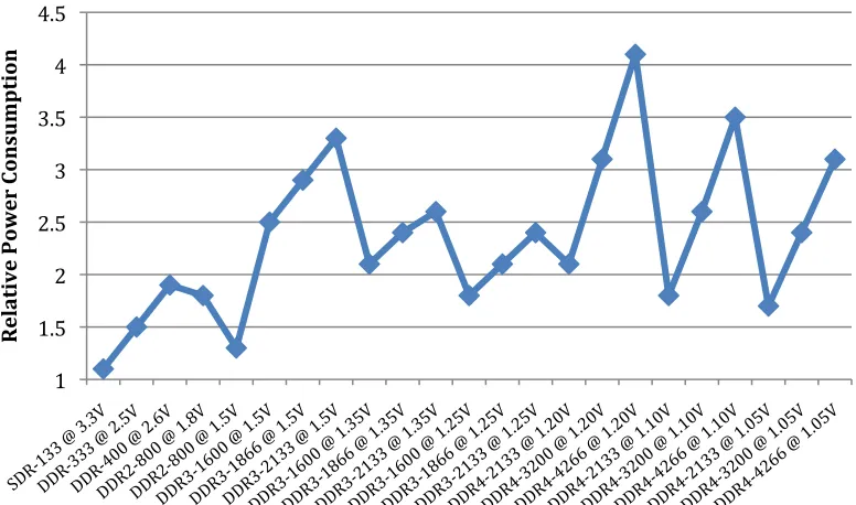
Initial DRAM products used a power supply of 15 volts (1970’s) [8], while current generations are using 1.5 volts [9]. DRAM, manufactured using complimentary metal oxide semiconductors (CMOS), cannot scale their external voltage much further down than 1.0 V. As current consumption continues to rise at each subsequent generation of DRAM, we can visualize the existence of a DRAM power limit. Figure 2.5 shows how DRAM manufacturers are touting voltage scaling as a power reduction metric while not mentioning the practical voltage-scaling limit [10].
0 20 40 60 80 100 120
1 10 100 1000 10000
80286
(1982) 80386
(1985) 80486
(1989)
Pe
nt
iu
m
(1993)
Pe
nt
iu
m
Pr
o (1997)
Pe
nt
iu
m
4
W
ill
ame
tt
e
(2001) Pent
iu
m
4
Pr
escot
t
(2004) Cor
e
2
Ke nt sI ie ld
(2007)
P ow er ( W at ts) Cl oc k R at
e
(M
H
z)
Figure 2.5 – Power Consumption Versus Maximum Frequency in DRAM
Market diversification has led to three major markets for DRAM products:
mobile, desktop, and servers. Currently, mobile memory is designed with power in mind. It consumes less power than desktop memory, but suffers additional cost premiums and performance reductions to achieve the reduction in power. Server memory does not have memory designed specifically for that market segment. Instead, enterprise applications use desktop DRAM. The low component count of desktop DRAM (relative to enterprise) is designed with power as a secondary metric. This causes server applications to be outfitted with inefficient DRAM products; this contributes to the datacenter’s energy efficiency problem.
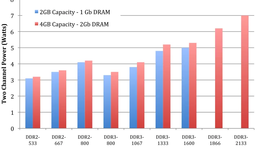
Power consumption of DRAM will continue to increase at a rate greater than that of microprocessors. Figure 2.6 shows the increase in power as a function of both
bandwidth and capacity [6]. The results are misleading, in that, it shows bandwidth
1 1.5 2 2.5 3 3.5 4 4.5
R
el
at
iv
e
having a greater impact than capacity on power consumption. The reason the figure is misleading is that it only analyzes the differences in 2 GB and 4 GB memory modules. Current server architectures can utilize over 300 GB of DRAM [11].
Figure 2.6 – Power Consumption of DRAM Versus Capacity and Bandwidth
A server configuration that uses large amounts of DRAM has a significant impact on power consumption. Servers utilize 16, 32, and up to 64 dual inline memory modules (DIMM) to achieve the required main memory capacity. Depending on its usage, each DIMM can consume up to 20 W of power. An extreme case of power consumption is achieved when 64 DIMMs are used. This could result in an average power consumption of 640 W (10 W per module) and a peak consumption of 1.28 kW (20 W per module). Reducing the power consumption of main memory is left up to server and CPU architects. Servers use complicated usage schemes to reduce the power consumed by main memory.
0 1 2 3 4 5 6 7 8
DDR2-‐ 533
DDR2-‐ 667
DDR2-‐ 800
DDR3-‐ 800
DDR3-‐ 1067
DDR3-‐ 1333
DDR3-‐ 1600
DDR3-‐ 1866
DDR3-‐ 2133
T
w
o
Ch an n el P ow er ( W at ts)
Capacity vs. Power
Table 2.1 shows the effects of both bandwidth and capacity for server configurations utilizing 64 GB of DRAM [6]. Depending on the configuration of the DRAM, which provides 64 GB of memory, the DRAM will have power approaching that of the microprocessor.
Table 2.1 – Power Consumption of Various 64 GB DIMM Configurations
Sample
Card (MHz) Freq Configuration DIMM Tech/Capacity DIMM Power/DIMM (Watts)
64GB System Power (Watts) Card A 1066 Quad Rank x4 2Gb/8GB 15.5 124 Card B 1333 Quad Rank x8 2Gb/8GB 10.6 84.8 Card C 1333 Dual Rank x4 1Gb/4GB 10.6 169.6 Card D 1333 Quad Rank x4 2Gb/16GB 20.5 82 Card E 1600 Quad Rank x8 2Gb/8GB 10.1 80.8 Card F 1600 Quad Rank x4 2Gb/8GB 19.1 152.8
Figure 2.7 – Memory Capacity Impacts System Performance
Current computers are balanced with respect to performance, power, capacity, and cost. Blindly increasing capacity without ensuring that the other factors are considered will cause the innovation to not be applicable to mainstream markets. Instead, new technology that does not maintain system balance will only find its place in low volume and high premium markets.
Table 2.1 and Figure 2.7 show that increasing memory capacity in a server also increases system performance and system power consumption. This causes some servers to not utilize all of the memory slots available due to power consumption.
Bandwidth vs. Power
Another effect of increasing server main memory is that the memory bandwidth begins to degrade as you occupy more memory slots. Figure 2.8 shows that the bandwidth of the memory channel is inversely proportional to the number of occupied memory slots [13].
0 2000 4000 6000 8000 10000 12000 14000 16000
100 150 200 250 300 350 400 450 500
T ra n sa ct io n
s
P er M in u te
Active Users
Figure 2.8 – Devices per Channel Versus Bandwidth
An advanced memory buffer (AMB) is added to the memory module or the motherboard to obviate the bandwidth limitation. The AMB can be thought of as a high-speed serial link between the memory and the microprocessor. Current AMB chips consume the same amount of power as one memory module [14]. For this reason, the AMB was removed from the memory module and placed onto the motherboard. This resulted in one AMB per memory channel. The buffer on board (BoB) configuration is becoming the mainstream approach to solving the capacity issue. Another option of increasing the memory capacity, without degrading bandwidth of the memory channel, is to populate the module with a large number of components. This increases the cost of the memory module.
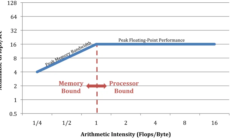
Bandwidth of a processor’s main memory has an impact on its performance. Analyzing the roofline model of Figure 2.9 shows this effect [7]. The roofline model was developed to allow CPU architects a quick and easy way to determine what was limiting a computer’s performance. It uses benchmark data to plot both the peak memory
bandwidth and the peak floating-point operations. The roofline model shows that memory
DIMM
bandwidth limits computer performance by creating stalls, i.e., making the processor wait for its memory. Once memory bandwidth increases to a point that completely satisfies the memory bandwidth criteria for a processor, the processor becomes the bottleneck. In this way, we can show why memory bandwidth improves system level performance.
Figure 2.9 – Roofline Model
The peak memory bandwidth shown in Figure 2.9 is defined as the maximum transfer rate to/from main memory and the microprocessor. This value can be obtained through memory specifications or from benchmarks, such as the steam memory
benchmark. Peak point performance describes the maximum number of floating-point operations that can be completed in a second and varies for different processors. Arithmetic intensity is a term used to describe the number of floating-point operations in a program to the number of data bytes access by a program from main memory [7].
The memory hierarchy uses on-chip cache to supply the required bandwidth to the processing core. The main memory (DRAM) is housed off-chip and has a lower
0.5 1 2 4 8 16 32 64 128
1/4 1/2 1 2 4 8 16
A tt ai n ab le G Fl op s/ se
c
Arithmetic Intensity (Flops/Byte)
Memory Bound
Processor Bound
bandwidth compared to on-chip cache. This is because the main memory is bandwidth limited by the memory channel. The transmission lines of the memory channel have a multi-drop architecture that creates impedance discontinuities.
Each impedance discontinuity causes a reflection into the memory channel. These reflections will degrade the transmitted signal to a point where the receivers on the memory controller, or the DRAM chip, cannot recognize the transmitted or received symbol. This is another reason why the memory hierarchy has been split between on-chip cache and local off-chip main memory.
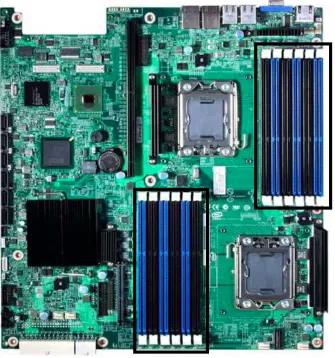
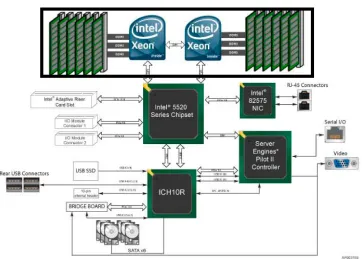
Server Architecture
Figure 2.10 – Intel® Server Board S5520UR
Figure 2.11 – Intel® Server Board S5520UR Functional Block Diagram
Each memory channel consists of 144 signals for a total of 432 signals routed between each processor and its main memory. Creative routing is required to route the three memory channels between the processor and its main memory. Modern
motherboards are approaching 20-layer printed circuit boards (PCB) to achieve this complex routing. The distance between the processor and the main memory is large enough to require the creation of transmission lines. As discussed previously, the multi-drop configuration used in the memory channel limits the sustainable bandwidth in the memory channel.
current memory channel architecture is only sustained by increasing the power consumption and cost of computer systems.
Registered DIMM (RDIMM) Architecture
The third generation of Double Data Rate (DDR3) DRAM is transitioning to become the mainstream memory that is used in server computers. The addition of a register is
required to reduce the load on address and command signals being sent from the memory controller. Servers also require the existence of an additional parity option to ensure error-correcting capabilities for the module. Standard DDR3 modules come in a variety of configurations (capacity, bandwidth, and component count). Figure 2.12 shows the outline of a high capacity DDR3 RDIMM [9].
Figure 2.12 – Typical High Capacity Memory Module
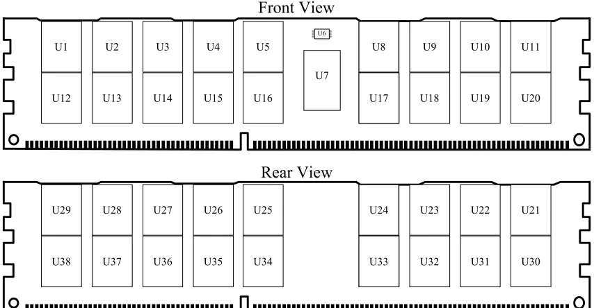
When devices are planar, the maximum number of components that can fit on a module is 36. The memory modules are required to have greater than ten layers on the PCB design to achieve the high capacity memory module; this increases the cost to
U1 U12 U2 U13 U3 U14 U4 U15 U5 U16 U2 U2
U17 U18 U19 U20 U7
U6
U8 U9 U10 U11 Front View U29 U38 U28 U37 U27 U36 U26 U35 U25 U34 U2 U2
manufacture the module. Reaching 72 components per module requires the use of multiple memory die per component. This type of configuration would use dual die (for 72 components) or quad die (for 144 components) memory components.
High-capacity memory modules require the use of memory ranks. A memory rank describes the use of treating a set of DRAM components as one physical bank. Using ranks adds additional termination power to the memory module. As one rank is being read or written to, the other rank must be in a termination state. The module could be treated as one entire rank, allowing for a reduction in power compared to a multi-rank memory module. Depending on the manufacturer and the mode of operation, DDR3 memory modules containing 36 components can consume 1 watt (W) while powered down and 20 W while in active mode. This power consumption adds a limit to the number of memory modules that can occupy a server. Reaching 64 GB of main memory places a severe power constraint on servers.
Memory capacity increases in server platforms results in an increase in costs and power consumption, as previously explained. The termination resistors are responsible for a large portion of the power consumed by the main memory. The termination resistors are included in the DRAM die and are termed on-die termination. A typical termination resistance of the memory module is 60 Ω. The power consumed by the termination
period of 625 ps, and a burst length of eight. The resulting energy consumed by the termination devices, for a read or write, is 216 nano-joules (nJ).
The power consumed by the main memory of a server is reaching a point where DRAM power consumption will be greater than the power consumed by the processors. This will make the main memory the largest consumer of power of the server, and thus the datacenter.
DRAM Architecture
DRAM manufacturers have prioritized memory cell size reduction over all other metrics over the years. This leads to the cost per bit reduction of 9% per year [16]. Manufacturers are forced to place 9% more memory bits into a fixed area to remain profitable. Due to this, the devices and wires used to access the memory cells are also being shrunk at each new process technology. This causes the resistance of both the bitlines and the wordlines of the memory cell to increase. DRAM manufacturers focus on the processing aspect of creating the tiny memory cells rather than increasing the
bandwidth of the memory devices.
The cost of manufacturing DRAM is also a major concern due to the
standardization of main memory. Multiple manufacturers create identical products, which results in a very competitive market space. Die size and process complexity (number of processing steps) are minimized so that costs can remain low. The main memory market is cyclical with deep troughs and high peaks. During the troughs, the costs must be low enough that the manufacturer can remain financially viable, or they go out of business.
8,192 bit page size to reduce the area required for row circuitry. When a read, write, or refresh occurs, the entire page is required to be latched into the bitline sense amplifiers. The bitlines are driven to full logic levels by the bitline sense amplifier. Assuming the maximum activation rate is 100 ns, the bitline capacitance is 200 fF and the page size is 8,192 bits; the sense amplifiers consume ~ 20 mW of power per DRAM die. With 36 components per module, and assuming 16 modules, the power consumed by the bitline sense amplifiers is 11.5 W. This number is directly proportional to the size of the page. If a page is reduced by ½, then the power consumed by the bitline sense amplifiers can also be reduced.
Originally, the page size being large was a benefit to processor designers because of spatial and temporal locality. An accessed page remained open, which negated the row access time when subsequent accesses were to the open page. The introduction of multi-core and multi-thread processors have made temporal and spatial locality less relevant. Independent threads running on a processor have no correlation between their memory addresses. Memory controllers are required to become more complicated so that the requests to main memory can be staggered to preserve temporal and spatial locality. As the number of independent threads increases with more cores and more threads per core, the complexity of memory scheduling will increase.
Problem Statement
CHAPTER THREE – NANO-MODULE
In this chapter, we turn to low cost packaging technologies to propose the creation of an 8-die package and a 32-die memory module. These new form factors are designed for high capacity systems, such as server computers. The technology can be leveraged for use in mobile platforms. The previous chapter described current and past solutions used to maximize memory capacity in server applications. These included the use of a quad-die package and a very low profile DIMM (VLDIMM). The use of advanced packaging, borrowed from multi-chip module (MCM) developers, allows for the creation of three- dimensional integrated circuit (3DIC) configurations.
DRAM memory modules are limited to 36 component slots (18 per side) due to planar size limitations of the module. Dual and quad die components are used to increase the capacity further. If quad die packages are used for all 36 components, then the total number of memory die that can occupy one module is 144 die. This places a capacity limit because only one module can occupy a high bandwidth memory channel.
Brief History of 3DIC
Figure 3.1 – Ultra Dense MCM
The stacked memories are tested and created by first placing the bare die into a recess in a ceramic substrate. After placement, the top of the memory and the ceramic are nearly coincident. A thin film of aluminum is screen printed onto the top of the ceramic to serve as a bonding site for wire bonds. An automatic bonding step is used to wire bond the bare die to the ceramic substrate. The authors show that the bare die can then be electrically tested and/or burned-in.
After testing, both the ceramic component and die component are stacked using identical structures. Insulating glue is used between each layer in the stack. A trimming step is used to trim the ceramic structure away from the bare die. This step leaves the wire bonds exposed on all sides of the cube. This technique is not applicable to modern device sizes. At Boise State, we experimented with thin and thick film deposition and found that the required feature sizes were too small for these types of films.
Val and Lemoine describe a metallic plating step that is used to place metal on each side of the cube. A laser is used to create interconnects by removing excess metal on the sides of the cube. This step provides electrical connection of the entire memory cube. The lateral wiring can be made to form bonding sites. This will allow the cube to be placed onto a MCM that has receiving metal sites available.
ASICS Stacked Memories
Kovar Lid
Kovar Ring Lead Frame
Substrate Al2O3
Several years after this initial memory cube technology was introduced,
researchers described multiple variants of this technology. Irvine Sensors was active in this area and contributed many innovations. In 1993, researchers from Irvine Sensors used IBM interconnect technology to create a 20-DRAM chip memory cube [2]. This new innovation did not require the use of a wire bond step, trimming step, or lateral metal deposition step. Instead, they used a thin film metallic layer to route the memory die’s I/O to the edge of the chips.
A tab of metal was created at the edge of the memory die for each I/O. The tab was used to create a conduction path when all 20 die were glued in a memory cube. A substrate was developed that contained landing sites for the cubes exposed metal tabs. The memory cube was simply placed on the substrate, which contained routing from the landing sites to wire bond sites at the edge of the substrate. Figure 2 shows the resulting 3D memory cube.
Figure 3.2 – Fabrication Steps of the Irvine Sensor Memory Cube
Route pads to edge
Glue chips together with tabs exposed
Connect tabs together
The substantial gains in memory capacity, due to advances in processing technology in the early 90s, made the requirement for 3DIC integration less important than other areas of research, and its interest wavered. Planar spatial limitations are arising again, and the use of 3DIC configurations are once again being explored. Samsung engineers were the first to demonstrate a 3DIC stack of DRAM die that utilize through silicon via (TSV) technology [3].
Through Silicon Via
TSV interconnects are being pursued by a large number of private and public
organizations. Industry wide financial investment into TSV integration increases the chances that the technology will become the main stream for 3DIC.
Samsung engineers reported on stacking four 2 Gb DDR3 DRAM die using TSV technology. 300 TSV were used for both signals and power routing between the four chips. They realized that the use of four identical chips was not necessary. Clock recovery, data path, and I/O circuits were only required on the die that had the physical connection to the substrate. This allowed for lower power consumption and increased die efficiency for the three other chips that did not house the redundant circuits. They used the additional savings to place redundant TSV structures; this increases the yield of the entire 3DIC. Figure 3.3 shows the block diagram of the 8 Gb 3DIC [3].
Figure 3.3 – Conceptual View of the 3DIC
PCB Primary Chip Secondary Chips TSV (~300) Rank 0 Rank 1 Rank 2 Rank 3 DRAM Core DRAM Core DRAM Core DRAM Core
TSV technology is suitable for 3DIC because they have a low resistance (< 10 Ω)
and take up little silicon area (10 µm2). However, the technology is limited due to cost and integration challenges. A consortium of industry companies are working together to develop low cost TSV technologies. In 2009, two technologies were selected as front-runners in developing a low cost TSV technology. An aggressive goal for cost of ownership was determined to be $150 per wafer [4]. The price reflects the economic sustainability of TSV technologies in modern wafer processing. Substrate noise injection, reliability concerns, and height restrictions are some of the technical issues facing TSV integration. These reasons make TSV technology a good avenue to pursue, but their integration is costly and uncertain as to when the technology will become mainstream.
The 3DIC using TSV solution that Samsung developed shows how this approach can lead to lower power and higher capacity than traditional quad die packages [3]. There are two issues with this approach: one being cost and the other being the creation of a new memory product. Memory manufacturers typically have one (or two) product offering(s) in a particular product line (DDR3) and density at a time. The Samsung approach would require the creation of an additional two offerings of a particular product line. The two additional offerings would be the bottom device in the memory stack and the three top die in the memory stack. Each of these devices would require a substantial amount of sales to offset the initial investment.
Figure 3.4 – Typical NAND Stacking Technique
The memory devices are stacked in a staggered fashion. Each additional memory die is offset from the previous memory die in the stack. This allows a wire bond to attach to each die’s exposed input/output wire bond pad. The wire bond approach allows for a low cost memory solution, but also reduces the bandwidth. The shared wire bond
connection adds a large capacitance and inductance to the input/output pad. The parasitic nature of the wire bond creates a bandwidth limit to the input or output signals being driven to/from the memory die. This dissertation proposes a low cost stacking approach that removes the need for the shared wire bond connection, thus increasing the available bandwidth.
Alternative methods have been proposed to increase the bandwidth and
Figure 3.5 – A High Cost Premium 3DIC Configuration
Black et al. thoroughly discuss the benefits of creating a 3DIC configuration that contains a microprocessor along with memory die in the aforementioned reference. Increased bandwidth and lower power are touted as key figures of merit, but cost is not considered. The inclusion of multiple advanced packaging techniques (C4 bumps,
through silicon vias, die to die vias, and a nascent heat sink technology) increases the cost to produce this type of 3DIC. This dissertation proposes a stacking technique that uses heavily verified technologies to achieve the same types of bandwidth and power metrics with out substantially impacting cost.
Low Cost Stacking Approach
Figure 3.6 – Stepped Device Stacking
The invention describes a variety of ways to connect the angled die to the substrate. The die can be attached with a wire bond (as depicted in Figure 3.6) or with a solder ball. Alternative inventions described attaching the angled die to the substrate by applying solder to both the substrate and die landing sites, placing the two together so that their solder touches, and reflowing the stack to get electrical connection. Figure 3.7 shows an alternative connection method detailed by engineers at MCNC [19].
Substrate Connection
Figure 3.7 – Alternative Method of Angle Bonding the Die to the Substrate
These stacking techniques allow multiple die to be stacked together in a 3DIC configuration. The major advantages of angled bonding technology are cost, power, and bandwidth. The cost of the high capacity memory stack can be greatly reduced by using low cost packaging techniques. The stacking technology places the memory die into a small area allowing for a reduction in the trace lengths. The trace length reduction also reduces the parasitic load that is driven by the I/O of the memory die. This has a benefit of reducing the power consumed by the memory die. The memory chips are placed very close together and the termination can be shared between the die. A configuration where every fourth memory die’s termination is active can be used and would result in
increase the bandwidth of the memory die due to the reduction in parasitic capacitance, resistance, and inductance.
Nano-Module
Leveraging all of the benefits of this technology requires the use of an active silicon substrate. Placing registers/buffers directly below the memory die allows for the
elimination of the termination resistors on the memory die. Termination is only necessary at the I/O of the substrate.
Redistribution Layer
Figure 3.8 – Redistribution Layer Used to Route Pads to the Edge of the Die
A major concern when routing the power signals to the edge of the die is the voltage drop. The voltage drop is due to the high current that can pass through the power and ground routing. Current DRAM die are getting smaller, which limits the space available to route the signals. RDL layers that are used on silicon die can achieve a minimum of 10 µm of spacing and 10 µm of width for the metal tracks. Using two RDL layers to route the signals is preferable but requires expertise at the RDL processing facility. Non-uniformity on the DRAM substrate makes processing the RDL layers difficult. Currently, DRAM die have a higher number of internal pads than external pads, meaning that some power and ground buses need to be consolidated.
RDL Layer Edge RDL Pads
The DRAM die size places a limit to the number of I/O pads that can be placed on its edge. A typical DRAM die will have an edge width of approximately 8 mm and a typical pitch of soldered connections is 200 µm. This places a limit of 40 I/O pads that can sit on the edge of the DRAM die. If the solder connection pitch is reduced to 133 µm, it is possible to fit 60 I/O pads on the edge of the DRAM die. This is sufficient for DDR2 memory parts, but DDR3 memory die are using 78 external connections to the memory die (mainly due to an increase in the number of power and ground balls).
A solution to this problem is to use a material surrounding the silicon die that acts as a fan out for the RDL routing. This is used in some wafer scale packaging (WSP) or very fine ball grid array (VFBGA) packages. Infineon demonstrated their fan out
technology for their WSP technology [20]. Figure 3.9 shows a cross section view of a die that has been surrounded by a mold compound that creates additional space for I/O routing using RDL layers. The mold compound extends the size of the chip to allow for a large area to place an RDL layer. The bottom of Figure 3.9 contains the solder balls used to pass the signals from the chip to a substrate.
Figure 3.9 – Fan Out Used in Wafer Scale Package
Using RDL layers on the DRAM die allow the signals to be transported from the center of the memory chip to the edge of the memory chip. This solution is applicable for
Mold Compound (Fan-Out)
Chip
a single row of pads on the DRAM or a double pad row DRAM architecture. Once the signals are routed to the edge of the die, it is possible to mount the chips at an angle onto the substrate.
Substrate Design
The substrate design can be either purely passive (redistribution layer(s) only) or active (substrate contains circuitry). Both types of substrates require mounting sites for the connection to the DRAM die and a redistribution network to connect the DRAM die to the edge wire bonding sites. Figure 3.10 shows a mock up of a typical substrate design.
Figure 3.10 – Substrate Mock-Up Showing Wire Bond and Connection Sites
Assuming a 200 µm die to substrate connection pitch and 78 connections on each memory die, it can be shown that the total length of a single landing site in Figure 3.8 is
Wire Bond Sites
15.5 mm (15.4 mm plus a connection diameter of 100 µm). This will require the use of a fan out material used on the DRAM die.
Module Size Calculations
The spacing of each wire bond connection row is determined by viewing Figure 3.11.
Figure 3.11 – Geometry Used to Determine Die to Substrate Connection Column Pitch
It is found that the pitch of the wire bond connection column (p) is required to be
€
t sinα, where α is the angle of attachment and t is the thickness of the die and any
adhesion. The height of the unmolded package is determined by viewing Figure 3.12.
Figure 3.12 – Geometry Used to Determine the Height of the Package
α
p
t
ch
d
α
wdie - x
x
ch
tsub α
h1
Using the geometry of Figure 3.12, the height of the package can be determined. This geometric analysis can be taken further to determine the exact dimensions of the unmolded package. The following equations summarize the dimensions of the unmolded package. tcon pictch in the following equations refers to the pitch of the connectors used to connect the die edge pads to the substrate.
€
height=tsub thickness+tconnection+tdie thickness
cosα +
(
tdie width −tdie pad to edge)
sinα€
width=
(
no.signals−1)
tcon pitch+tcon diameter+2(
tdie to pad edge+twb1 +twb2)
€
length=2
(
twb1+twb2)
+sinα⋅tdie thickness+#die−1
(
)
tdie thicknesssinα +cosα⋅tdie width
The formulas above use twb1 to represent the spacing between the center of the pad on the memory die and the silicon die, and twb2 as the distance from the center of the pad on the memory die to the edge of the substrate. We can use these equations to determine the size of several configurations. We will assume the following parameters going
forward: tsub = 500 µm, tdie = 200 µm, attach angle = 20º, dconnection = 100 µm, pad to edge spacing of 200 µm, and die size of 8 mm x 10 mm. Using these parameters, a 32-die package would be 3.48 mm by 16.7 mm by 26.5 mm, and an 8-die package would measure 3.48 mm by 16.7 mm by 12.5 mm.
include passive components (capacitors and inductors) to be created with the top levels of metal. It is even possible to transfer some of the functionality of the memory controller onto the substrate. Once the substrate is defined, it is possible to mount the memory stack on the substrate as seen in the cross section in Figure 3.13.
Figure 3.13 – Cross Section View of the Memory Stack
The memory stack can be connected to the microprocessor in varying ways. It is possible to place the memory stack into the same package as the CPU allowing for an extreme reduction in the memory channel power and an increase in the bandwidth of the main memory. Novel interconnect technologies can be used to connect the substrate to the microprocessor. An example of a novel interconnect is a wireless capacitive-coupled interconnect that allows for an order of magnitude increase in the density of interconnects between two die.
It is possible to configure the memory stack as a stand-alone memory module that is placed in an assembly package, much like the microprocessor. This module can be placed in a socket on the motherboard or permanently attached to the motherboard. Depending on the replacement policy, it might be better to use the socket approach. The socket approach allows for the possibility of replacing a defective module, upgrading existing modules, or allowing for scalability of the motherboard’s memory.
memory die. This is true if the stack is placed within an MCM with the processor or as a stand-alone module. A complete thermal solution is outside of the scope of this
dissertation but the following discussion is provided for completeness. Thermal Options
Standard techniques used to remove heat off of the memory module are not applicable to the proposed nano-module due to the novel stacking technique. Figure 2.12 shows that standard DRAM modules place the memory die in a planar manner. This allows for the use of a heat spreader to be placed over the memory module. Thermal paste is placed on the molded die allowing for a high thermal conductivity path between the mold
compound and the heat spreader. Heat passes through the thermal paste and collects on the heat spreader. Typically, air is passed over the memory modules allowing the heat to be removed from the system. Without the heat spreader, the nano-module requires heat to be removed from the top or bottom of the module as seen in Figure 3.14.
Figure 3.14 – Heat Transfer of the Nano-Module
When power is consumed on the memory die, heat is produced. The heat generated from a die follows the path of the greatest thermal conductivity. The thermal conductivity of materials is described in units of Watts per meter Kelvin (W/mK) and specifies the material’s ability to conduct and transfer heat. Silicon and metal have a
Mold Compound
thermal conductivity greater than 100 W/mK, while the mold compound can have a thermal conductivity less than one W/mK.
The heat generated on a memory die will pass through adjacent memory die, wire connections at the bottom of the die, silicon substrate, and mold compound. The rate of heat transfer is lowest at the mold compound. This is due to the difference in the thermal conductivity between the materials. If air is passed over the top and bottom of the
module, some of the heat will be removed. The large path through the silicon die to the wired connections at the bottom of the die will lead to a large temperature gradient.
The temperature gradient will result in a wide variety of performance across the memory die and creates hot spots. The temperature gradient causes a performance loss. The hot spots can degrade the life of the memory die due to high temperature stresses. Heat must be transferred from the memory die to the outside of the package in order to prevent these affects. Figure 3.15 shows a solution for heat removal on the nano-module.
Figure 3.15 – Proposed Heat Removal Solution
Figure 3.15 shows the use of a high thermally conductive material placed between the memory die and extending to the top of the nano-module. A heat removal plate, with high thermal conductivity, is placed at the top of the nano-module. The heat removal plate is used to transfer the heat out of the nano-module. Once the heat is transferred to
Heat Removal Plate
the heat removal plate, a variety of techniques can be used to remove the heat. These include passive and active heat sinks.
CHAPTER FOUR – DRAM ARCHITECTURE
Increasing the bandwidth of the main memory can be accomplished by increasing the number of data signals used by the memory chip. Increasing the number of data signals using conventional interconnect technologies increases power consumption. Wireless interconnects are being used in 3DIC configurations due to their low power and high bandwidth configurations. Leveraging these advantages in DRAM requires several changes to the memory chip. This chapter develops a DRAM architecture that is created for low power and high bandwidth applications. The architecture is well suited for wireless interconnect technologies.
4 Gb DRAM Architecture
Figure 4.1 – A 4 Gb DRAM Architecture
Capacitive-coupled interconnects work when two die are placed face to face and a capacitor is formed between the top level of metal on each die. This approach works well when the I/O pads are placed on the edge of the chips. The first step in developing the new DRAM architecture was to move the pads to the edge of the die. The second step was to change the structure of the memory banks and periphery circuitry to maximize array efficiency while keeping column and row cycle times constant. Making these changes resulted in the discovery of several challenges.
Edge Aligned I/O Pads
Moving the pads to the edge would require address, command, and data signals to be buffered into the memory array. The time difference experienced from routing the data
7.0 mm
10.2 m
m
Chip Size = 71.4 mm
2Array Efficiency = 57.7%
signals to the closest and furthest memory arrays would create a significant design challenge and increase the cycle time specifications of the memory. The addition of buffers would also increase the power consumption of the memory die. Due to these challenges, an alternative solution was needed.
A centralized row and column structure can be used to reduce the die size. The centralized column structure requires signals to be driven 5 mm to the edge of the
memory array. Comparing this to the previous column path, which drove data signals 2.5 mm, it is apparent that the column path frequency will decrease. However, the use of a wide I/O interface will allow for more bits to be read in parallel. This, in effect, can normalize the column throughput. With this approach, column path throughput can be normalized, or increased, at the expense of access latency. The centralized row structure follows the same logic as the centralized column structure.
Main memory used for desktop and server applications operate with eight internal banks. This allows a single row to be active in each bank simultaneously, allowing the row cycle time to be circumvented. The eight-bank architecture allows for access scheduling to open word lines in each bank. Due to this, the row cycle is much greater than the column cycle time. The row cycle time is dominated by the time it takes to drive the large parasitic resistance and capacitance of the word line. This allows the typical access time to be a function of the column cycle time and not the word line cycle time. The large row cycle time and access scheduling allows for the design of a central row structure to service the memory banks.
Figure 4.2 shows the representation of eight internal banks in the DRAM
memory core operation frequency by reducing the local I/O metal parasitic resistance and capacitance.
Figure 4.2 – DRAM Architecture with Edge I/O
The implemented architecture decisions allowed for the integration of a
capacitive-coupled interconnect residing at the edge of the memory chip. Changing to a centralized column and row circuitry allowed for an 8.0% decrease in chip size and an 8.8% increase in array efficiency. The die size savings can be used for an increase in the number of die per wafer (cost), or additional support circuitry can be added to the die while keeping the die size constant. Establishing the centralized structures early in the architecture definition allowed for enough research and development time to implement the architecture.
6.7 mm
9.8 m
m
Chip Size = 65.66 mm
2Array Efficiency = 62.79%
Edge I/O Interface
The initial wide I/O architecture allowed for an immediate sense of the challenges associated with integrating capacitive-coupled interconnects on a DRAM chip. The initial choices were made with respect to chip size and array efficiency, while the challenges were in trying to buffer the signals into the DRAM chip. Alleviating some of the initial challenges required the communication channel be placed on the side of the DRAM chip rather than the bottom. Placing the communication channel on the side of the DRAM chip requires an additional review of the 512 Mb bank structure.
Bank Structure
When a word line is activated in a memory bank, a page of data is latched into the bit line sense amplifier. The number of bit line sense amplifiers activated is referred to as a page. Current DRAM devices utilize an 8k page. The power needed to charge 8k bit line capacitance sets the majority of the power consumption of the DRAM chip. While 8k bit line memory bits are read during a single access, only 64 bits are sent off-chip, which leads to a very low energy efficiency per bit accessed. A wide I/O architecture will increase the number of bits that can be driven off of the chip, greatly increasing the energy efficiency of DRAM products. The page size of the DRAM can also be reduced because the temporal and spatial locality is decreasing as we move towards multi-core/multi-thread applications.
memory access scheduler and multiple banks has allowed this technology to continue scaling.
The memory access scheduler is used to store outstanding data requests to and from main memory. The requests are staggered in a way to ensure temporal and spatial locality. As the number of independent threads increases, the hardware required to sustain proper temporal and spatial locality to an open row will begin to have diminishing
returns. The 8k-page size is becoming irrelevant and a reduction in the page size is a logical next step. Reducing the page size has a significant impact on the memory power consumption and the hardware required to reduce the page size by two is minimal. The bank structure used in the modified 4 Gb DRAM architecture realizes the same 8k page size, with the realization that a reduction in page size requires minimal effort.