Optimised ASIC Ready FPGA Design
Prof Sandip Nemade, Mr Mohd AhmedAbstract— FPGA devices are an important component in many modern devices. This means that it is important that VLSI designers have a thorough knowledge of how to optimize designs for FPGAs. While the design flows for ASICs and FPGAs are similar, there are many differences as well due to the limitations inherent in FPGA devices. To be able to use an FPGA efficiently it is important to be aware of both the strengths and weaknesses of FPGAs. If an FPGA design should be ported to an ASIC at a later stage it is also important to take this into account early in the design cycle so that the ASIC port will be efficient.
This paper investigates as how to optimize a design for an FPGA and what steps should be taken in the design to enable seamless porting from FPGA to ASICS for volume production
Keywords—Optimised FPGA vs ASICS, FPGA to ASIC Porting.
I. INTRODUCTION
FPGA designs enjoy a lot of success; however, most of the FPGA design starts are likely to be for fairly low volume products as the unit price of FPGAs make them unattractive for high volume production. Similarly, most of the ASIC design starts are probably only intended for high volume products due to the high setup cost and low unit cost of ASICs. Even so, the ASIC designs are likely to be prototyped in FPGAs. And if a low volume FPGA product is successful it may have to be converted to an ASIC If the FPGA design was not designed with an ASIC in mind from the beginning, it may be hard to create such a port. This paper will classify and investigate various FPGA optimizations to determine whether they make sense to use in a product that may have to be ported to an ASIC and will try to compare as a whole ASIC design with an FPGA design based on performance
II. MODERN FPGA’S
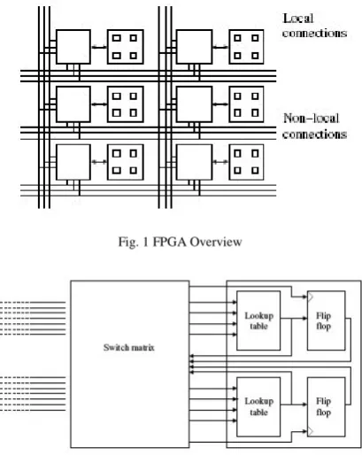
Todays FPGAs are much more complex devices and a number of inbuilt optimizations have been done to improve the performance of important design components. For example, in Xilinx FPGAs, a CLB has been further divided into slices. A slice in most Xilinx devices for example, consists of two LUTs and two flip-flops. There is also special logic in the slice to simplify common operations like combining two LUTs into a larger LUT and creating efficient adders. The basic architecture in Fig 1 and Fig 2 is not very optimal when a memory is needed. To improve the performance of memory dense designs, modern FPGAs have embedded memory blocks capable of operating at high speed. In a Virtex-4 FPGA, an embedded memory, referred to as a block RAM, contains 512 words of 36 bits each. (It is also possible to configure
Fig. 1 FPGA Overview
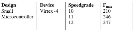
Fig. 1 CLB and Switch matrix
half of the LUTs in the CLBs as a small memory containing 16 bits, this is referred to as a distributed RAM.) In contrast, a Stratix-3 from Altera have embedded memory blocks of different sizes. There are many blocks that contain 256 36-bit words and a few blocks with 2048 72-bit words.
To improve the performance of arithmetic operations like addition and subtraction, there are special connections available that allows a LUT to function as an efficient full adder. This is referred to as a carry chain. A carry chain is also connected to adjacent slices to allow for larger adders to be created. To improve the performance of multiplication, hard wired multiplier blocks are also available in most FPGAs, sometimes combined with other logic like an accumulator. In a Virtex-4, a block consisting of a multiplier and an
A. XILINX FPGA DESIGN
A typical FPGA design flow consists of the following steps (in more advanced flows some of these steps may be combined):
•Synthesis: Translate RTL code into LUTs, flip-flops, memories, etc.
•Mapping: Map LUTs and flip-flops into slices
•Place and route: First decide where all slices, memory blocks, etc should be placed in the FPGA and then route all signals that connects these components
•Bitfile generation: Convert the netlist produced by the place and route step into a bitstream that can be used to configure the FPGA[9]
•FPGA Configuration: Download the bitstream into the FPGA
There are also other steps that are optional but can be used in some cases. A static timing analyzer, for example, can be used to determine the critical path of a certain design. It can also be used to make sure that a design is meeting the timing constraints, but this is seldom necessary as the place and route tool will usually print a warning if the timing constraints are not met.
There are special tools available to inspect and modify the design. A floorplanning tool[10][11] allows a designer to investigate the placement of all components in a design and change the placement if necessary. An FPGA editing tool can be used to view and edit the exact configuration of a CLB and other components in terms of logic equations for LUTs, flip-flop configuration, etc. It will also show how signals are routed in the FPGA and can also change the routing if necessary.
III. OPTIMIZING DESIGN FOR FPGA’S
Optimizing an algorithm to an FPGA will use the same general ideas as optimizing for ASICs. The basic idea is to use as much parallelization as required to achieve the required performance.
A. High level optimization
Adding pipeline-stages, if possible, is a simple way to increase the performance in both FPGAs and ASICs. It is usually especially area efficient in FPGAs, since most FPGA designs are not flip-flop limited, which means that there are a lot of flip-flops available and an unused flip-flop is a wasted flip-flop. Although a general technique, some designs cannot easily tolerate extra pipeline stages (e.g. microprocessors) and other methods are required in those cases.
All ASIC methodologies, structured or standard cell, require complete and accurate design constraints to control logic placement. Also, since direct netlist conversion is no longer common due to the inherent performance limitations for large designs, proper constraints are required also for synthesis. A fully constrained design requires all of the device logic to be fully synchronous, meaning that there cannot be
asynchronous paths inside the design (e.g. ring oscillators), although multi-cycle paths are fine.[1]
Constraining a design properly is made more difficult for designs with:
1) Large numbers of clock domains, such as seen when SerDes are used
2) Designs with source synchronous interfaces, such as DDR or DDR2
3) Designs that use multiple functional modes, where different clocks might be present on the same clock tree
Also, tools like Synplicity’s Synplify, the effective standard for large FPGA synthesis, allow the user to set a default frequency for all otherwise unconstrained paths. Therefore, a partially constrained design will create, without any error flags, a complete and working design in the lab. However, those same constraints would not be sufficient for an ASIC. To work around this, customers needed to actively check for unconstrained design paths in the design.
Another way to improve the performance of an FPGA is by utilizing all capabilities of the embedded memories. In ASICs, dual port memories are more expensive than single port memories. Therefore it makes sense to avoid dual port memories in many situations. However, in FPGAs, the basic memory block primitive is usually dual-ported by default. Therefore it makes sense to use the memories in dual-ported mode if it will simplify an algorithm. Similarly, each memory block in an FPGA has a fixed size. Therefore it can make sense to decrease logic usage at a cost of increased memory usage as long as the memory usage for that part of the design will still fit into a certain block RAM. However FPGAs, at power-up, require some time to load in the input program file and setup the device. FPGA program files also set the initial RAM values for an FPGA. This is contrary to the situation for ASICs where the initial RAM state is unknown and initialization is required after power-up. Therefore, customers looking to port designs from FPGA to ASIC need to design so that they do not rely upon RAM bit settings without first manually initializing those RAM
s.
Another issue is that the FPGA RAMs come in a very few discrete sizes. Customers needing a 4Kb RAM may have to use a much larger 18Kb RAM in the FPGA. That is fine in the FPGA as long as the design fits, but in an ASIC we can trim out the wasted RAM area by making sure that only a 4Kb RAM is instantiated. To do this, the logical RAM wrapper (e.g. 4Kb) should be separated from the physical RAM instantiation (e.g. 18Kb in FPGA and 4Kb in ASIC). By placing the physical memory instances in a file, the designer can maintain one design with two sets of memory files that will work in either technology. By simple replacing the file containing the physical FPGA memory instance definitions with a new file containing the compiled ASIC RAM instance definitions the design can be made ASIC ready.Design Device Speedgrade Fmax
Small
Microcontroller
Virtex -4 10 11 12
210 246 247
other way around as well. Coming up with a way to reduce a multiplier from 16 × 16 bits to a mere 13 × 13 bits at the cost of additional logic is not going to help in terms of resource utilization
B. Low Level logic Optimization
In many cases there is no need to go further than the optimizations mentioned in the previous section. However, if the performance that was reached by the previous optimizations was not satisfactory, it is possible to fine-tune the architecture for a certain FPGA. Some examples of how to do this are:
• Modify the critical path to take advantage of the LUT structure. For example, if an 8-to-1 multiplexer is required it will probably be synthesized, utilizing a total of 4 LUTs distributed over two slices and taking advantage of the built-in MUXF5 and MUXF6 primitives when synthesized to a Virtex-4. However, if it is possible to rearrange the logic so that the inputs to the mux are zero in case the input is not going to be selected, the mux can be rearranged using a combination of or gates and muxes. The design can be fine tuned to make sure that the algorithms are mapped to the FPGA in such a way that adders can be efficiently combined with other components such as muxes while keeping the number of logic levels low.
•In a Virtex-4 some LUTs can be configured as small shift registers. This makes it very efficient to add small delay lines and FIFOs to a design.
• Bit serial arithmetic can be a great way to maximize the throughput of a design by minimizing the logic delays at a cost of increased complexity. To be worthwhile, a large degree of parallelism must be available in the application. Bit (or digit) serial algorithms can also be a very useful way to minimize the area cost of modules that are required in a system but have low performance requirements, such as for example a real time clock.
C. Placement optimizations
If the required performance is not reached through either high or low level logic optimizations it is usually possible to gain a little more performance by floorplanning. There are two kinds of floorplanning available for an FPGA flow. [3],[4]The easiest is to tell the backend tools to place certain modules in certain regions of the FPGA. This is rather coarse grained but can be a good way to ensure that the timing characteristics of the design will not vary too much over multiple place and route runs. The other way is to manually (either in the HDL source code or through the use of a graphical user interface), describe how the FPGA primitives should be placed. For example, if the critical path is long (several levels of LUTs), it makes sense to make sure that all parts of it are closely packed, preferably inside a single CLB due to the fast routing available inside a CLB. If the design consists of a complicated data path, the entire data path could be designed using RLOC attributes to ensure that the data path will always be placed in a good way. The advantage of floorplanning has been investigated in [2][10], and was found to be able to improve the performance from 30% to 50%.Today, the performance
increase that can be gained from floorplanning is closer to 10% or so and it is often enough to floorplan only the critical parts of the design [3].
D. Optimizing for Reconfigurability
The ability to reconfigure an FPGA can be a powerful feature, especially for the FPGA families where parts of the FPGA can be reconfigured dynamically without impacting the operations of other parts of the FPGA. This can be a very powerful ability in a system that has to handle a wide variety of tasks under the assumption that it doesn’t have to handle all kinds of tasks simultaneously. In that case it may be possible to use reconfiguration, similarly to how an operating system for a computer is using virtual memory. That is, swap in hardware accelerators for the current workload and swap out unused logic. This can lead to significant unit cost reductions as a smaller FPGA can be used without any loss of functionality. While this ability is powerful, it is only supported for a few FPGAs and the support from the design tools is rather limited. But the configurability of an FPGA can still be useful, even if it is not possible to reconfigure the FPGA dynamically. One example is to use a special FPGA bitstream for diagnostic testing purposes (e.g. testing the PCB that the FPGA is located on). While such functionality could be included in the main design it may be better from a performance and area perspective to use a dedicated FPGA configuration for this purpose
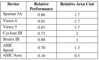
E. Speed Grades, Supply Voltages and Temperature
Due to differences in manufacturing, the actual performance of a certain FPGA family can vary by a significant amount between various specimens. Faster devices are marked with a higher speed grade than slower devices and can be sold at a premium by the FPGA manufacturers. There is no exact definition of what a speed grade means, but in general, going up one speed grade means that the maximum clock frequency will increase around 15% depending on the design and the FPGA [13],[14]. An example of the impact of the speed grade on two designs is shown in Table I. (The unit that is tested is a small microcontroller with a bus interface, serial port and parallel port.)
TABLE I: IMPACT OF SPEEDGRADE
available, we can specify that the FPGA will not exceed a certain temperature.
F. Fmaxfor FPGA Designs
There are many parameters that impact the maximum clock frequency. Perhaps the most important is the synthesis tools and the place and route tools. All tools in the FPGA design flow have many options that will impact the maximum frequency, area, power usage, and sometimes even the correctness of the final design.
1) Timing Constraints
Perhaps the most important of these options are the timing constraints given to the tools. The tools will typically not optimize a design further when it has reached the user specified timing constraints. If the timing constraint cannot be achieved, different tools behave in different ways. Xilinx’
tools will spend a lot of time trying to meet a goal that cannot be achieved. It is also not uncommon that an impossible timing constraint will mean that the resulting circuit will be slower than if a hard but possible timing constraint was specified. Altera’s tools, on the other hand do not seem to be plagued by this particular problem though. If a very hard timing constraint is set, Altera’s place and route tool will give a design with roughly the same Fmax as can be found when sweeping the timing constraint over a wide region. (This behaviour has been tested with ISE 10.1 and Quartus II 8.1. [2],[4]) Another important thing to consider is clock jitter. As clock frequencies increase, jitter is becoming a significant issue that designers need to be aware of. It is possible to specify the jitter of the incoming clock signals in the timing constraints. The use of modules like DCMs and DLLs will also add to the jitter (this jitter value is usually added automatically by the backend tools)[12]. This is important since the jitter will probably account for a significant part of the clock period on a high speed design.
IV. METHOD SUMMARY FOR OPTIMIZATION The method mentioned in this paper to optimize FPGA designs can be summarized as given below.
• Do not fix the design specification until a prototype has shown where the performance problems are located and a reasonable plan on how to deal with the performance problems has been finalized. To reach the highest performance it may be necessary to implement a prototype with much of the functionality required of the final system before the design specification can be finalized. Use synchronous design methods and avoid using techniques such as latches and clock gating
• Investigate if the synthesis tool has used suboptimal constructs. If so, rewrite the HDL code to infer or instantiate better logic.
•Investigate if floorplanning can help the performance as well.
• Vary synthesis and backend options to determine which options lead to the highest performance.
•Manage the timing constraints appropriately for the tool that is used for place and route (e.g. increase the timing constraints
iteratively until it is no longer possible to meet timing when using Xilinx devices)
•Further, the timing constraint settings assume a clock with no jitter and the worst case parameters for temperature and supply voltage
• Be wary of bugs in both the design and the CAD tools. Always check that the reported area and performance are reasonable
V. PERFORMANCE COMPARISON OF LOGIC IMPLEMENTED IN FPGA & ASIC
The performance comparison of logic implemented in an FPGA and an ASIC will be compared looks like a relatively easy task.
Select a design to test
2. Synthesize the design for an FPGA 3. Synthesize the design for an ASIC 4. Compare the performance of these designs
The best way to do this would be to compare an FPGA where the contents of all look-up tables are optimal and the routing is optimal to an ASIC design where the placement, sizing, and routing are all optimal.[1] This is unfortunately an optimization problem of extreme complexity, even for small designs. This part intends to highlight is the impact of various FPGA optimized constructs when the design is ported to an ASIC. Also the relative cost of various design elements in terms of area and frequency are mentioned. The intention is to show whether a certain construct is a good idea to use in a certain FPGA. Another important factor that will be discussed is if it is a good idea to use a certain architecture in an ASIC.
A. Adders
Device Relative Performance
Relative Area Cost
Spartan 3A 2.2 1
Virtex 4 1.9 1
Virtex 5 1.7 1
Cyclone III 2.2 1
Stratix III 2.1 1
ASIC Speed 1.8 0.12
ASIC Area 1.8 0.12
FIG. 3. 32 Bit Adder
FIG. 4. 32 Bit 3 Operand Adder
FIG. 5. 32 Bit 2-1 Mux
TABLE III
32 BIT ADDER PERFORMANCE COMPARISON
Speed
ASIC Area 0.11 0.21
TABLE IIIII
32 BIT 3OPERAND ADDER PERFORMANCE COMPARISON
Device Relative Performance
Relative Area Cost
Spartan 3A 0.86 1.7
Virtex 4 0.81 1.7
Virtex 5 0.83 1.7
Cyclone III 0.73 2
Stratix III 0.88 1
ASIC
Speed 0.70 1.3
ASIC Area 0.10 0.5
B. Multiplexers
A very important part of many datapaths is the multiplexer (mux). An FPGA based solely on 4 input LUTs can implement a 2n-to-1 mux using 2n − 1 LUTs. However, modern FPGAs usually have some sort of hardwired muxes in the slices and CLBs to optimize the implementation of muxes. In this case it is possible to implement a 2n-to-1 mux using only 2n−1 LUTs. In the Virtex-4 architecture, muxes of sizes up to 32-to-1 can be optimized in this way. It is clear that muxes are not likely to be a big problem when porting a design to an ASIC. However, it may be possible to improve the design of the ASIC port by inserting extra muxes in the design. A cheap way to do this could be to replace a mux based bus with a full crossbar. Table IV show the relative performance and area of a 2-to-1multiplexer.
C. Multipliers
The most common method for multiplication in FPGAs today is to use one of the built in multiplier blocks that are present in almost all modern FPGAs. While some FPGAs such as the Virtex-II and Spartan-3 have a standalone multiplier as a separate block[7], other FPGAs also integrate accumulators into the same block. The later are commonly called DSP blocks.[5]
TABLE IVV
32 BIT 2-1 MUX PERFORMANCE COMPARISON
Device Relative Performance
Relative Area Cost
Spartan 3A 1 1
Virtex 4 1 1
Virtex 5 1 1
Cyclone III 1 1
Stratix III 1 1
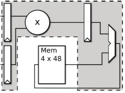
FIG. 6. MAC unit with 4 Accumulator registers mapped to DSP-48
TABLE V
MAC UNIT WITH DSP-48 PERFORMANCE COMPARISON
Device Relative
Performance
Relative Area Cost
Virtex 4 0.45 30
Virtex 5 0.41 35
ASIC Speed 0.2 5.3
ASIC Area 0.079 2.2
In many cases there are optional pipeline stages built into these multipliers and the maximum performance can only be reached if these pipeline stages are utilized.[6] In the Spartan 3A for example, there are optional pipeline stages before and after the combinational logic of the multiplier whereas a DSP48 block in a Virtex-4 can contain up to 4 pipeline registers. The adder could also be pipelined. This allows a high performance to be reached, but the circuit is no longer identical to the circuit in Figure 6. In this case it is no longer possible to perform continuous accumulation to the same accumulation register due to the data dependency problems introduced by the pipelined adder. However, the performance and area cost in the ASIC doesn’t differ very much from case to case. Since the multiplier structures are not fixed it is simply not necessary to adhere to a certain coding style. An unoptimized multiplier structure will therefore port well to an ASIC.
However, if the multipliers have been optimized for the FPGA, an ASIC port will probably have performance problems due to the large relative performance difference between adders and multipliers in ASICs. This could mean that the datapaths that contain multipliers may have to be redesigned when ported to an ASIC. Hence the inferring point is that If a design is specifically optimized for the DSP blocks in an FPGA the ASIC port is likely to have performance problems. The datapath with multipliers may have to be completely rewritten to correct this.
VI. CONCLUSIONS
Optimizing a design for a certain platform will always include tradeoffs between many parameters such as performance, area, flexibility, and development time. However if the initial design is optimized with an ASIC perspective then the final porting to an ASIC will be much easier. The building blocks presented above are part of almost all the big logic structures. Hence the optimization of these smaller entities can help in building a fully optimized design readily portable to an ASIC as its is necessary to test any design on an FPGA before its transportation to ASIC. Although the cost metrics for FPGA systems are much higher for volume production, however it is always a risky business to bring an ASIC design straight into the market. For structured ASICs, the typical turnaround time from design sign-off to prototypes is one to two weeks. The cell-based version is typically eight to 10 weeks[8]. So if the initial designs built on FPGA’s are built with an ASIC vision, the transformation required for volume production will be relatively easy.
REFERENCES
[1] C. Baldwin. Converting fpga designs. [Online]. Available: http://www.chipdesignmag.com/display.php?articleId=2545
[2] Ian. Kuon and Jonathan. Rose,“Measuring the gap between fpgas and asics,”in Computer-Aided Design of Integrated Circuits and Systems, IEEE Transactions on, 2007.
[3] AN 311: Standard Cell ASIC to FPGA Design Methodology and Guidelineswww.altera.com/literature/an/an311.pdf
[4] FPGA-based ASIC Design and Verification
www.cisco.com/web/.../cgrs_fpga_based_asic.pdf - United States [5] D. Liu, Embedded DSP Processor Design: application specific
instruction set processors. Elsevier Inc., Morgan Kaufmann Publishers, 2008
[6] A methodology for optimized FPGA Design of Signal processing kernels Z. Baker and V.Prasanna, University of South Carolina,LA
http://halcyon.usc.edu/~pk/prasannawebsite/papers/bakerMAPLD03
[7] K. Goldblatt, XAPP119: Adapting ASIC Designs for Use with Spartan FPGAs, Xilinx, 1998.
http://www.pdfio.com/k-308523.html
[8] J. Gallagher and D. Locke. (2004, 3) Build complex asics without asic design expertise, expensive tools
[9] http://www.xilinx.com/itp/xilinx8/help/iseguide/html/ise_fpga_design_ flow_overview.htm
[10] Case Study: Improving FPGA Design Speed with Floor planning, Danish Technological Institute
[11] Novel multi-layer floor planning for Heterogeneous FPGAs, Love Singhal and Elaheh Bozorgzadeh
[12] http://chipdesignmag.com/display.php?articleId=2475