Disorder Effects on Electron Transport in Nanocrystal
Assemblies and Topological Insulators
A DISSERTATION
SUBMITTED TO THE FACULTY OF THE GRADUATE SCHOOL OF THE UNIVERSITY OF MINNESOTA
BY
Tianran Chen
IN PARTIAL FULFILLMENT OF THE REQUIREMENTS FOR THE DEGREE OF
Doctor of Philosophy
Boris Shklovskii
© Tianran Chen 2014 ALL RIGHTS RESERVED
Acknowledgements
I have been the beneficiary of great kindness and great support throughout my graduate studies. First and foremost I would like to thank my advisor, Boris Shklovskii, for providing tremendous and invaluable guidance to my research and for showing me the beauty of science. Without him this thesis would not have been possible. He has been an inspiration and an incredible life advisor, from whom I have learned not only just physics but also many things outside research. It has truly been a great pleasure and privilege to work with him.
I am grateful for the opportunity of working with Brian Skinner and Matt Loth. Much of the thesis is in collaboration with Brian Skinner, who is not only a wonderful colleague but also my mentor on research and graduate life. As an expert on computa-tional physics, Matt Loth offered me a lot of help and guidance with the computation part of my research when I first joined the group.
I would like to thank Allen Goldman for having me work in his superconductivity lab in the beginning of the graduate school, and for the opportunity of collaborating with his group on the superconducting grain project later on. I also want to thank my collaborators Alexander Efros, Kostya Reich and Yeongbae Lee. It has been such a great experience to work with them.
I would like to extend my gratitude to my thesis committee members (Alex Kamenev, James Kakalios and Chris Leighton), my physics professors and my family and friends, for their enormous help and support throughout my graduate studies. Without them life would not have been nearly as enjoyable.
Chapters 2 – 5 represent a collaborative effort with Brian Skinner, and Chapter 4 is in part a collaboration with Allen Goldman group at the University of Minnesota.
Dedication
To my parentsAbstract
The continuing development of new energy technologies for electronic devices and med-ical applications necessitates the search for advanced nanomaterials. Among the more promising candidates are two novel materials: nanocrystal (NC) assemblies and three-dimensional (3D) topological insulators (TIs). The former have great promise for opto-electronic and photovoltaic devices, while the latter can be applied in spintronics and quantum computing. Thus far, however, the development of NC- and TI-based devices have been slowed by a lack of a solid theoretical understanding of many of their electronic properties, in particular, the influence of the presence of disorder on charge transport. In this thesis we propose to help address this need by performing a detailed, theoretical analysis of the disorder effects on electronic transport properties of NC arrays and TIs. NC assemblies can be made from different materials. Specifically, we consider three types of systems: semiconductor NCs, metallic NCs and superconducting grains. As-grown semiconductor NCs are insulators, and in order for them to be useful in photo-voltaic devices, their electrical conductivity must be tuned by doping. Recent experi-ments have shown that the resistivity of a dense crystalline array of semiconductor NCs depends in a sensitive way on the level of doping as well as on the NC size and spacing. We show that in sufficiently small NCs, the fluctuations in donor number from one NC to another provide disorder that helps to determine the conduction mechanism in the array. Using this model, we explain how the different regimes of resistivity observed in experiment arise based on the interplay between the charging spectrum of NCs, the long-ranged Coulomb interactions between charged NCs, and the discrete quantum en-ergy levels of confined electrons. We supplement our theory with a computer simulation, which we use to calculate the single particle density of states (DOS) and the resistivity. Compared to semiconductor NCs, the quantum gaps in metallic NCs become neg-ligible and disorder is provided by donors and acceptors that are randomly situated in the interstitial spaces between grains. These changes may lead to different results for electron energy distribution and charge transport. Using a computer simulation we calculate the DOS and the conductivity in 2D and 3D arrays of metallic NCs. While the Coulomb gap in the DOS is a universal consequence of electron-electron interaction
there is not one but three identical adjacent Coulomb gaps, which together form a struc-ture that we call a “Coulomb gap triptych.” Furthermore, unlike in the conventional Coulomb glass models, in metallic NC arrays the DOS has a fixed width in the limit of large disorder.
The third type of NC assemblies we consider are granular superconductors in the strongly insulating regime, in which the array as a whole is insulating while individ-ual grains may still contain Cooper pairs. In such cases, coherent tunneling is absent. Instead, electronic states are localized and electron conduction proceeds primarily by hopping of electrons between grains through the insulating gaps which separate them. In principle, electronic conduction can occur either through tunneling of single elec-trons or through simultaneous tunneling of an electron pair (or both). Using a simple computer simulation, we numerically calculate the DOS and conductivity, and study the evolution of conduction mechanism as a function of temperature, charging energy and superconducting gap. The implications of our results for magnetoresistance and tunneling experiments are also discussed.
The rest of the thesis discusses another type of disorder system: 3D TI. The 3D TI has gapless surface states that are expected to exhibit a range of interesting quantum phenomena. However, as-grown TIs are typically heavily-doped n-type crystals. Com-pensation by acceptors is used to move the Fermi level to the middle of the band gap, but even then TIs have a frustratingly small bulk resistivity. We show that this small resistivity is the result of band bending by poorly screened fluctuations in the random Coulomb potential. Using numerical simulations of a completely compensated TI, we find that the bulk resistivity has an activation energy of just 0.15 times the band gap, in good agreement with experimental data. At lower temperatures activated transport crosses over to variable range hopping with a relatively large localization length. We also extend our theory to the more practical case of strongly compensated semiconductors, as in experiments the exact condition of complete compensation is difficult to meet. We calculate the DOS, conductivity and activation energy of a strongly compensated TI as a function of compensation degree. Historically known as good thermoelectric materials, the thermopower properties of compensated TIs are also discussed.
Contents
Acknowledgements i
Dedication ii
Abstract iii
List of Tables vii
List of Figures viii
1 Introduction 1
1.1 Nanocrystal assemblies . . . 1
1.2 Topological insulators and strongly compensated semiconductors . . . . 6
1.3 Main results of this thesis . . . 9
2 Semiconductor Nanocrystals 17 2.1 Introduction . . . 17
2.2 Model of NC arrays with random number of dopants . . . 22
2.3 Computer modeling . . . 26
2.4 Results and discussion . . . 30
2.5 Gating of a NC array by an ionic liquid . . . 39
2.6 Conclusion . . . 43
3 Metallic nanocrystals 44 3.1 Introduction . . . 44
3.2 Model . . . 45
3.4 Conclusion . . . 51
4 Superconducting grains 53 4.1 Introduction . . . 53
4.2 Model . . . 56
4.3 Results and discussion . . . 62
4.4 3d arrays . . . 71
4.5 Tunneling experiments . . . 72
4.6 Disordered Indium Oxide thin films . . . 75
4.7 Conclusion . . . 78
5 Topological insulator and strongly compensated semiconductor 80 5.1 Completely compensated topological insulator . . . 80
5.1.1 Introduction . . . 80
5.1.2 The model, pseudoground state, and density of states . . . 84
5.1.3 Results and discussion . . . 87
5.2 Strongly compensated semiconductor . . . 90
5.2.1 Introduction . . . 90
5.2.2 The model, pseudoground states, and the density of states . . . . 92
5.2.3 Results and discussion . . . 94
5.2.4 Thermopower . . . 99
5.3 Conclusion . . . 101
6 Conclusions and Discussion 103 References 105 Appendix A. Glossary and Acronyms 114 A.1 Acronyms . . . 114
List of Tables
A.1 Acronyms . . . 114
List of Figures
1.1 Schematic drawing of spherical semiconductor NCs . . . 3
1.2 band structure of 3D TI . . . 7
1.3 phase diagram of electron transport in semiconductor NCs . . . 10
1.4 DOGS of a 3d array of metallic grains . . . 11
1.5 DOGS of a 2d array of superconducting grains . . . 13
1.6 Energy diagram of a completely compensated TI . . . 14
1.7 Activation energy of a completely compensated TI . . . 15
2.1 TEM of CdSe NCs . . . 18
2.2 Schematic drawing of spherical semiconductor NCs . . . 19
2.3 DOGS of all neutral spherical semiconductor NCs . . . 20
2.4 schematic energy levels . . . 32
2.5 DOGS of semiconductor NCs . . . 34
2.6 energy levels . . . 35
2.7 DOGS and resistivity atν = 2 . . . 36
2.8 phase diagram of electron transport in semiconductor NCs . . . 38
2.9 NCs gated by ionic liquid . . . 40
2.10 DOGS atν = 2 . . . 42
3.1 Schematic drawing of metallic NCs with external impurities . . . 47
3.2 DOGS of 2d and 3d array of metallic grains . . . 49
3.3 Conductivity of metallic NCs . . . 51
4.1 energy spectrum of superconducting grains . . . 60
4.2 DOGS of a 2d array of superconducting grains . . . 63
4.3 Resistivity as a function of ∆ and T . . . 66
4.4 Resistivity of singles . . . 68 viii
4.6 Magneto-resistance peak . . . 70
4.7 3d DOGS . . . 72
4.8 Tunneling conductance . . . 75
4.9 Magneto-resistance peak by IL gating of InOx thin films . . . 77
5.1 band structure of 3D TI . . . 81
5.2 flat band energy diagram of a completely compensated TI . . . 81
5.3 Energy diagram of a completely compensated TI . . . 82
5.4 DOS of a 3D completely compensated TI . . . 87
5.5 Resistivity of a 3D completely compensated TI . . . 88
5.6 Energy diagram of a strongly compensated semiconductor . . . 91
5.7 Fermi level as a function of compensation degreeK . . . 94
5.8 DOS of a strongly compensated semiconductor . . . 95
5.9 DOS of neutral sites . . . 96
5.10 Low temperature resistivity . . . 97
5.11 High temperature resistivity . . . 98
5.12 Activation energy as a function ofK . . . 99
Chapter 1
Introduction
1.1
Nanocrystal assemblies
There has never been a greater need for efficient new energy technologies than at present. As the world’s fossil fuel resources are increasingly depleted, and as the environmental consequences of their depletion accumulate, the need for clean and renewable energy technologies becomes more critical. Solar cell technologies, in particular, seem like an ideal candidate to replace fossil fuels, given their ability to directly convert sunlight into useful electrical power via the photovoltaic effect. However, the high cost and low efficiency of current photovoltaic devices has thus far prevented their widespread implementation.
These practical limitations have led researchers to examine alternate materials and methods of fabrication for solar cells. Among the more promising approaches is to make solar cells from arrays of semiconductor nanocrystals (NCs). NC arrays retain the broadband absorptive properties and superior transport properties of traditional bulk semiconductors while offering the advantages of cheap and scalable synthesis and an absorption spectrum that can be readily tuned by adjusting the NC size or shape.
A NC is an aggregate of between a few hundred and a few hundred thousand atoms that combine into a crystalline form of matter. Given the small size of NCs, which are typically between 3 and 10 nanometers in diameter, quantum mechanical effects strongly affect the energy of electrons confined within the NCs, and thus help to determine the optical and electronic properties of the NC array. As produced, because of various forces
such as the van der Waals internaction, individual NCs can self-assemble themselves into a superlattice, where the interplay between individual and collective properties may lead to many interesting phenomena in optics and electronic transport. Such dense, crystalline assemblies of NCs are the main objects of interest in this thesis.
One of the major technological challenges associated with NC-based photovoltaic devices is that, as produced, NC arrays are insulating, meaning that light-created elec-trons and holes are not easily converted into useful electrical current. Thus, in order for NC arrays to be useful in photovoltaic devices, their electrical conductivity must be tuned by the addition of donor electrons or acceptor holes (”doping”), either by chemical modification of the NC composition or by electrochemical gating.
In particular, we consider the case where each NC is made from a semiconductor that is heavily-doped, for example, by donor impurities. In this case all donor electrons reside in the conduction band of the NC. It is known that a heavily-doped bulk semiconductor is essentially a good conductor due to relatively large overlap between the wave functions of donor electrons. In NC assemblies, however, the condition of metallic conduction is usually difficult to meet even under heavily-doping for the following reasons.
Note that NCs do not touch each other but are separated by some insulator mate-rial such as the ligands shown in Fig. 1.1. In order to conduct across the array, donor electrons must tunnel between NCs under the high barrier associated with those insu-lating ligands. The tunneling integral t between neighboring NCs decays exponentially with the separation d and with the height of the tunneling barrier between them. For metallic conduction this means t being larger than the characteristic disorder energy in the system.
In fact, one can show that, even a small amount of disorder (such as the standard 5% size distribution) will cause relatively large fluctuations of the electron energy from one NC to another [1] so that donor electrons experience Anderson localization. In this situation conduction proceeds only by phonon-assisted tunneling, or “hopping”, between localized electron states. This hopping is a thermally-activated process in which electron tunneling occurs simultaneously with the absorption or emission of a phonon whose energy accounts for the difference between the initial and final electron states.
D
d
D’
Figure 1.1: (Color online) Schematic drawing of spherical semiconductor NCs (large, light-colored circles) with diameterD arranged in a crystalline lattice with lattice con-stant D′. Each NC is coated in a thin layer of insulating ligands (curvy lines) that maintain a separationd=D′−Dbetween NCs and prevent them from sintering. Each NC has a random number of donors in its interior (small, black circles).
transport requires an electron to be thermally excited to jump from one neutral NC to another. This process produces two oppositely charged NCs, each of which has a corresponding Coulomb self-energy Ec = e2/κD, where κ is the effective dielectric
constant of the NC array and D is the NC diameter. This charging energy plays the role of an activation energy for resistivity in the case where all NCs are neutral in the global ground state. Equivalently, one can say that the distribution of electron ground state energies, or the “density of ground states” (DOGS) of NCs, has a gap of width 2Ec
centered at the electron Fermi level. As a result, the resistivityρ follows the Arrhenius law: lnρ∝Ec/kBT, wherekBT is the thermal energy.
In experiments, however, one often observes a temperature dependence of the re-sistivity that is different from simple activation: lnρ ∝ T−γ, with the temperature exponent γ <1. Such “stretched exponential” behavior is believed to be possible only if the disorder is so strong that a substantial fraction of NCs is charged in the global ground state. Such charging creates a random Coulomb potential landscape that shifts up and down the electron energy spectra at different NCs. As a result of this shifting,
the gap in the DOGS is smeared and filled. This smearing means that some electron states have energies very close to the Fermi level, and as a result one can find a pair of empty and filled electron states separated by an energy ∆E that is much smaller than
Ec. At small temperaturekBT ≪Ec, it is hopping between such pairs that are close in
energy that dominates the conduction. For small ∆E the typical separationr between the corresponding NC pair is much larger than the spacing D′ between neighboring NCs. Thus, at small temperature T electron conduction relies on tunneling between distant NCs.
If the temperatureT is made increasingly small, the corresponding energy difference ∆E of electron hops becomes increasingly small due to the scarcity of available high-energy phonons, and as a result the typical hop length increases. Such behavior is known as variable range hopping (VRH), and is responsible for the stretched exponential behavior γ <1 in the resistivity. When the DOGS is constant near the Fermi level, the resistivity follows the Mott law of VRH [2]: lnρ ∝T−1/4. However, in systems where the long-ranged Coulomb potential is not screened, electron correlation effects produce a DOGS that vanishes quadratically with energy at the Fermi level [3]. Such a vanishing DOGS results in the Efros-Shklovskii (ES) law of VRH: lnρ ∝T−1/2. In principle, all three of these conduction behaviors — Arrhenius (γ = 1), Mott VRH (γ = 1/4), and ES VRH (γ = 1/2) — are possible in arrays of semiconductor NCs, depending on the magnitude and type of disorder present.
A number of transport experiments on seminconductor NC arrays found that factors such as doping level, temperature and NC size can all affect the resistivity. For instance, as the average number ν of dopant electrons per NC is varied, the dependence of the resistivityρon the temperatureT changes between Arrhenius-type activated conduction (γ = 1) and VRH (γ < 1); on the other hand, at some particular doping level (e.g.,
ν = 2), as the temperature is decreased a transition from activated transport to VRH was observed [4]. Thus far, however, there is no general theory to explain how different types of conduction can coexist, especially how disorders affect conductivity. According to the above analysis, the presence of sufficiently strong disoder is essential for the non-vanishing DOGS at the Fermi level and thereby non-activated transport. While both doping level and NC size may have fluctuations in real experiments, understanding the role of disorders in NC charge transport is therefore crucial to the development and
applications of NC-based devices.
In this thesis, such a theory is presented to examine the disorder effects on resistivity of a dense, crystalline array of semiconductor NCs. Specifically, we study the temper-ature dependence of the resistivity on the level of doping as well as on the NC size and spacing. The choice of these parameters determines whether electron conduction through the array will be characterized by activated nearest-neighbor hopping or VRH. Once understood, this model is adapted to explore hopping transport in two other types of NC assemblies: metallic NCs and superconducting grains. Similar to semi-conductor NCs, conduction in metallic ones also proceeds by hopping between localized electron states. However, there are two different aspects that must be taken into account when studying metallic NCs. First, quantum confinement effects are negligible, for the spacing between quantum energy levels is now small compared to the charging energy of a dot. Second, disorder no longer comes from the random chemical doping process but has a different source. These features are shown below to lead to very different (and striking) results on DOGS and conductivity in metallic NCs.
Finally we turn our attention to periodic arrays of superconducting grains. Such systems combine the unique electronic spectrum of superconducting quantum dots with the strong Coulomb correlations that are ubiquitous in disordered systems [5]. Granular superconductors exhibit many interesting quantum phenomena such as a giant magne-toresistance peak [6, 7, 8] and a disorder-driven superconductor-insulator transition [9, 10]. So far, a comprehensive theory of the electron conductivity that can explain these features remains elusive.
Here, we focus on the strongly disordered limit, where the array of superconducting grains as a whole is insulating while individual grains may still retain prominent fea-tures of superconductivity [10, 11, 6]. In this case, electronic states are localized and electron conduction proceeds primarily by hopping of electrons between grains through the insulating gaps which separate them. In principle, electronic conduction can occur either through tunneling of single electrons or through simultaneous tunneling of an electron pair (or both). What determine the conduction mechanism are two important energy scales associated with the spectrum of electron energy states within each grain: charging energy Ec, and the superconducting gap ∆0 that represents an activation
by an applied magnetic field, the system goes from single-electron dominated regime to electron pair dominated regime. The evolution of DOGS and conductivity also provides a qualitative explanation for the giant magnetoresistance peak that has been observed in some of the superconducting ultra-thin films.
Although the above systems are made of different materials, they all share one im-portant feature: the presence of disorders plays an imim-portant role in charge transport. In semiconductor NCs, the only disorder is assumed to be the fluctuations in donor numbers among NCs; in metallic NCs and superconducting grains, disorder is provided by random impurity charges embedded in the insulating gaps between grains. It will be explained below that, the interplay between disorder, Coulomb interactions and quan-tum effects can have significant influence on electron conduction and lead to peculiar results on DOGS and resistivity that are not seen in conventional bulk seminconductor and Coulomb glasses.
1.2
Topological insulators and strongly compensated
semi-conductors
The discovery and classification of distinctive electronic phases of matter has always been an important topic in condensed matter physics. As we know, the behavior of electrons in different materials varies dramatically. The electrical insulator, for instance, is one of the most basic electronic phases of matter, characterized by an energy gap for electronic excitations. Recent work has, however, now uncovered a new class of materials termed topological insulators (TIs) [12, 13, 14, 15, 16]. The most distinguishing feature of these insulators is that they can insulate on the inside but conduct on the outside -analogous to a block of wood covered with a layer of copper, except that the material is actually the same throughout. Due to strong spin-orbit coupling, electrons that move along the surface have their spin locked perpendicular to their momentum (spin-momentum locking) (see Fig. 1.2(a) for the band structure of a typical 3D TI [17]). Furthermore, these gapless surface states are topologically protected against disruptions such as defects, chemical passivation, and thermal fluctuations. First predicted and then discovered experimentally in semiconducting alloy Bi1−xSx, 3D TI has attracted
from spintronics to quantum computation.
Figure 1.2: (a) Energy band structure of undoped Bi2Se3 measured by ARPES. The
top and bottom are the conduction and valence band of the bulk, respectively; in the middle are the gapless surface states that have a dirac-cone like band structure. (b) Schematic drawing of energy band structure of 3D TI in momentum space. The large concentration of intrinsic dopants puts the Fermi level µ high in the conduction band. To achieve a bulk insulating state, the (shallow) intrinsic dopants must be compensated by (shallow) acceptors. As a result, the original Fermi levelµmoves from the conduction band down into the band gap.
While a number of crystals have been identified to be 3D TIs, unfortunately, most of them are poor insulators and the bulk of TI crystals of substantial size (>10µm) shunts the surface conductivity. The current literature [18, 19, 20, 21, 22, 23, 24, 25, 26]broadly discusses how one can achieve a bulk-insulating state.
Typically as-grown TI crystals such as Bi2Se3are heavily dopedn-type
semiconduc-tors, so that the Fermi level resides in the bulk conduction band. (In as-grown Bi2Se3,
Se vacancies are believed to play the role of intrinsic donor impurities.) To make them insulating, these TIs are compensated by acceptors such as Te. The compensation pro-cess is illustrated in Fig. 1.2(b). With increasing compensationK =NA/ND, whereND
and NA are the concentrations of monovalent donors and acceptors, respectively, the
Fermi level shifts from the conduction band to inside the gap and then into the valence band at K > 1. When compensation of donors is complete, K = 1, the Fermi level is in the middle of the gap and the most insulating state of TI is achieved. The hope is that for a TI with the gap Eg ∼0.3 eV the resistivity should obey the activation law
ρ = ρ0exp(∆/kBT), with activation energy ∆ = Eg/2 ∼ 0.15 eV, so that TI is well
However, the typical experimental situation near K = 1 is frustrating [25]. In the range of temperatures between 100 and 300 K, although the resistivity is activated, the activation energy ∆ ∼ 50 meV, which is three times smaller than expected. At
T ∼100 K the activated transport is replaced by VRH and resistivity grows even more slowly with decreasingT. Finally, at even smallerT <50 K resistivity saturates around
ρ(T)<10 Ωcm. This means that, in spite of complete compensation the conductance of TI samples thicker than 10µm is dominated by the bulk even at helium temperatures. The above theory is based on the assumption that the conduction and valence band edges are flat just like in undoped (or lightly doped) semiconductors. However, the bulk of 3D TI is essentially a heavily-doped, strongly-compensated semiconductor. As the semiconductor is fabricated, due to some high temperature process (explained below in more detail), a large amount of dopants are randomly situated in space. AtK = 1, when almost all donors and acceptors are charged, random spatial fluctuations in the local concentration of impurities lead to large fluctuations of charge. The resulting potential is poorly screened because of the vanishing average concentration of screening electrons
n=ND−NA≪ND, and therefore, has huge fluctuations.
Below we show that it is the disorder effect neglected in the conventional flat bands theory that leads to the unexpected bulk conductivity. Specifically, the anomalously large bulk conductivity of TI at K = 1 can be explained as a consequence of disorder potential created by randomly-distributed in space donor and acceptor impurities. The disorder potential significantly bend the conduction and valence bands and in some places bring them to the Fermi level, resulting in a reduced activation energy. Our theory is supplemented with a computer simulation, which we use to calculate the DOGS, conductivity and activation energy. A transition from thermally activated transport to VRH conduction at low temperatures is also found.
Our theory is then extended to the case of finite compensation. In experiments, tuning the compensation is tricky and it can be difficult to reach the exact K = 1 condition. Instead, one may end up with somewhere near the complete compensation. Thus, it is a very practical question that whether our model holds for 1−K≪1 as well, especially the validation of the relation between activation energy and compensation degree. Furthermore, Bismuth compounds are known historically as good thermoelectric materials. Using our theory based on disorder potential, we calculate the thermopower
of Bi1−xSex and compare our numerical results with the recent experimental data.
1.3
Main results of this thesis
As briefly explained in the previous section, in disordered systems where electrons are strongly localized, electron conduction primarily proceeds by hopping between localized states. This hopping transport is sensitive only to theground state energies of electrons and holes that are added to the as-grown materials. In order to calculate conductivty of NC assembilies and TIs, a detailed description of the ground state energy distribution is needed. Each physical system has its own characteristic disorder source, and one of the main goals of this thesis is to examine disorder effects on the electron ground states and the corresponding conductivity.
In Ch. 2 we present such a theory, based on a first-principles description of the ground state arrangement of electrons within an array of doped semiconductor NCs. We focus on a simple model of identical spherical NCs that are covered by a thin layer of insulating ligand (or some other insulator) and arranged in an ideal crystalline lattice, as depicted in Fig. 1.1. We show that the presence of fluctuations in donor number between different NCs is sufficient to produce charging of NCs, which results in a disordered Coulomb landscape that encourages VRH. This charging is driven by the large gaps between shells of the electron quantum energy spectrum in NCs with large Bohr radius aB. Specifically, these inter-shell gaps drive electrons to depart from
NCs with a large number of donors, where maintaining electroneutrality would require placing electrons in higher quantum energy shells, and reside instead on nearby NCs with small donor number. In this way some NCs spontaneously acquire a positive or negative charge, and it is this charging that leads to VRH when the temperature is not too large.
Using this model, we explain how the different regimes of resistivity observed in experiment arise based on the interplay between the charging spectrum of NCs, the long-ranged Coulomb interactions between charged NCs, and the discrete quantum en-ergy levels of confined electrons. We supplement our theory with a simple computer simulation to calculate the DOGS and the resistivity.
0 1 2 3 4 5 0 1 2 3 4 5 doping level, ν 1P−1S energy gap, ∆
ES
CdSe NCs, D = 6.2 nmA
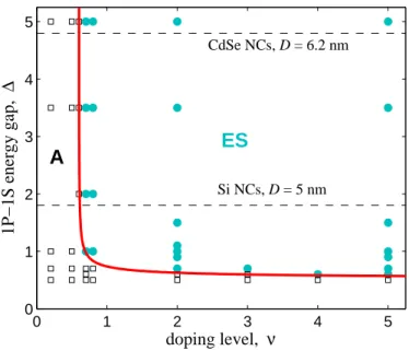
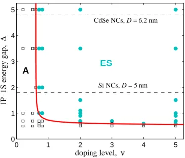
Si NCs, D = 5 nmFigure 1.3: (Color online) Phase diagram indicating regimes of activated and ES re-sistivity as a function of doping level ν and the dimensionless quantum energy gap ∆ ≡ 20.64κaB/κNCD at low temperature kBT ≪ e2ξ/κD2. Symbols correspond to
simulated systems: filled (light blue) circles indicate systems that exhibited ES resis-tivity and open squares indicate systems that exhibited activated resisresis-tivity. The thick (red) curve is an approximate boundary between these two regimes, which are labeled “ES” and “A”, respectively. Dashed, horizontal lines indicate the value of ∆ corre-sponding to Si NCs withD= 5 nm (as in Ref. [27]) and to CdSe NCs withD= 6.2 nm (as in Ref. [4]). This phase diagram and the computer simulation methods are discussed more thoroughly in Ch. 2.
NC, the NC diameter D, and the temperatureT satisfy the following three conditions:
(i) ν &0.6,
(ii) D.34κaB/κNC, and
(iii) kBT .0.5e2ξ/κD2.
Here, κNC is the internal dielectric constant of NCs. When these three conditions are
satisfied, the resistivity follows the ES law. In situations where any of the three criteria is not met, the conduction is activated. This result is depicted at low temperature,
In contrast to semiconductor NCs, where the spontaneous charging is driven by ran-dom doping and relatively large quantum gaps, metallic NCs are different in two ways. First, in metallic NCs the gap ∆ between quantum energy levels becomes vanishingly small and spontaneous charging does not occur. Second, disorder now comes from a different source. Instead of fluctuations in donor number among dots, in such systems disorder is provided by donors and acceptors that are randomly situated in the intersti-tial spaces between grains—for example, in the metal oxide of the grains (more details about the disorder mechanism are discussed in Ch. 3). It is then an interesting question to see how the DOGS and conductivity of the system are going to be modified.
−2 −1 0 1 2 3 0 0.2 0.4 0.6 0.8 1 1.2 density of states, g*( ε ) electron energy, ε 10−2 100 10−4 10−2 100 102 |ε| g*( ε )
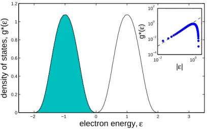
Figure 1.4: (Color online) The DOGS of a regular 3d array of monodisperse NCs, where
ε=E/(e2/2C0) is the dimensionless single-particle energy andg∗(ε) = (e2Dd/2C0)g(ε)
is the dimensionless DOGS, where D is the NC diameter. Here, the results are shown from a computer simulation of a 3d cubic lattice. The shaded area shows filled electron states, and the empty area indicates empty states. In addition to electron–hole symme-try, the two peaks of the DOGS have a mirror symmetry across ε = ±1, respectively (dotted lines). This symmetry creates from the central Coulomb gap two additional half-gaps at ε = ±2, resulting in a “Coulomb gap triptych.” Insets show the DOGS near the Fermi level ε= 0 in log-log scale.
In Ch. 3, we explore hopping transport in two-dimensional (2D) and three-dimensional (3D) arrays of monodisperse normal metallic grains. The most striking result is the re-peated Coulomb gap in the DOGS. We show that, as a result of the periodic charging spectrum of individual grains, there is not one but three identical adjacent Coulomb gaps
in the DOGS (one full gap at the Fermi level and two “half-gaps” on either side), which together form a structure that we termed a “Coulomb gap triptych.” The Coulomb gap triptych represents a bridge between the concepts of the Coulomb gap and the Coulomb blockade. In addition, the DOGS in metallic granular arrays exhibits a rather surprising feature: unlike in conventional Coulomb glass models, it has a fixed width in the limit of large disorder. This result is shown in Fig. 1.4, which can be verified by tunneling experiments.
The final type of NC arrays to be discussed is periodic arrays of superconducting grains in the strongly disordered limit, where the array of superconducting grains as a whole is insulating while individual grains may still contain Cooper pairs. Coherent tunneling of Cooper pairs (the Josephson effect) is neglected. In such a system, elec-tronic states are localized and electron conduction proceeds primarily by hopping of electrons between grains through the insulating gaps which separate them.
At a given temperatureT, two important energy scales associated with the spectrum of electron energy states within each grain affect the magnitude of hopping conductivity . The first one is the charging energyEc=e2/2C0, whereC0 is the self-capacitance of a
single grain. The second energy scale is the superconducting gap ∆0, which represents
an activation energy for separating a Cooper pair. In the limit where ∆0/Ec → 0,
the array is equivalent to a granular metal [5, 28, 29, 30]; in the opposite limit, each grain has the properties of a bulk superconductor. Here, we are interested in the regime when Ec and ∆0 are similar in magnitude. The previous study of metallic NCs can be
considered as a model for a granular superconductor in the limit where ∆0/Ec→0.
In principle, electronic conduction can occur either through tunneling of single elec-trons or through simultaneous tunneling of an electron pair (or both). Using a simple computer simulation, we show that it is the ratio of superconducting gap to charging energy ∆0/Ec that determines whether the hopping transport is governed by tunneling
of single-electrons or electron pairs. Specifically, we study the DOGS and conductivity as a function of gap ∆0and temperatureT. The result for the DOGS of single electrons,
which is denoted g1(ε), is shown in Fig. 1.5(a) for different values of ∆∗= ∆0/Ec. Fig.
1.5(b) shows the DOGS for electron pairs,g2(ε). As ∆∗grows, the system switches from
single-electron dominated regime to electron pair dominated regime. The transition is also reflected in system’s hopping conductivity, which is discussed thoroughly in Ch. 4.
−2 0 2 4 −4 0 0.2 0.4 0.6 0.8 1 1.2 electron energy, ε DOGS, singles, g1 *(ε ) −4 −2 0 2 4 −6 −8 6 8 0 0.2 0.4 0.6 electron energy, ε DOGS, pairs, g2 *(ε ) ∆* = 0 ∆* = 0.5 ∆* = 1 ∆* = 1.5 ∆* = 0 ∆* = 0.5 ∆* ≥ 1 a) b)
Figure 1.5: (Color online) Single electron and pair DOGS, g1∗(ε) andg∗2(ε), of a regular 2d array of monodisperse metallic grains as a function of the dimensionless electron energy ε = E/Ec at different values of the superconducting gap ∆∗ = ∆0/Ec. At
∆∗ < 1, the single electron DOGS g∗1 has a soft Coulomb gap at ε = 0, while the pair DOGS g2∗ has a hard gap, and the situation is reversed for ∆∗ > 1. ∆∗ = 1 is a critical point at which both g∗1,2 have a soft Coulomb gap. The three DOGS curves corresponding to g1∗(ε) at ∆∗ = 0,1 and g2∗(ε) at ∆∗ ≥ 1 constitute “Coulomb gap triptychs” and can be scaled onto each other by rescaling the electron charge.
The mechanism of the giant magnetoresistance peak observed in many superconducting thin films can also be qualitatively explained by the evolution of DOGS.
In the remainder of this thesis, we turn our attention from NC assemblies to another important type of disorder system: 3D topological insulators. As briefly discussed in the previous section, the bulk of a 3D TI is essentially a heavily-doped, strongly compensated semiconductor, with a large number of charged dopants present in the bulk. These impurities create enormously-fluctuating random Coulomb potential that bend the conduction and valence bands, and the bulk resistivity can be dramatically different from the one assumed in the flat bands picture of TI [31]. First, at relatively high
Ee Eh Ec Ev Rg Eg
û
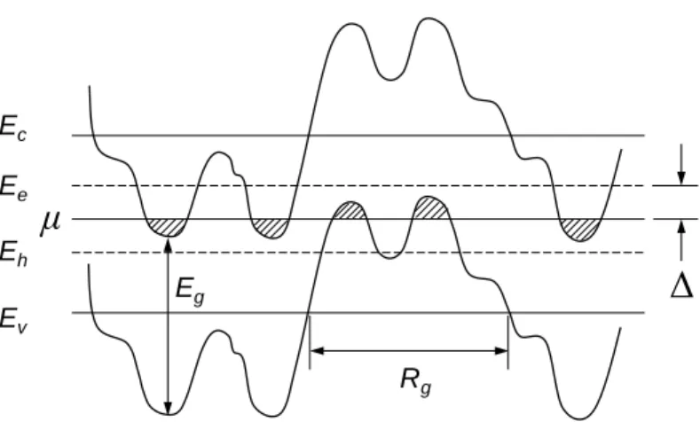
Figure 1.6: Energy diagram of a completely compensated TI with band gap Eg. The
upper and the lower straight lines (EcandEv) indicate the unperturbed positions of the
bottom of the conduction band and the ceiling of the valence band; the middle line (µ) corresponds to the Fermi level. Meandering lines represent the band edges, which are modulated by the fluctuating potential of charged impurities; Rg is the characteristic
size of these potential fluctuations. The percolation levels for electrons, Ee, and holes,
Eh, are shown by dashed lines; the activation energy ∆ corresponds to the difference
Ee−µ(or µ−Eh). Puddles occupied by carriers are shaded. Shallow impurity levels
are not shown because they merge with the band edges.
temperatures activated conduction is due to electrons and holes being activated from the Fermi level to their corresponding classical percolation levels (classical mobility edges),
Ee andEh, in the conduction and the valence bands. These may be substantially closer
to the Fermi levelµthan the unperturbed by random potential bottom of the conduction band Ec and ceiling of the valence bandEv (Fig. 1.6). 1 Thus, one can think of the
universal small factor ∆/Eg ≃15 as corresponding to a percolation threshold associated
with percolation through the potential created by random impurities in 3D. Second, at low enough temperatures electrons and holes can hop (tunnel) between puddles, so that variable range hopping replaces activated transport. In the low temperature limitρ(T) should obey the ES law of VRH [3].
The above theory on the enhanced bulk conductivity in TI was confirmed by numer-ical simulations using percolation approach. We compute the resistivity as a function
1 Note thatE
chere represents the bottom of the conduction band, and should not be taken as the
of temperature, and find two activated regimes of hopping conductivity. At high tem-peratures we see the large activation energy Ea∼Ec−µ; in the range of intermediate
temperatures, we see much smaller activation energy ∆≃0.3(Ec−µ) = 55 meV, which
is in good agreement with the experimental value. At low temperatures the resistivity is well described by ES law.
So far we have focused on the case of complete compensationK= 1. In the remain-der of Chapter 5, we move on to a more practical situation: a strongly compensated semiconductor (SCS), namely 1−K ≪ 1. This is because with existing methods of growth of TI samples one cannot reach K = 1 exactly. It is then important to know how stable the resistivity results at K = 1 are for the case of 1−K≪1.
We model numerically the ground state of such SCS and its resistivity using algo-rithms similar to Ref. [31]. We find that in agreement with the analytic theory [32], when 1−K grows, the screening of the random potential improves and its correlation length Rg decreases. The amplitude of the random potential decreases as well. As a
result, hole puddles shrink and eventually vanish and the chemical potential µ moves up, so that Ec−µ decreases. One can say that with increasing 1−K, the screening
due to bending of the conduction band occurs only while all acceptors remain occupied by electrons and negatively charged.
0.2 0.3 0.4 0.5 0.05 0.1 0.15 0.2 (Ec − µ)/Eg activation energy, ∆ /E g ∆∼ 0.3(Ec − µ)
Figure 1.7: (Color online) The activation energy ∆ at K = 1,0.99,0.98,0.97,0.96 and 0.95 (from right to left). The dashed line is the best linear fit ∆≃0.3(Ec−µ).
We find that the relation ∆ = 0.3(Ec−µ) obtained in Ref. [31] for K= 1 remains valid
for 1−K ≪ 1 (see Fig. 1.7) as well. [In p-type semiconductor where K =ND/NA, a
similar relationship ∆ = 0.3(µ−Ev) takes place.] In principle, our prediction that ∆ =
0.3(Ec−µ) can be directly compared with experiments in TIs. Indeed, for eachK, the
position of the Fermi level can be found via measurements of the surface concentration of electrons in the gapless surface state using Shubnikov-de-Haas oscillations.
Chapter 2
Semiconductor Nanocrystals
2.1
Introduction
Arrays of semiconductor NCs have great promise for optoelectronic and photovoltaic devices, for both their optical and electronic properties can be readily tuned – the former by choosing the size or shape of NCs [27, 33], and the latter by the addition of dopants or surface ligands that control the spacing between NCs [34, 35]. Recent experiments have demonstrated that dense, crystalline arrays of spherical semiconductor NCs can be reliably produced with diameter in the range 4–10 nm and with less than 5% dispersion [27, 28]. Thus, optoelectronic or photovoltaic devices made from NCs can be designed to operate precisely in any chosen region of the optical spectrum.
In Fig. 2.1(a), for example, a high-resolution tunneling electron microscope image of a single CdSe NC is shown, where the dark spots are CdSe atoms aligned periodically just like in a bulk crystal. NCs made from PbSe or Si are also commonly studied. As produced, due to a variety of forces such as the van der Waals internaction, individual NCs can self-assemble themselves into a superlattice. Fig. 2.1(b) shows a face-center cubed superlattice of CdSe NCs. Such a superlattice combines both individual and collective properties of NCs and may give a range of interesting physical phenomena.
From a practical standpoint, however, the development of NC-based devices is slowed by the high resistivity of the NC arrays. In their undoped state, semiconductor NCs are insulators, and in order to reduce their large resistivity it is necessary to bring additional electrons (or holes) to the NCs either through chemical doping [36] or electrochemical
Figure 2.1: Transmission electron microscopy of (a) a single CdSe NC and (b) a face-center cubed superlattice of CdSe NCs.
gating [4]. In this chapter we focus primarily on the former, although we comment on electrochemical gating at the end of the chapter.
In particular, we consider the case where each NC is made from a semiconductor that is heavily-doped by donor impurities. In this case all donor electrons reside in the conduction band of the NC. In order to conduct across the array, these electrons must tunnel between NCs under the high barrier associated with the insulator (such as the ligands shown in Fig. 2.2) that fills the space between them.
In the presence of even a relatively small amount of disorder in the array, the large tunneling barriers imply that donor electrons experience Anderson localization due to fluctuations in the electron energy from one NC to another [1]. In this situation con-duction proceeds only by phonon-assisted tunneling, or “hopping”, between localized electron states. This hopping is a thermally-activated process in which electron tunnel-ing occurs simultaneously with the absorption or emission of a phonon whose energy accounts for the difference between the initial and final electron states. (While metallic conduction through the array is in principle possible, and has been reported [37], it requires the characteristic disorder energy in the system to be smaller than the hopping integral t between neighboring NCs. Sincet decays exponentially with the separation
d between NCs and with the height of the tunneling barrier them, the condition for metallic conductivity is difficult to meet, and in this chapter we assume that electron conduction proceeds by hopping.)
D
d
D’
Figure 2.2: (Color online) Schematic drawing of spherical semiconductor NCs (large, light-colored circles) with diameterD arranged in a crystalline lattice with lattice con-stant D′. Each NC is coated in a thin layer of insulating ligands (curvy lines) that maintain a separationd=D′−Dbetween NCs and prevent them from sintering. Each NC has a random number of donors in its interior (small, black circles).
hopping transport requires an electron to be thermally excited to jump from one neutral NC to another. This process produces two oppositely charged NCs, each of which has a corresponding Coulomb self-energy Ec = e2/κD, where κ is the effective dielectric
constant of the NC array and D is the NC diameter. This charging energy plays the role of an activation energy for resistivity in the case where all NCs are neutral in the global ground state. Equivalently, one can say that the distribution of electron ground state energies, or the “density of ground states” (DOGS) of NCs, has a gap of width 2Ec
centered at the electron Fermi level, as shown in Fig. 2.3. As a result, the resistivity
ρ follows the Arrhenius law: lnρ ∝ Ec/kBT, where kBT is the thermal energy. We
emphasize that the activation energy for hopping conduction is sensitive only to the
ground state energies of electrons and holes that are added to NCs. For this reason
when calculating the resistivity it is sufficient to consider the DOGS, which does not include excited electron states with additional kinetic energy.
In experiments, however, one often observes a temperature dependence of the re-sistivity that is different from simple activation: lnρ ∝ T−γ, with the temperature
Figure 2.3: (Color online) Distribution of electron ground state energies in the absence of any disorder. The bottom shaded (green) peak corresponds to the filled states, while the top empty one corresponds to the excited states. The DOGS has a gap of width 2Eccentered at the electron Fermi level.
exponent γ <1. Such “stretched exponential” behavior is believed to be possible only if the disorder is so strong that a substantial fraction of NCs is charged in the global ground state. Such charging creates a random Coulomb potential landscape that shifts up and down the electron energy spectra at different NCs. As a result of this shifting, the gap in the DOGS is smeared and filled. This smearing means that some electron states have energies very close to the Fermi level, and as a result one can find a pair of empty and filled electron states separated by an energy ∆E that is much smaller than
Ec. At small temperaturekBT ≪Ec, it is hopping between such pairs that are close in
energy that dominates the conduction.
Of course, for small ∆E the typical separationrbetween the corresponding NC pair is much larger than the spacing D′ between neighboring NCs. Thus, at small temper-ature T electron conduction relies on tunneling between distant NCs. To understand how such long-range tunneling is possible, consider first the tunneling of an electron be-tween nearest-neighboring NCs. When the electron tunnels through the insulating gap of thicknessdbetween NCs, it accumulates an action~d/a, whereais the decay length of the electron wavefunction outside of the NC. Thus, the tunneling amplitude between nearest neighbors is suppressed by a factor ∼exp[−d/a]. On the other hand, when an electron tunnels to a NC at a distance x ≫ D′, the path of least action for the elec-tron is to travel primarily through nearest-neighboring NCs, making hops only through the small gaps between neighbors and thereby accumulating an action∼~(d/a)(x/D′), plus an additional much smaller term corresponding to action accumulated across the
interior of each NC. Thus, the tunneling amplitude to the distancexis suppressed by a factor ∼exp[−xd/D′a]. The exponential decay of the tunneling amplitude is described by defining the localization length ξ, such that tunneling between NCs with separation
r is suppressed by the factor exp[−2r/ξ]. By the argument above, one cannot simply equateξ witha, but ratherξ ∼aD′/d≫a[29]. It is this enhanced localization length, made possible by tunneling through intermediate NCs, that allows for long-range hop-ping. In the remainder of this chapter, we consider the limit where dand a are both very small compared to the NC diameter, so that D′ ≃Dwhile ξ remains finite.
If the temperatureT is made increasingly small, the corresponding energy difference ∆E of electron hops becomes increasingly small due to the scarcity of available high-energy phonons, and as a result the typical hop length increases. Such behavior is known as variable range hopping (VRH), and is responsible for the stretched exponential behavior γ <1 in the resistivity. When the DOGS is constant near the Fermi level, the resistivity follows the Mott law of VRH [2]: lnρ ∝T−1/4. However, in systems where the long-ranged Coulomb potential is not screened, electron correlation effects produce a DOGS that vanishes quadratically with energy at the Fermi level [3]. Such a vanishing DOGS results in the Efros-Shklovskii (ES) law of VRH: lnρ ∝T−1/2. In principle, all three of these conduction behaviors — Arrhenius (γ = 1), Mott VRH (γ = 1/4), and ES VRH (γ = 1/2) — are possible in arrays of semiconductor NCs, depending on the magnitude and type of disorder present. In this chapter we focus our description on the fundamental role played by inherent fluctuations in donor number among doped NCs.
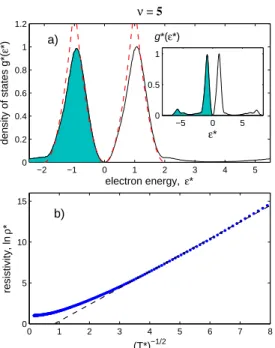
Experiments probing the resistivity of NC arrays have reported that the resistivity depends in a sensitive and qualitative way on the level of doping [4]. Specifically, as the average numberνof dopant electrons per NC is varied, the dependence of the resistivity
ρ on the temperatureT changes between Arrhenius-type activated conduction (γ = 1) and VRH (γ < 1). VRH has been reported in a variety of granular semiconductor systems [4, 33, 38, 39], but thus far there is no general theory to explain how these different types of conduction can coexist and why they appear in particular ranges of the electron “filling factor” ν.
In this Chapter we present such a theory, based on a first-principles description of the ground state arrangement of electrons within an array of doped NCs. We focus on a simple model of identical spherical NCs that are covered by a thin layer of insulating
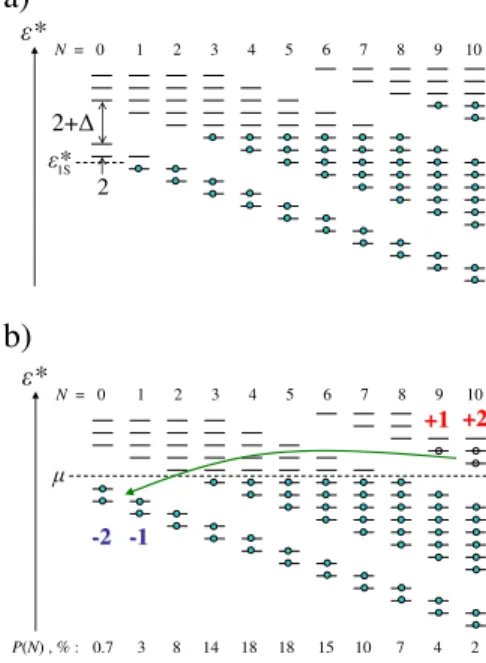
ligand (or some other insulator) and arranged in an ideal crystalline lattice, as depicted in Fig. 2.2. We show that the presence of fluctuations in donor number between different NCs is sufficient to produce charging of NCs, which results in a disordered Coulomb landscape that encourages VRH. This charging is driven by the large gaps between shells of the electron quantum energy spectrum in NCs with large Bohr radiusaB. Specifically,
these inter-shell gaps drive electrons to depart from NCs with a large number of donors, where maintaining electroneutrality would require placing electrons in higher quantum energy shells, and reside instead on nearby NCs with small donor number. In this way some NCs spontaneously acquire a positive or negative charge, and it is this charging that leads to VRH when the temperature is not too large.
Using this model, we explain how the different regimes of resistivity observed in experiment arise based on the interplay between the charging spectrum of NCs, the long-ranged Coulomb interactions between charged NCs, and the discrete quantum en-ergy levels of confined electrons. We supplement our theory with a simple computer simulation, which we use to calculate the DOGS and the resistivity.
Ch. 2 is organized as follows. In Sec. 2.2 the theoretical model for semiconductor NCs is defined. Sec. 2.3 describes our computer simulation, including our methods for numerically calculating the DOGS and resistivity. Results are presented in Sec. 2.4, along with a discussion of why Arrhenius and VRH resistivity appear in particular regimes ofν,D, andT. We also discuss interesting features of the DOGS in this model, including the appearance of “reflected Coulomb gaps” at either side of the Fermi level. Sec. 2.5 presents some speculation on how our results can be applied to electrochemical gating of NC arrays using ionic liquids followed by concluding remarks in Sec. 2.6.
2.2
Model of NC arrays with random number of dopants
In order to describe the resistivity of a dense array of semiconductor NCs and capture its dependence on doping level, temperature, and NC diameter, we adopt the following simplified theoretical model. We consider NCs to be identical spheres of diameter D
with large internal dielectric constantκNC≫κ. These spheres are arranged in a regular,
three-dimensional (3D) lattice, with each lattice siteilocated at the center of a NC. For simplicity, we consider a cubic lattice with lattice constant D′ just barely larger than
D, so that d ≪ D (see Fig. 2.2). Our choice of a cubic lattice does not qualitatively affect any of the results we present below.
We further assume that the radiusD/2 of the NCs is comparable to or smaller than the effective electron Bohr radiusaB=~2κNC/me2of the semiconductor, whereeis the
electron charge andmis the effective electron mass. As an example, NCs made from Si have aB ≈2.4 nm; for CdSe NCs, aB ≈5 nm. Under this condition the wavefunction
of a donor electron is extended across the entire volume of a NC, rather than localized around a donor impurity, and the energy of the electron is strongly affected by quantum confinement within the NC. As an example, a single donor in the center of a NC has a delocalized electron state when D < 6aB [40, 41]. This condition can be used as
a somewhat conservative estimate for how small the diameter should be to produce electron states that are extended across the NC.
In order to obtain the quantum energy spectrum in NCs, one can make the approx-imation that each NC is an infinite 3D square well. Such an approxapprox-imation is valid because of the NCs’ relatively large work function. The resulting energy spectrum can be described by defining the energy EQ(n) of the nth lowest electron, which gives for
the first few energy levels
EQ(n) = ~ 2 mD2 × 0, n= 0 19.74, n= 1,2 40.38, 3≤n≤8 66.43, 9≤n≤18 . (2.1)
These first three nonzero energy levels can be labeled 1S, 1P, and 1D, respectively. Higher electron shells have thus far not been examined by experiment, since they corre-spond to very large doping, and will not be discussed in this work. We focus primarily on the case where the spacing between quantum energy levels ≈ 20~2/mD2 is larger
than the characteristic scale of Coulomb energies, e2/κD. The expression of Eq. (2.1) ignores the weak perturbation of quantum energy levels resulting from electron-electron interactions. This approximation is justified because of the large internal dielectric constantκNC, as explained below.
During the doping process, each NCiacquires some numberNiof positively-charged
donors that it contains within its interior. These are assumed to be fixed, while the number of electrons ni within the NC can change due to electron tunneling between
NCs. We assume that donors are added randomly to each NC by some high-temperature process, so that if the average number of donors per NC is ν, then the probability that a given NC will have exactly N donors is given by the Poisson distribution:
P(N) = ν
N
N!e
−ν. (2.2)
This randomness in the number of donors is the only form of disorder that we include in our model. We show in Sec. 2.4 that this disorder is sufficient to produce random charging of NCs, which leads to VRH. As mentioned in the introduction, the spontaneous charging of NCs is the result of the large gaps between quantum kinetic energy shells, which drive electrons away from NCs with many donors (emptying higher shells) and into NCs with few donors (filling lower shells), so that the number of electrons in a given NC is not generally equal to the number of donors. Additional disorder arising from fluctuations in the NC size is not considered explicitly in this chapter. The possible effect of such size fluctuations is discussed at the end of Sec. 2.4, but we note here that fluctuation of NC size alone cannot produce spontaneous charging of NCs in the global ground state, which, as we show below, plays a crucial role for VRH.
In addition to the quantum kinetic energy of the system, transport through the ar-ray is also greatly affected by long-ranged Coulomb interactions, which must be taken into account. In general, one could expect that calculating the total Coulomb energy of the system is a difficult problem, since the positions of negative electrons within each NC are described by their corresponding quantum wavefunctions and the positions of positive donors are random within the NC’s volume. For our problem, however, a sig-nificant simplification is available because the internal dielectric constant κNC is much
larger than both the external dielectric constant κi of the insulator in which the NCs
are embedded and the overall effective dielectric constant κ of the assembly. Specif-ically, the large internal dielectric constant κNC implies that any internal charge e is
essentially completely compensated by the dielectric response, with the great majority of that charge, e(κNC−κ)/κNC, becoming distributing across the surface of the NC.
In this way each NC can be thought of as metallic in terms of its Coulomb interac-tions. This allows us to write that the Coulomb self-energy of a NC with net charge
are arranged. The interaction between two NCs i, j at a distance rij can also be
ap-proximated asqiqj/κrij. These approximations are equivalent to the so-called constant
interaction model, which is commonly used for individual quantum dots [42].
It should be noted that the effective dielectric constant κ of the NC array is not simply equal to the dielectric constant κi of the insulating medium between NCs, but
also includes the effect of polarization of NCs in response to an applied field. This polarization effectively decreases both the Coulomb self-energy of a single NC and the interaction between neighboring NCs. Generally speaking, the renormalization of the dielectric constant is not very strong, so that κ is not very different from κi even when
κNC≫κi. The canonical Maxwell-Garnett formula gives the approximate relation [43]
κ≃κi
κNC+ 2κi+ 2f(κNC−κi)
κNC+ 2κi−f(κNC−κi)
, (2.3)
where f =πD3/[6(D′)3] is the volume fraction occupied by the NCs; for f <0.4, this expression is accurate to within 8% [44]. As an example, for the case of a cubic lattice withD= 5 nm andD′ = 6 nm (so thatf = 0.3) and forκNC/κi= 5, one hasκ≈1.6κi.
Given this model, we can write down the Hamiltonian for our system as
H = ∑ i [ e2(Ni−ni)2 κD + ni ∑ k=0 EQ(k) ] +∑ ⟨i,j⟩ e2(N i−ni)(Nj−nj) κrij . (2.4)
Here, the first term describes the electrostatic self-energy of NC i, which has charge
qi=e(Ni−ni), the second term describes the total quantum energy of the ni electrons
on NC i, and the last term indicates the Coulomb interaction between different NCs. The ground state for a particular system (a set of donor numbers {Ni}) is defined
by the set of electron occupation numbers {ni} that minimizes the Hamiltonian H.
Given the ground state configuration, one can determine the energy of the highest filled electron level, ε(if), and the lowest empty electron level, ε(ie), at each NC i. Specifically,
ε(if) = EQ(ni) + e2[(Ni−ni)2−(Ni−ni+ 1)2] κD −∑ j̸=i e(Nj−nj) κrij (2.5)
and ε(ie) = EQ(ni+ 1) + e2[(Ni−ni−1)2−(Ni−ni)2] κD −∑ j̸=i e(Nj−nj) κrij . (2.6)
For the global ground state configuration, ε(if) < ε(je) for all i, j. As alluded to in the introduction, the definitions ofε(if) andε(ie) describe only the lowest energy state of an electron or hole added to the site i. For this reason we refer to the density of states of these energy states ε(ie,f) as the DOGS.
The resistivity of the NC array is largely determined by the set of these ground state single-particle energies {ε(if)} and {ε(ie)}. In the following section we show how these energy states can be used to calculate both the ground state electron DOGS g(ε) and the resistivityρas a function of temperature and doping level. Note that in this problem every site is represented by two energies, in contrast to the canonical impurity band of lightly-doped semiconductors [32], where every donor has only one relevant excitation energy.
It is also important to note that in our model these donor electrons are assumed to be responsible for all conduction. In other words, we assume that the temperatureT is low enough (and the doping levelνis high enough) that donor electrons are much more abun-dant than electrons activated from the valence band. In practical cases, this assumption is easily met: it requires only that the thermal energy kBT be much smaller than the
band gap energyEg. More exactly, it requires that kBT ≪Eg/ln[κNCD2Eg/e2aBν2/3].
2.3
Computer modeling
In this section we describe our computational method for calculating the density of states and the resistivity at a given value of ν, T, and D. These calculations are based on a computer simulation of a finite, cubic array ofL×L×LNCs, which proceeds as follows. First, we specify the doping levelν. The simulation then assigns the donor numberNi
for each NC i according to Eq. (2.2). The initial values of the electron numbers {ni}
are then assigned randomly in such a way that the system is overall electro-neutral, i.e.,
∑
ini =
∑
NC pairs ⟨ij⟩ and attempting to move one electron fromi toj. If the move lowers the Hamiltonian H, then it is accepted, otherwise it is rejected. Equivalently, one can say that for each pairi, j we check that two ES ground state criteria are satisfied:
ε(je)−ε(if)− e 2 κrij >0 (2.7) and ε(ie)−ε(jf)− e 2 κrij >0. (2.8)
If either one of these criteria is violated, then an electron is transferred. This process continues until all sites i, j satisfy Eqs. (2.7) and (2.8).
It should be noted that this procedure does not in general find the exact ground state, but only a “pseudo-ground state” that is stable with respect to single-electron transfers. In principle, the system energy can be lowered further by some multi-electron transfers. The effect of these higher-order relaxation processes on the properties of the pseudo-ground state has been examined for similar models [45, 46], and they are generally beyond our intended accuracy in this chapter, so we do not consider them here.
Once the pseudo-ground state occupation numbers {ni} have been found, one can
define the single-particle energiesε(if) and ε(ie) for each NC iusing Eqs. (2.5) and (2.6). These energies are tabulated and then histogrammed in order to calculate the single-particle DOGSg(ε). In the results presented below we define electron energiesεrelative to the Fermi level µ, which is calculated for each realization of the simulation as µ = [min{ε(ie)} −max{εi(f)}]/2. In this way ε < 0 corresponds to filled electron states ε(f)
while ε >0 corresponds to empty statesε(e). (See, for example, Fig. 2.5 below.) Once the pseudo-ground state energies{ε(if)}and{ε(ie)}are determined, we calculate the resistivity of the system by mapping the simulated NC array to an effective resistor network. The equivalent resistance Rij between NCs i and j can be determined by
writing down the time-averaged rate of electron transfer between sites i and j in the presence of an electric field and expanding in the limit of small field, as in the canonical Miller-Abrahams resistor network [32, 47]. In calculating Rij we consider only electron
transfer among the highest filled states, ε(f), and the lowest empty states, ε(e), which is appropriate when the temperature is small enough thatT < e2/κD, so that thermal excitation of multi-electron transitions is exponentially unlikely.