network
1
Soumaya Azzouni,
2Nizar Khitouni,
3Med Salim Bouhlel
1PhD student, Sciences of Electronics Technologies of Information and Telecommunications, higher institute of biotechnology of sfax, Route de Soukra km 4, BP
261 3000, Tunisia.
2Professor, Sciences of Electronics Technologies of Information and Telecommunications, higher institute of biotechnology of sfax, Route de Soukra km 4, BP 261 3000, Tunisia.
3Professor, Sciences of Electronics Technologies of Information and Telecommunications, higher institute of biotechnology of sfax, Route de Soukra km 4, BP 261
3000, Tunisia.
Correspondence Author: Nizar Khitouni, University of Sfax, Sciences of Electronics Technologies of Information and Telecommunications, higher institute of biotechnology of sfax Route de Sokra km 4 BP. 261 3000 Tunisia
E-mail: [email protected]
Received date: 15 April 2018, Accepted date: 15 June 2018, Online date: 15 July 2018
Copyright: © 2018 Nizar Khitouni et al. This is an open-access article distributed under the terms of the Creative Commons Attribution License, which permits unrestricted use, distribution, and reproduction in any medium, provided the original author and source are credited.
Key words: Analog-digital, Sigma‐delta modulation, continuos, RF, LTE.
INTRODUCTION
The digital processing performance of signals and communication systems is generally limited by the quality of the input signal (resolution) (Gabriel ANTONESEI et al., 2010). The increasing use in telecommunication digital technique, Long Term Evolution (LTE), like audio applications, supported the analog to digital converter use. With increasing development of LTE (Long Term Evolution) communication application and signal acquisitions, there is a great demand to request signal bandwidths of some megahertz for analog-to-digital converters (ADCs) in the wireless communication.
Forthcoming communication standards like LTE-A specify transmission scenarios using signals with up to 100 MHz bandwidth (Kelly Tchambake et al., 2017) However, it proved that the traditional converters do not reach high performances on a small surface.
Current research in the field of telecommunication progress exceeds the current technological limits and improves the concept of the future system performances considerably: better integration rate, low power, personal communication apparatus size reduced and the capacity of multiplying the communication number. For the signal transmission, we use a conversion technique called modulation such as the coded pulse modulation or the Sigma-delta modulation. The Sigma- delta (ΣΔ) conversion is currently an increasingly widespread technique in the field of Analog/digital conversion. The analog to digital sigma-delta modulation presents a compromise between the high resolution, (more than 12 bits) and the high integration. Although the ΣΔ modulator was introduced in (Xu Y
et al., 2010) (R. Suszyński et al., 2013), it did not earn importance until a recent development of the VLSI technology which allows the implementation on much reduced surfaces. Moreover, these converters are simple, robust and well adapted to the high-speed applications. The converters guarantee a high resolution and can be easily implemented on a chip: it is a concept key to improve the communication system performance and to allow the third generation air interface realization. To improve the resolution and accuracy, the converter (A/D) is built of two different structures to convert N most significant bits (MSBs) and M least significant bits (LSBs), respectively (K. Wawryn et al 2013). This paper is organized as follow. Section II introduces the receiver architecture, including the description of LTE Network. In Section III, the modulator topology and the architecture proposed are presented. Finally, Simulation results and conclusions are given in Section IV and Section V, respectively.
2. Reception Chain:
The Radio Frequency receiver chain is generally constituted by: an antenna, a low noise amplifier, mixer, filters and analog-to-digital converter. An ADC is an electronic structure that transforms the DC signal into a series of discrete numerical values. The main characteristics of the ADC are resolution, sampling frequency, linearity and consumption. The receiver lowers the RF frequency to a lower intermediate frequency to facilitate information retrieval. Generally, there are three main families of receiver architecture. Depending on the intermediate frequency value: Heterodyne Receiver, Homodyne Receiver, and Low Intermediate Receptor. The heterodyne architecture is the oldest and used for most cell phones in the past. It is called Superheterodyne when transposing frequency into several steps. The principle of this architecture is presented in the figure, it begins by filtering the RF signal received by a band selection filter and then amplifying it by a low noise amplifier (LNA), then filtered by a rejection filter images. The IR filter output is converted to the intermediate frequency (IF) via a mixer. Then a channel filtering is performed. A homodyne receiver is also referred to as direct conversion or Zero-IF. This architecture has a simpler structure than that of the heterodyne receptor. The principle consists of transposing the baseband signal directly using an IQ block. The resulting baseband signal is then filtered before passing through the ADC.
Abstract
Fig. 1: Architecture of a homodyne receiver.
The low-frequency intermediate receiver architecture is based on the same principle of the homodyne receiver, the transposition of RF signal in the baseband, to a non-zero but fairly low intermediate frequency. This reintroduces the problem of image frequency that can removed by an image suppression technique. Each receiver architecture has major advantages and disadvantages. The simplest architecture is aimed at with low cost and low energy consumption. The heterodyne receiver offers high selectivity and sensitivity but suffers from the image frequency problem. The use of the various filters to respond to this problem increases the complexity of realizing a system especially at high frequencies. The high number of components increases energy consumption and makes it difficult to adapt to the system requirements of a single integrated chip required by communication systems today. The same image frequency problem occurs in the low-frequency intermediate architecture. The choice of the homodyne architecture is justified by the simplicity, absence of image frequency problem that the addition of filters and convenience with systems on chips require. However, this architecture has disadvantages that can be alleviated by the implementation of different methods (MAK et al., 2007).
3. LTE Network:
LTE (Long Term Evolution) is the name of a project within the third Generation Partnership Project (3GPP) under release 8 name to produce the fourth generation (4G) mobile network standard technical specifications. In fact, it is a system that aims to improve the performance of third-generation networks, and it increases service delivery and diversification by bringing about significant changes. This evolution brings many technical advantages for cellular networks. The bandwidth is scalable, ranging from 1.25 MHz to 20 MHz, in order to adapt to the needs of operators of distinct networks with different bandwidth allocations. Release 9 is based on the development of the missing features found in previous releases, while release 10 focuses on the development of "LTE Advanced" (the real 4G) that is included in the family IMT-advanced (International Mobile Telecommunications-Advanced) introduced by the ITU (International Telecommunication Union). The LTE radio interface has introduced a number of new technologies, enabling the efficient use of spectrum and providing much higher data rates. For example, the LTE used Orthogonal Frequency Division Multiplex (OFDM) technology as a signal carrier and the associated access regimes, OFDMA (Single Frequency Division Multiple Access), SC-FDMA (Single Frequency Division Multiple Access) and MIMO (Multiple Input Multiple Output) (DAHLMAN et al., 2013).
With OFDM technology, LTE allows dynamic assignment of number of subcarriers for a user according to the traffic load. With the advantage of flexibility in the use of the frequency band (different sizes including 1.25, 2.5, 5, 10, 15 and 20MHz).
Compared with traditional antenna techniques that improve channel quality, MIMO is an advanced antenna technology that allows multiple parallel transmissions (orthogonal channels) through the use of multiple antennas at the receiver and the transmitter. The increase in quality is proportional to the number of antennas. MIMO is also a spatial diversity technique that increases system capacity and user throughput without transmission energy and no additional bandwidth.
Table 1: LTE Features.
Bandwidth(MHz) 1.4 3 5 10 15 20
Sub-carrier spacing (Khz) 15
Sampling frequency (MHz) 245.76 245.76 245.76 491.52 460.80 491.52
Modulation Scheme QPSK, 16-QAM, 64-QAM
3. Sigma Delta: 3.1. Overview:
The principle of the Sigma-Delta modulator is based on the concept of oversampling and quantization noise shaping, which is introduced by Culter in 1954. However, the first SDM was invented by Inose et al in 1962. The technique of oversampling involves obtaining a sampling frequency higher than the Nyquist frequency (2 * signal bandwidth). This technique requires a large number of samples in order to reduce the quantification error in the signal band.
(1)
With Fs and Fb are the sampling rate and the signal bandwidth respectively.
Quantification noise shaping, Quantification is the process used to associate an analog signal sampled at a discrete level equivalent to a finite number of bits. The quantization noise is the ratio between the actual value and the level that has been associated with it. Noise shaping is the process of filtering quantization errors. This method reduces the power of the quantization error in the frequency band of interest and increases the quantization error power outside that band. The transfer function of this filter is called NTF: Noise Transfer Function. Several architectures are studied in the literature; they are classified according to different strategies:
The nature of the signal: according to this category, there are two types of modulators, depending on the choice of loop filter: LP ΣΔ (low pass) and BP ΣΔ (band pass).
The LP ΣΔ modulators use the integrator as a loop filter, but the BP ΣΔ use resonators. Therefore, analysis and synthesis are the same only difference is the nature of filter. It is possible to obtain a BP ΣΔ from a LP ΣΔ by applying the transformation method LP to BP.
(2)
The Signal to Noise and Distortion Ratio (SNDR) is given by:
(3)
Psignal is the signal power at the output of the modulator, Pnoise and Pdistortions the power of the harmonics.
The dynamic range of the ADC is a measure of the range of input amplitudes for which the structure always operates correctly (JOSÉ M., 2011).
(4)
ENOB (Effective Number of Bits) is the number of actual bits measured by an input signal, the value of this metric is given by [4].
(5)
The ERBW (effective resolution bandwidth) is equal to the frequency that results in a 3 dB reduction in the SNR value. To compare the various converters, we use the value of Merit Factor (FOM: Figure Of Merite) that is calculated by:
(6)
With Pm is the power consumed by the converter.
3.3. Modulator architecture:
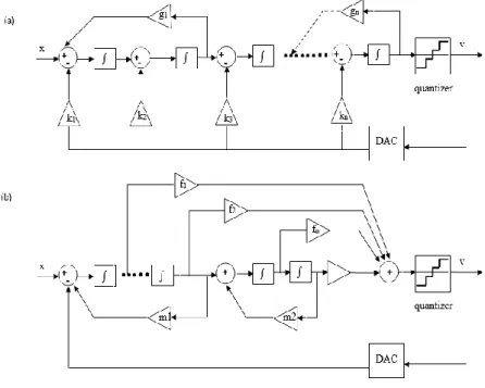
For the same topology, we can implement different implementations. These implementations are generally divided into two main classes (JOSÉ M., 2011): feedback (FB) and feed forward (FF). Each family is presented in Figure 2.
Fig. 2: Architecture (a) Feedback and (b) Feed forward.
The use of internal multibit quantization usually requires linearization techniques in the return DAC. Any error in the level spacing (non-linearity) of a multibit quantizer is directly referenced by the input.
Figure 3 shows the proposed third-order Sigma Delta modulator architecture with single-bit quantizer. The integrators are implanted in the S-domain. On the feedback, NRZ DAC is used with the transfer function (JOSÉ M., 2011).
(7)
Fig. 3: Proposed modulator architecture.
4. Simulation results:
In this section, the simulation results of the proposed architecture are presented using the Simsides (a MATLAB SIMULINK tools). The measured spectrum of the digital output is shown in Fig.4.
In this simulation, the input signal was 2.1 MHz sine wave, and the sampling frequency was 491.52 MHz. The FFT size is 32768 data points and the output data is weighted a Hamming window.
Fig. 4: Measured FFT spectrum.
The continuous-time modulator achieves a DR of 70 dB and an SNR of 69 dB within a 10MHz signal bandwidth. Table 2 summarizes the modulator performance and also lists the comparison with other modulators for wireless networks.
Table 2: Comparison of results.
Ref Fs(MHz) BW(MHz) Order SNR(dB) DR(dB) Technology
XU Ken 2016 491 10 3 62 66
DahlmanErik 2013 240 5 3 70 71 CMOS 90n
Weng C 2017 640 20 4 58 CMOS90n
Ke Y 20110 640 10 4 65 67 CMOS 90n
Crombez P 2010 1000 10 3 43 48 0.35u
Hong J 2014 288 5 3 71 72 65n
Andersson 2012 3000 2
Salgado 2014 80/160/230 2.5/5/10 3 84.8/85.8/84.5 84.6/83.3/81.9 65n
Xu Y 2012 3200 45.7/53.3 3 84.6/83.1 90/88
R.Suszyński 2014 640 10 3 65 67 90n
K. Wawryn 2013 100 1 3 56.8 60
This work 491.52 10 3 69 70 CMOS 0.18u
104 105 106 107 108
-200 -150 -100 -50 0
Mag
n
it
u
d
e
(d
B)
REFERENCES
Andersson, M., M. Anderson, L. Sundström and P. Andreani, 2012. A 7.5 mW 9MHz CT ΔΣ modulator in 65nm CMOS with 69 dB SNDR and reduced sensitivity to loop delay variations. In Solid State Circuits Conference (A-SSCC), IEEE Asian, pp: 245-248.
Crombez, P., G. Van der Plas, M.S. Steyaert and J. Craninckx, 2010., A single-bit 500 KHz-10 MHz multimode power-performance scalable 83-to-67 dB DR CTΔΣ for SDR in 90 nm digital CMOS. IEEE Journal of Solid-State Circuits, 45(6): 1159-1171.
DAHLMAN Erik, PARKVALL Stefan, and SKOLD Johan. 2013 4G: LTE/LTE-advanced for mobile broadband. Academic press. DAHLMAN Erik, PARKVALL, 2013. 4G: LTE/LTE-advanced for mobile broadband. Academic press.
Gabriel ANTONESEI, Cristina TURCU2, Adrian GRAUR. 2010, Basic Consideration for Signal Processing Solutions Used in Sigma-delta Based ADC and DAC Converters, Advances in Electrical and Computer Engineering, 10(1).
Hong, J.H. and Z.Y. Chen, 2014. A low-power 10MHz bandwidth continuous-time ΣΔ ADC with Gm-C filter. In Circuits and Systems (MWSCAS), IEEE 57th International Midwest Symposium on pp: 853-856. IEEE.
José, M., 2011. Sigma-delta modulators: Tutorial overview, design guide, and state-of-the-art survey. IEEE Transactions on Circuits and Systems I: Regular Papers, 58(1): 1-21.
Ke, Y., P. Gao, J. Craninckx, G. Van der Plas and G. Gielen, 2010. A 2.8-to-8.5 mW GSM/bluetooth/UMTS/DVB-H/WLAN fully reconfigurable CTΔΣ with 200kHz to 20MHz BW for 4G radios in 90nm digital CMOS. In VLSI Circuits (VLSIC), IEEE Symposium on pp: 153-154.
Kelly Tchambake, Dang-Kièn Germain Pham, Chadi Jabbour, Patricia Desgreys, Patrick Loumeau, 2017. A Multi-Channel Σ∆ Modulator for Subband Digital Predistortion with LTE signals, IEEE International New Circuits and Systems Conference, 1-4.
MAK, Pui-In, U., Seng-Pan and MARTINS, Rui Paulo, 2007. Transceiver architecture selection–review, state-of-the-art survey and case study. Analog-Baseband Architectures And Circuits For Multistandard And Low voltage Wireless Transceivers, pp: 9-40.
Suszyński, R. and K. Wawryn, 2013. Rapid prototyping of algorithmic A/D converters based on FPAA devices”, Bull. Pol. Ac.: Tech., 61(3): 691-696.
SALGADO, Gerardo Molina, DOLECEK, Gordana Jovanovic, MORGADO, Alonso, et al., 2014. “Design considerations of band pass CT ΣΔ modulators
for software-defined-radio receivers. In Circuits and Systems (ISCAS), IEEE International Symposium on. IEEE, pp: 718-721.
Wawryn, K. and R. Suszyński, 2013. Low power 9-bit pipelined A/D and 8-bit self-calibrated D/A converters for a DSP system, Bull. Pol. Ac.: Tech., 61(4): 979-988.
Weng, C.H., Y.Y. Lin and T.H. Lin, 2017. A 1-V 5-MHz Bandwidth 68.3-dB SNDR Continuous-Time Delta-Sigma Modulator with a Feedback-Assisted Quantizer. IEEE Transactions on Circuits and Systems I: Regular Papers.
XU Ken, CAI Min, DAGHER, Elias H., 2016. A 10.2 mW multi-mode continuous-time ΔΣ ADC with 70–87 dB DR and 0.7–10 MHz bandwidth for TD-SCDMA and LTE digital receivers. Analog Integrated Circuits and Signal Processing, 89(2): 395-410.