The Defi nitive Guide to the
ARM Cortex-M3
The Defi nitive Guide to the
ARM Cortex-M3
Joseph Yiu
AMSTERDAM • BOSTON • HEIDELBERG • LONDON • NEW YORK OXFORD • PARIS • SAN DIEGO • SAN FRANCISCO
SINGAPORE • SYDNEY • TOKYO
Newnes is an imprint of Elsevier
Prelims-H8534.indd iii
Linacre House, Jordan Hill, Oxford OX2 8DP, UK Copyright © 2007, Elsevier Inc. All rights reserved.
No part of this publication may be reproduced, stored in a retrieval system, or transmitted
in any form or by any means, electronic, mechanical, photocopying, recording, or otherwise, without the prior written permission of the publisher.
Permissions may be sought directly from Elsevier’s Science & Technology Rights Department in Oxford, UK: phone: (44) 1865 843830, fax: (44) 1865 853333, E-mail: permissions@elsevier .com. You may also complete your request online via the Elsevier homepage (http://elsevier.com), by selecting “Support & Contact” then “Copyright and Permission” and then “Obtaining Permissions.”
Recognizing the importance of preserving what has been written, Elsevier prints its books on acid-free paper whenever possible.
Library of Congress Cataloging-in-Publication Data
(Application submitted.)
British Library Cataloguing-in-Publication Data
A catalogue record for this book is available from the British Library. ISBN: 978-0-7506-8534-4
For information on all Newnes publications visit our Web site at www.books.elsevier.com 08 09 10 11 12 13 10 9 8 7 6 5 4 3 2 1
Typeset by Charon Tec Ltd (A Macmillan Company), Chennai, India www.charontec.com
Printed in The United States of America
Prelims-H8534.indd iv
Foreword ...
xiii
Preface ...
xiv
Acknowledgments ...
xv
Terms and Abbreviations ...
xvi
Conventions ...
xviii
References ...
xix
Chapter 1 – Introduction ... 1
What Is the ARM Cortex-M3 Processor? ...1
Background of ARM and ARM Architecture ...3
A Brief History ...3
Architecture Versions ...4
Processor Naming ...6
Instruction Set Development ...8
The Thumb-2 Instruction Set Architecture (ISA) ...9
Cortex-M3 Processor Applications ...10
Organization of This Book ...11
Further Readings ...11
Chapter 2 – Overview of the Cortex-M3 ... 13
Fundamentals ...13
Registers ...14
R0 to R12: General-Purpose Registers ...14
R13: Stack Pointers ...14
R14: The Link Register ...15
R15: The Program Counter ...15
Special Registers ...15
Operation Modes ...16
The Built-In Nested Vectored Interrupt Controller ...17
Nested Interrupt Support ...18
Vectored Interrupt Support ...18
Dynamic Priority Changes Support ...18
Reduction of Interrupt Latency ...18
Interrupt Masking ...18
v
Table of Contents
Prelims-H8534.indd v
The Memory Map ...19
The Bus Interface ...20
The Memory Protection Unit ...20
The Instruction Set ...20
Interrupts and Exceptions ...22
Debugging Support ...24
Characteristics Summary ...25
High Performance ...25
Advanced Interrupt-Handling Features ...25
Low Power Consumption...26
System Features ...26
Debug Supports ...26
Chapter 3 – Cortex-M3 Basics ... 29
Registers ...29
General-Purpose Registers R0–R7 ...29
General-Purpose Registers R8–R12 ...29
Stack Pointer R13 ...30
Link Register R14 ...32
Program Counter R15 ...33
Special Registers ...33
Program Status Registers (PSRs) ...33
PRIMASK, FAULTMASK, and BASEPRI Registers ...35
The Control Register ...36
Operation Mode ...37
Exceptions and Interrupts ...39
Vector Tables ...40
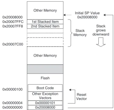
Stack Memory Operations ...41
Basic Operations of the Stack ...41
Cortex-M3 Stack Implementation...42
The Two-Stack Model in the Cortex-M3 ...43
Reset Sequence ...44
Chapter 4 – Instruction Sets ... 47
Assembly Basics ...47
Assembler Language: Basic Syntax ...47
Assembler Language: Use of Suffi xes ...48
Assembler Language: Unifi ed Assembler Language ...49
Instruction List ...50
Unsupported Instructions ...55
Instruction Descriptions ...57
Assembler Language: Moving Data ...57
LDR and ADR Pseudo Instructions ...60
vi
Prelims-H8534.indd vi
Assembler Language: Processing Data ...61
Assembler Language: Call and Unconditional Branch ...66
Assembler Language: Decisions and Conditional Branches ...67
Assembler Language: Combined Compare and Conditional Branch ...70
Assembler Language: Conditional Branches Using IT Instructions ...71
Assembler Language: Instruction Barrier and Memory Barrier Instructions ...72
Assembly Language: Saturation Operations ...73
Several Useful Instructions in the Cortex-M3 ...75
MSR and MRS ...75
IF-THEN ...76
CBZ and CBNZ ...77
SDIV and UDIV ...78
REV, REVH, and REVSH ...78
RBIT ...78
SXTB, SXTH, UXTB, and UXTH ...79
BFC and BFI ...79
UBFX and SBFX ...79
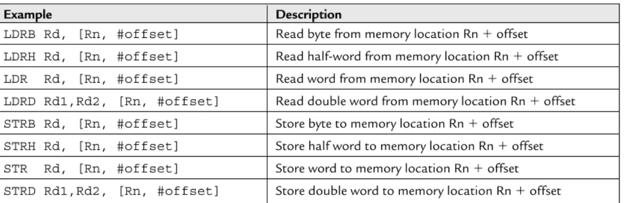
LDRD and STRD ...80
TBB and TBH ...80
Chapter 5 – Memory Systems ... 83
Memory System Features Overview ...83
Memory Maps ...83
Memory Access Attributes ...86
Default Memory Access Permissions ...88
Bit-Band Operations ...88
Advantages of Bit-Band Operations ...92
Bit-Band Operation of Different Data Sizes ...95
Bit-Band Operations in C Programs ...95
Unaligned Transfers ...96
Exclusive Accesses ...98
Endian Mode ...100
Chapter 6 – Cortex-M3 Implementation Overview ... 103
The Pipeline ...103
A Detailed Block Diagram ...105
Bus Interfaces on the Cortex-M3 ...108
The I-Code Bus ...108
The D-Code Bus ...108
The System Bus ...109
The External Private Peripheral Bus ...109
The Debug Access Port Bus ...109
Other Interfaces on the Cortex-M3 ...109
Table of Contents
vii
Prelims-H8534.indd vii
The External Private Peripheral Bus ...109
Typical Connections ...111
Reset Signals ...112
Chapter 7 – Exceptions ... 115
Exception Types ...115
Defi nitions of Priority ...117
Vector Tables ...123
Interrupt Inputs and Pending Behavior...124
Fault Exceptions ...127
Bus Faults...127
Memory Management Faults ...129
Usage Faults ...130
Hard Faults ...132
Dealing with Faults ...132
SVC and PendSV ...133
Chapter 8 – The NVIC and Interrupt Control ... 137
NVIC Overview ...137
The Basic Interrupt Confi guration ...138
Interrupt Enable and Clear Enable ...138
Interrupt Pending and Clear Pending ...138
Priority Levels ...140
Active Status ...141
PRIMASK and FAULTMASK Special Registers ...141
The BASEPRI Special Register ...142
Confi guration Registers for Other Exceptions ...143
Example Procedures of Setting Up an Interrupt ...144
Software Interrupts ...146
The SYSTICK Timer ...147
Chapter 9 – Interrupt Behavior ... 149
Interrupt/Exception Sequences ...149
Stacking ...149
Vector Fetches ...150
Register Updates ...151
Exception Exits ...151
Nested Interrupts ...152
Tail-Chaining Interrupts ...152
Late Arrivals ...153
More on the Exception Return Value ...153
Interrupt Latency ...154
Faults Related to Interrupts ...156
viii
Prelims-H8534.indd viii
Stacking ...156
Unstacking ...157
Vector Fetches ...157
Invalid Returns ...157
Chapter 10 – Cortex-M3 Programming ... 159
Overview ...159
Using Assembly ...159
Using C ...160
The Interface Between Assembly and C ...161
A Typical Development Flow ...162
The First Step ...162
Producing Outputs ...164
The “Hello World” Example ...165
Using Data Memory ...169
Using Exclusive Access for Semaphores ...170
Using Bit Band for Semaphores ...172
Working with Bit Field Extract and Table Branch ...173
Chapter 11 – Exceptions Programming ... 175
Using Interrupts ...175
Stack setup ...175
Vector Table Setup ...176
Interrupt Priority Setup ...177
Enable the Interrupt ...178
Exception/Interrupt Handlers ...179
Software Interrupts ...180
Example with Exception Handlers ...181
Using SVC ...184
SVC Example: Use for Output Functions ...186
Using SVC with C ...189
Chapter 12 – Advanced Programming Features and System Behavior ... 193
Running a System with Two Separate Stacks ...193
Double-Word Stack Alignment ...196
Nonbase Thread Enable ...197
Performance Considerations ...200
Lockup Situations ...201
What Happens During Lockup? ...201
Avoiding Lockup ...202
Chapter 13 – The Memory Protection Unit ... 205
Overview ...205
MPU Registers ...206
Table of Contents
ix
Prelims-H8534.indd ix
Setting Up the MPU ...211
Typical Setup ...217
Example Use of the Subregion Disable ...217
Chapter 14 – Other Cortex-M3 Features ... 223
The SYSTICK Timer ...223
Power Management ...227
Multiprocessor Communication ...229
Self-Reset Control ...231
Chapter 15 – Debug Architecture ... 233
Debugging Features Overview ...233
CoreSight Overview ...234
Processor Debugging Interface ...234
The Debug Host Interface ...235
DP Module, AP Module, and DAP ...235
Trace Interface ...236
CoreSight Characteristics ...237
Debug Modes...239
Debugging Events ...241
Breakpoint in the Cortex-M3 ...243
Accessing Register Content in Debug ...244
Other Core Debugging Features ...245
Chapter 16 – Debugging Components ... 247
Introduction ...247
The Trace System in the Cortex-M3 ...247
Trace Components: Data Watchpoint and Trace ...248
Trace Components: Instrumentation Trace Macrocell ...250
Software Trace with the ITM ...251
Hardware Trace with ITM and DWT ...251
ITM Timestamp ...251
Trace Components: Embedded Trace Macrocell ...252
Trace Components: Trace Port Interface Unit ...253
The Flash Patch and Breakpoint Unit ...253
The AHB Access Port ...256
ROM Table ...257
Chapter 17 – Getting Started with Cortex-M3 Development ... 259
Choosing a Cortex-M3 Product ...259
Differences Between Cortex-M3 Revision 0 and Revision 1 ...260
Revision 1 Change: Moving from JTAG-DP to SWJ-DP ...261
Development Tools ...262
C Compiler ...262
Embedded Operating System Support ...263
x
Prelims-H8534.indd x
Chapter 18 – Porting Applications from the ARM7 to the Cortex-M3 ... 265
Overview ...265
System Characteristics ...266
Memory Map ...266
Interrupts ...266
MPU ...267
System Control ...267
Operation Modes ...267
Assembly Language Files ...268
Thumb State ...268
ARM State ...268
C Program Files ...271
Precompiled Object Files ...271
Optimization ...271
Chapter 19 – Starting Cortex-M3 Development Using the GNU Tool Chain ... 273
Background ...273
Getting the GNU Tool Chain ...273
Development Flow ...274
Examples ...275
Example 1: The First Program ...275
Example 2: Linking Multiple Files ...277
Example 3: A Simple “Hello World” Program ...278
Example 4: Data in RAM ...280
Example 5: C Only, Without Assembly File...281
Example 6: C Only, with Standard C Startup Code ...285
Accessing Special Registers ...287
Using Unsupported Instructions ...287
Inline Assembler in the GNU C Compiler ...287
Chapter 20 – Getting Started with the KEIL RealView
Microcontroller Development Kit ... 289
Overview ...289
Getting Started with Vision ...290
Outputting the “Hello World” Message Via UART ...295
Testing the Software ...298
Using the Debugger ...300
The Instruction Set Simulator ...303
Modifying the Vector Table ...305
Stopwatch Example with Interrupts ...306
Appendix A – Cortex-M3 Instructions Summary ... 315
Supported 16-Bit Thumb Instructions ...315
Supported 32-Bit Thumb-2 Instructions ...319
Table of Contents
xi
Prelims-H8534.indd xi
xii
Appendix B – 16-Bit Thumb Instructions and Architecture Versions ... 329
Appendix C – Cortex-M3 Exceptions Quick Reference ... 331
Exception Types and Enables ...331
Stack Contents After Exception Stacking ...332
Appendix D – NVIC Registers Quick Reference ... 333
Appendix E – Cortex-M3 Troubleshooting Guide ... 347
Overview ...347
Developing Fault Handlers ...348
Report Fault Status Registers ...349
Report Stacked PC ...349
Read Fault Address Register ...350
Clear Fault Status Bits ...350
Others ...350
Understanding the Cause of the Fault ...351
Other Possible Problems ...354
Index ... 355
xii
Prelims-H8534.indd xii
Microcontroller programmers are, by their nature, truly resourceful beings. They take a fi xed design and create fantastic new products by implementing the microcontroller in a very unique way. Constantly, they demand highly effi cient computing from the most frugal of system designs. The primary ingredient used to perform this alchemy is the tool chain environment, and it is for this reason that engineers from ARM’s own tool chain division joined forces with CPU designers to form a team that would rationalize, simplify, and improve upon the ARM7TDMI processor design.
The result of this combination, the ARM Cortex-M3, represents an exciting development to the original ARM architecture. The device blends the best features from the 32-bit ARM architecture with the highly successful Thumb-2 instruction set design whilst adding several new capabilities. Despite these changes, the Cortex-M3 retains a simplifi ed programmer’s model that will be easily recognizable to all existing ARM afi cionados.
—Wayne Lyons
Director of Embedded Solutions, ARM
Foreword
xiii
Prelims-H8534.indd xiii
xiv
This book is for both hardware and software engineers who are interested in the Cortex-M3 processor from ARM. The Cortex-M3 Technical Reference Manual (TRM) and the ARMv7-M Architecture Application Level Reference Manual already provide lots of information on this new processor, but they are very detailed and can be challenging for new starters to read. This book is intended to be a lighter read for programmers, embedded product designers, System-on-a-Chip (SoC) engineers, electronics enthusiasts, academic researchers, and others with some experience of microcontrollers or microprocessors who are investigating the Cortex-M3 processor. The text includes an introduction to the new architecture, an instruction set summary, examples of some instructions, information on hardware features, and an overview of the processor’s advanced debug system. It also provides application examples, including basic steps in software development for the Cortex-M3 processor using ARM tools as well as the GNU tool chain. This book is also targeted to those engineers who are familiar with the ARM7TDMI processor and who are migrating to the Cortex-M3 processor, because it covers the differences between the processors, and the porting of application software from the ARM7TDMI to the Cortex-M3.
Prelims-H8534.indd xiv
xv
Acknowledgments
I would like to thank the following people for reviewing this book or for providing me with their advice and feedback:
Alan Tringham, Dan Brook, David Brash, Haydn Povey, Gary Campbell, Kevin McDermott, Richard Earnshaw, Samin Ishtiaq, Shyam Sadasivan, Simon Axford, Simon Craske, Simon Smith, Stephen Theobald and Wayne Lyons.
I would also like to thank CodeSourcery for their technical support, and Luminary Micro for providing images for the book cover, and of course, the staff at Elsevier for their professional work towards the publication of this book.
Finally, a special thank-you to Peter Cole and Ivan Yardley for inspiring me to write this book.
Prelims-H8534.indd xv
xvi xvi
Abbreviation Meaning
ADK AMBA Design Kit
AHB Advanced High-Performance Bus
AHB-AP AHB Access Port
AMBA Advanced Microcontroller Bus Architecture
APB Advanced Peripheral Bus
ARM ARM ARM Architecture Reference Manual
ASIC Application Specifi c Integrated Circuit
ATB Advanced Trace Bus
BE8 Byte Invariant Big Endian Mode
CPI Cycles Per Instruction
CPU Central Processing Unit
DAP Debug Access Port
DSP Digital Signal Processor/Digital Signal Processing
DWT Data WatchPoint and Trace
ETM Embedded Trace Macrocell
FPB Flash Patch and Breakpoint
FSR Fault Status Register
HTM CoreSight AHB Trace Macrocell
ICE In-Circuit Emulator
IDE Integrated Development Environment
IRQ Interrupt Request (normally refers to external interrupts)
ISA Instruction Set Architecture
ISR Interrupt Service Routine
ITM Instrumentation Trace Macrocell
JTAG Joint Test Action Group (a standard of test/debug interfaces)
JTAG-DP JTAG Debug Port
LR Link Register
LSB Least Signifi cant Bit
LSU Load/Store Unit
MCU Microcontroller Unit
xvi
Prelims-H8534.indd xvi
xvii xvii xvii
MMU Memory Management Unit
MPU Memory Protection Unit
MSB Most Signifi cant Bit
MSP Main Stack Pointer
NMI Nonmaskable Interrupt
NVIC Nested Vectored Interrupt Controller
OS Operating System
PC Program Counter
PSP Process Stack Pointer
PPB Private Peripheral Bus
PSR Program Status Register
SCS System Control Space
SIMD Single Instruction, Multiple Data
SP, MSP, PSP Stack Pointer, Main Stack Pointer, Process Stack Pointer SoC System-on-a-Chip
SP Stack Pointer
SW Serial-Wire
SW-DP Serial-Wire Debug Port
SWJ-DP Serial-Wire JTAG Debug Port
SWV Serial-Wire Viewer (an operation mode of TPIU)
TPA Trace Port Analyzer
TPIU Trace Port Interface Unit
TRM Technical Reference Manual
Terms and Abbreviations
Prelims-H8534.indd xvii
xviii xviii
Various typographical conventions have been used in this book, as follows: • Normal assembly program codes:
MOV R0, R1 ; Move data from Register R1 to Register R0
• Assembly code in generalized syntax; items inside must be replaced by read register names:
MRS <reg>, <special_reg> ; • C program codes:
for (i=0;i<3;i++) { func1(); } • Pseudo code:
if (a > b) { ... • Values:
1. 4'hC , 0x123 are both hexadecimal values
2. #3 indicates item number 3 (e.g., IRQ #3 means IRQ number 3) 3. #immed_12 refers to 12-bit immediate data
4. Register bits
Typically used to illustrate a part of a value based on bit position. For example, bit[15:12] means bit number 15 down to 12.
• Register access types: 1. R is Read only 2. W is Write only
3. R/W is Read or Write accessible
4. R/Wc is Readable and clear by a Write access
Prelims-H8534.indd xviii
xix xix
References
Ref No. Document
1 Cortex-M3 Technical Reference Manual (TRM)
downloadable from the ARM documentation Web site at www.arm.com/documentation/ARMProcessor_Cores/index.html 2 ARMv7-M Architecture Application Level Reference Manual
downloadable from the ARM documentation Web site at www.arm.com/products/CPUs/ARM_Cortex-M3_v7.html 3 CoreSight Technology System Design Guide
downloadable from the ARM documentation Web site at www.arm.com/documentation/Trace_Debug/index.html
4 AMBA Specifi cation
downloadable from the ARM documentation Web site at www.arm.com/products/solutions/AMBA_Spec.html 5 AAPCS Procedure Call Standard for the ARM Architecture
downloadable from the ARM documentation Web site at www.arm.com/pdfs/aapcs.pdf
6 RVCT 3.0 Compiler and Library Guide
downloadable from the ARM documentation Web site at
www.arm.com/pdfs/DUI0205G_rvct_compiler_and_libraries_guide.pdf 7 ARM Application Note 179: Cortex-M3 Embedded Software Development
downloadable from the ARM documentation Web site at www.arm.com/documentation/Application_Notes/index.html
Prelims-H8534.indd xix
1
Introduction
CHAPTER 1
In This Chapter:
● What Is the ARM Cortex-M3 Processor? ● Background of ARM and ARM Architecture ● Instruction Set Development
● The Thumb-2 Instruction Set Architecture (ISA) ● Cortex-M3 Processor Applications
● Organization of This Book ● Further Readings
What Is the ARM Cortex-M3 Processor?
The microcontroller market is vast, with over 20 billion devices per year estimated to be shipped in 2010. A bewildering array of vendors, devices, and architectures are competing in this market. The requirement for higher-performance microcontrollers has been driven globally by the industry’s changing needs; for example, microcontrollers are required to handle more work without increasing a product’s frequency or power. In addition, microcontrollers are becoming increasingly connected, whether by Universal Serial Bus (USB), Ethernet, or Wireless Radio, and hence the processing needed to support these communications channels and advanced peripherals is growing. Similarly, general application complexity is on the increase, driven by more sophisticated user interfaces, multimedia requirements, system speed, and convergence of functionalities. The ARM Cortex-M3 processor, the fi rst of the Cortex generation of processors released by ARM in 2006, was primarily designed to target the 32-bit microcontroller market. The Cortex-M3 processor provides excellent performance at low gate count and comes with many new features previously available only in high-end processors. The Cortex-M3 addresses the requirements for the 32-bit embedded processor market in the following ways:
• Greater performance effi ciency, allowing more work to be done without increasing the frequency or power requirements
CH01-H8534.indd 1
2
• Low power consumption, enabling longer battery life, especially critical in portable products including wireless networking applications
• Enhanced determinism, guaranteeing that critical tasks and interrupts are serviced as quickly as possible but in a known number of cycles
• Improved code density, ensuring that code fi ts in even the smallest memory footprints • Ease of use, providing easier programmability and debugging for the growing number
of 8-bit and 16-bit users migrating to 32-bit
• Lower-cost solutions, reducing 32-bit-based system costs close to those of legacy 8-bit and 16-bit devices and enabling low-end, 32-bit microcontrollers to be priced at less than US$1 for the fi rst time
• Wide choice of development tools, from low-cost or free compilers to full-featured development suites from many development tool vendors
Microcontrollers based on the Cortex-M3 processor already compete head-on with devices based on a wide variety of other architectures. Designers are increasingly looking at reducing the system cost, as opposed to the traditional device cost. As such, organizations are
implementing device aggregation, whereby a single, more powerful device can potentially replace three or four traditional 8-bit devices.
Other cost savings can be achieved by improving the amount of code reuse across all systems. Since Cortex-M3 processor-based microcontrollers can be easily programmed using the C language and are based on a well-established architecture, application code can be ported and reused easily, reducing development time and testing costs.
It is worthwhile highlighting that the Cortex-M3 processor is not the fi rst ARM processor to be used to create generic microcontrollers. The venerable ARM7 processor has been very successful in this market, with partners such as NXP (Philips), Texas Instruments, Atmel, OKI, and many other vendors delivering robust 32-bit Microcontroller Units (MCUs). The ARM7 is the most widely used 32-bit embedded processor in history, with over 1 billion processors produced each year in a huge variety of electronic products, from mobile phones to cars.
The Cortex-M3 processor builds on the success of the ARM7 processor to deliver devices that are signifi cantly easier to program and debug and yet deliver a higher processing capability. Additionally, the Cortex-M3 processor introduces a number of features and technologies that meet the specifi c requirements of the microcontroller applications, such as nonmaskable interrupts for critical tasks, highly deterministic nested vector interrupts, atomic bit manipulation, and an optional memory protection unit. These factors make the Cortex-M3
CH01-H8534.indd 2
Introduction
3
processor attractive to existing ARM processor users as well as many new users considering use of 32-bit MCUs in their products.
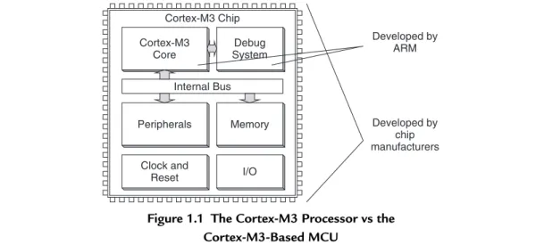
The Cortex-M3 Processor vs Cortex-M3-Based MCUs
The Cortex-M3 processor is the central processing unit (CPU) of a microcontroller chip. In addition, a number of other components are required for the whole M3 processor-based microcontroller. After chip manufacturers license the Cortex-M3 processor, they can put the Cortex-Cortex-M3 processor in their silicon designs, adding memory, peripherals, input/output (I/O), and other features. Cortex-M3 processor-based chips from different manufacturers will have different memory sizes, types, peripherals, and features. This book focuses on the architecture of the processor core. For details about the rest of the chip, please check the particular chip manufacturer’s documentation.
Cortex-M3 Core
Debug System
Memory Peripherals
Internal Bus
Clock and
Reset I/O Cortex-M3 Chip
Developed by ARM
Developed by chip manufacturers
Figure 1.1 The Cortex-M3 Processor vs the Cortex-M3-Based MCU
Background of ARM and ARM Architecture
A Brief History
To help you understand the variations of ARM processors and architecture versions, let’s look at a little bit of ARM history.
ARM was formed in 1990 as Advanced RISC Machines Ltd., a joint venture of Apple Computer, Acorn Computer Group, and VLSI Technology. In 1991, ARM introduced the ARM6 processor family, and VLSI became the initial licensee. Subsequently, additional companies, including Texas Instruments, NEC, Sharp, and ST Microelectronics, licensed the
CH01-H8534.indd 3
4
ARM processor designs, extending the applications of ARM processors into mobile phones, computer hard disks, personal digital assistants (PDAs), home entertainment systems, and many other consumer products.
Nowadays ARM partners ship in excess of 2 billion ARM processors each year. Unlike many semiconductor companies, ARM does not manufacture processors or sell the chips directly. Instead, ARM licenses the processor designs to business partners, including a majority of the world’s leading semiconductor companies. Based on the ARM low-cost and power-effi cient processor designs, these partners create their processors, microcontrollers, and system-on-chip solutions. This business model is commonly called intellectual property (IP) licensing.
In addition to processor designs, ARM also licenses systems-level IP and various software IP. To support these products, ARM has developed a strong base of development tools, hardware, and software products to enable partners to develop their own products.
Architecture Versions
Over the years, ARM has continued to develop new processors and system blocks. These include the popular ARM7TDMI processor and, more recently, the ARM1176TZ(F)-S processor, which is used in high-end applications such as smart phones. The evolution of features and enhancements to the processors over time has led to successive versions of the ARM architecture. Note that architecture version numbers are independent from processor names. For example, the ARM7TDMI processor is based on the ARMv4T architecture (the T is for Thumb instruction mode support).
The ARMv5E architecture was introduced with the ARM9E processor families, including the ARM926E-S and ARM946E-S processors. This architecture added “Enhanced” Digital Signal Processing (DSP) instructions for multimedia applications.
With the arrival of the ARM11 processor family, the architecture was extended to the ARMv6. New features in this architecture included memory system features and Single Instruction– Multiple Data (SIMD) instructions. Processors based on the ARMv6 architecture include the ARM1136J(F)-S, the ARM1156T2(F)-S, and the ARM1176JZ(F)-S.
Following the introduction of the ARM11 family, it was decided that many of the new technologies, such as the optimized Thumb-2 instruction set, were just as applicable to the lower-cost markets of microcontroller and automotive components. It was also decided that although the architecture needed to be consistent from the lowest MCU to the highest-performance application processor, there was a need to deliver processor
architectures that best fi t applications, enabling very deterministic and low gate count processors for cost-sensitive markets and feature-rich and high-performance ones for high-end applications.
CH01-H8534.indd 4
Introduction
5
Over the past several years, ARM extended its product portfolio by diversifying its CPU development, which resulted in the architecture version 7, or v7. In this version, the architecture design is divided into three profi les:
• The A profi le, designed for high-performance open application platforms • The R profi le, designed for high-end embedded systems in which real-time
performance is needed
• The M profi le, designed for deeply embedded microcontroller-type systems Let’s look at these profi les in a bit more detail:
• A Profi le (ARMv7-A): Application processors required to run complex applications such as high-end embedded operating systems (OSs), such as Symbian, Linux, and Windows Embedded, requiring the highest processing power, virtual memory system support with Memory Management Units (MMUs), and, optionally, enhanced Java support and a secure program execution environment. Example products include high-end mobile phones and electronic wallets for fi nancial transactions.
• R Profi le (ARMv7-R): Real-time, high-performance processors targeted primarily at the higher end of the real-time1 market—those applications, such as high-end breaking systems and hard drive controllers, in which high processing power and high reliability are essential and for which low latency is important.
• M Profi le (ARMv7-M): Processors targeting low-cost applications in which
processing effi ciency is important and cost, power consumption, low interrupt latency, and ease of use are critical, as well as industrial control applications, including real-time control systems.
The Cortex processor families are the fi rst products developed on architecture v7, and the Cortex-M3 processor is based on one profi le of the v7 architecture, called ARM v7-M, an architecture specifi cation for microcontroller products.
This book focuses on the Cortex-M3 processor, but it is only one of the Cortex product family that uses the ARMv7 architecture. Other Cortex family processors include the Cortex-A8 (application processor), which is based on the ARMv7-A profi le, and the Cortex-R4 (real-time processor), based on the ARMv7-R profi le.
1 There is always great debate as to whether we can have a “real-time” system using general processors. By
defi nition, “real time” means that the system can get a response within a guaranteed period. In an ARM processor-based system, you may or may not able to get this response due to choice of operating system, interrupt latency, or memory latency, as well as if the CPU is running a higher-priority interrupt.
CH01-H8534.indd 5
6
The details of the ARMv7-M architecture are documented in The ARMv7-M Architecture Application Level Reference Manual (Ref 2). This document can be obtained via the ARM Web site through a simple registration process. The ARMv7-M architecture contains the following key areas:
• Programmer’s model • Instruction set • Memory model • Debug architecture
Processor-specifi c information, such as interface details and timing, is documented in the Cortex-M3 Technical Reference Manual (TRM) (Ref 1). This manual can be accessed freely on the ARM Web site. The Cortex-M3 TRM also covers a number of implementation details not covered by the architecture specifi cations, such as the list of supported instructions, because some of the instructions covered in the ARMv7-M architecture specifi cation are optional on ARMv7-M devices.
Processor Naming
Traditionally, ARM used a numbering scheme to name processors. In the early days (the 1990s), suffi xes were also used to indicate features on the processors. For example, with the ARM7TDMI processor, the T indicates Thumb instruction support, D indicates JTAG debugging, M indicates fast multiplier, and I indicates an embedded ICE module. Subsequently it was decided that these features should become standard features of future ARM processors; therefore, these suffi xes are no longer added to the new processor family
ARM 7TDMI, 920T,
Intel StrongARM Architecture
v4/v4T
Architecture v5/v5E
ARM 926, 946, 966, Intel XScale
Architecture v6
ARM 1136, 1176, 1156T-2
Architecture v7
v7-A (Application; e.g., Cortex-A8)
v7-R (Real-Time; e.g., Cortex-R4)
v7-M (Microcontroller;
e.g., Cortex-M3)
Examples
Figure 1.2 The Evolution of ARM Processor Architecture
CH01-H8534.indd 6
Introduction
7
names. Instead, variations on memory interface, cache, and Tightly Coupled Memory (TCM) have created a new scheme for processor naming.
For example, ARM processors with cache and MMUs are now given the suffi x “26” or “36,” whereas processors with Memory Protection Units (MPUs) are given the suffi x “46” (e.g., ARM946E-S). In addition, other suffi xes are added to indicate synthesizable2 (S) and Jazelle (J ) technology. Table 1.1 presents a summary of processor names.
Processor Name Architecture Version Memory Management Features Other Features
ARM7TDMI ARMv4T ARM7TDMI-S ARMv4T
ARM7EJ-S ARMv5E DSP, Jazelle
ARM920T ARMv4T MMU
ARM922T ARMv4T MMU
ARM926EJ-S ARMv5E MMU DSP, Jazelle
ARM946E-S ARMv5E MPU DSP
ARM966E-S ARMv5E DSP
ARM968E-S ARMv5E DMA, DSP
ARM966HS ARMv5E MPU (optional) DSP
ARM1020E ARMv5E MMU DSP
ARM1022E ARMv5E MMU DSP
ARM1026EJ-S ARMv5E MMU or MPU DSP, Jazelle
ARM1136J(F)-S ARMv6 MMU DSP, Jazelle
ARM1176JZ(F)-S ARMv6 MMU TrustZone DSP, Jazelle
ARM11 MPCore ARMv6 MMU multiprocessor cache support DSP, Jazelle
ARM1156T2(F)-S ARMv6 MPU DSP
Cortex-M3 ARMv7-M MPU (optional) NVIC
Cortex-R4 ARMv7-R MPU DSP
Cortex-R4F ARMv7-R MPU DSP Floating point
Cortex-A8 ARMv7-A MMU TrustZone DSP, Jazelle
Table 1.1 ARM Processor Names
With version 7 of the architecture, ARM has migrated away from these complex numbering schemes that needed to be decoded, moving to a consistent naming for families of processors, with Cortex its initial brand. In addition to illustrating the compatibility across processors, this
2 A synthesizable core design is available in the form of a hardware description language (HDL) such as Verilog
or VHDL and can be converted into a design netlist using synthesis software.
CH01-H8534.indd 7
8
system removes confusion between architectural version and processor family number; for example, the ARM7TDMI is not a v7 processor but was based on the v4T architecture.
Instruction Set Development
Enhancement and extension of instruction sets used by the ARM processors has been one of the key driving forces of the architecture’s evolution.
Historically (since ARM7TDMI), two different instruction sets are supported on the ARM processor: the ARM instructions that are 32-bit and Thumb instructions that are 16-bit. During program execution, the processor can be dynamically switched between the ARM state or the Thumb state to use either one of the instruction sets. The Thumb instruction set provides only a subset of the ARM instructions, but it can provide higher code density. It is useful for products with tight memory requirements.
v4 v4T
ARM
Thumb
v5 v5E v6
Enhanced DSP instructions
added
SIMD, v6 memory
support added
v7
Architecture development Thumb
instructions introduced
Thumb-2 instructions
introduced
Figure 1.3 Instruction Set Enhancement
As the architecture version has been updated, extra instructions have been added to both ARM instructions and the Thumb instructions. Appendix II provides some information on the change of Thumb instructions during the architecture enhancements. In 2003, ARM announced the Thumb-2 instruction set, which is a new superset of Thumb instructions that contains both 16-bit and 32-bit instructions.
The details of the instruction set are provided in a document called The ARM Architecture Reference Manual (also known as the ARM ARM). This manual has been updated for the
CH01-H8534.indd 8
Introduction
9
ARMv5 architecture, the ARMv6 architecture, and the ARMv7 architecture. For the ARMv7 architecture, due to its growth into different profi les, the specifi cation is also split into different documents. For Cortex-M3 developers, the ARM v7-M Architecture Application Level Reference Manual (Ref 2) covers all the required instruction set details.
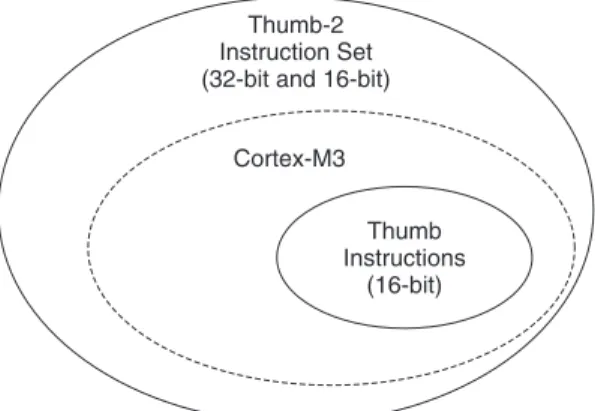
The Thumb-2 Instruction Set Architecture (ISA)
The Thumb-23 ISA is a highly effi cient and powerful instruction set that delivers signifi cant benefi ts in terms of ease of use, code size, and performance. The Thumb-2 instruction set is a superset of the previous 16-bit Thumb instruction set, with additional 16-bit instructions alongside 32-bit instructions. It allows more complex operations to be carried out in the Thumb state, thus allowing higher effi ciency by reducing the number of states switching between ARM state and Thumb state.
Thumb Instructions
(16-bit) Thumb-2 Instruction Set (32-bit and 16-bit)
Cortex-M3
Figure 1.4 The Relationship Between the Thumb-2 Instruction Set and the Thumb
Instruction Set
Focused on small memory system devices such as microcontrollers and reducing the size of the processor, the Cortex-M3 supports only the Thumb-2 (and traditional Thumb) instruction set. Instead of using ARM instructions for some operations, as in traditional ARM processors, it uses the Thumb-2 instruction set for all operations. As a result, the Cortex-M3 processor is not backward compatible with traditional ARM processors. That is, you cannot run a binary image for ARM7 processors on the Cortex-M3 processor. Nevertheless, the Cortex-M3 processor can execute almost all the 16-bit Thumb instructions, including all 16-bit Thumb instructions supported on ARM7 family processors, making application porting easy.
3 Thumb and Thumb-2 are registered trademarks of ARM.
CH01-H8534.indd 9
10
With support for both 16-bit and 32-bit instructions in the Thumb-2 instructions set, there is no need to switch the processor between Thumb state (16-bit instructions) and ARM state (32-bit instructions). For example, in ARM7 or ARM9 family processors, you might need to switch to ARM state if you want to carry out complex calculations or a large number of conditional operations and good performance is needed; whereas in the Cortex-M3 processor, you can mix 32-bit instructions with 16-bit instructions without switching state, getting high code density and high performance with no extra complexity.
The Thumb-2 instruction set is a very important feature of the ARMv7 architecture. Compared with the instructions supported on ARM7 family processors (ARMv4T architecture), the Cortex-M3 processor instruction set has a large number of new features. For the fi rst time, hardware divide instruction is available on an ARM processor, and a number of multiply instructions are also available on the Cortex-M3 processor to improve data-crunching performance. The Cortex-M3 processor also supports unaligned data accesses, a feature previously available only in high-end processors.
Cortex-M3 Processor Applications
With its high performance and high code density and small silicon footprint, the Cortex-M3 processor is ideal for a wide variety of applications:
• Low-cost microcontrollers: The Cortex-M3 processor is ideally suited for low-cost microcontrollers, which are commonly used in consumer products, from toys to electrical appliances. It is a highly competitive market due to the many well-known 8-bit and 16-bit microcontroller products on the market. Its lower power, high performance, and ease-of-use advantages enable embedded developers to migrate to 32-bit systems and develop products with the ARM architecture.
• Automotive: Another ideal application for the Cortex-M3 processor is in the
automotive industry. The Cortex-M3 processor has very high-performance effi ciency and low interrupt latency, allowing it to be used in real-time systems. The Cortex-M3 processor supports up to 240 external vectored interrupts, with a built-in interrupt controller with nested interrupt supports and an optional memory protection unit, making it ideal for highly integrated and cost-sensitive automotive applications. • Data communications: The processor’s low power and high effi ciency, coupled with
Thumb-2 instructions for bit-fi eld manipulation, make the Cortex-M3 ideal for many communications applications, such as Bluetooth and ZigBee.
• Industrial control: In industrial control applications, simplicity, fast response, and reliability are key factors. Again, the Cortex-M3 processor’s interrupt feature, low interrupt latency, and enhanced fault-handling features make it a strong candidate in this area.
CH01-H8534.indd 10
Introduction
11
• Consumer products: In many consumer products, a high-performance microprocessor (or several of them) is used. The Cortex-M3 processor, being a small processor, is highly effi cient and low in power and supports an MPU enabling complex software to execute while providing robust memory protection.
There are already many Cortex-M3 processor-based products available in the market,
including low-end products priced as low as US$1, making the cost of ARM microcontrollers comparable to or lower than that of many 8-bit microcontrollers.
Organization of This Book
This book contains a general overview of the Cortex-M3 processor, with the rest of the contents divided into a number of sections:
Chapters 1 and 2, Introduction and Overview of the Cortex-M3 Chapters 3–6, Cortex-M3 Basics
Chapters 7–9, Exceptions and Interrupts Chapters 10 and 11, Cortex-M3 Programming Chapters 12–14, Cortex-M3 Hardware Features Chapters 15 and 16, Debug Supports in Cortex-M3
Chapters 17–20, Application Development with Cortex-M3 Appendixes
Further Readings
This book does not contain all the technical details on the Cortex-M3 processor. It is intended to be a starter guide for people who are new to the Cortex-M3 processor and a supplemental reference for people using Cortex-M3 processor-based microcontrollers. To get further detail on the Cortex-M3 processor, the following documents, available from ARM (www.arm.com) and ARM partner Web sites, should cover most necessary details:
• The Cortex-M3 Technical Reference Manual (TRM) (Ref 1) provides detailed information about the processor, including programmer’s model, memory map, and instruction timing.
• The ARMv7-M Architecture Application Level Reference Manual (Ref 2) contains detailed information about the instruction set and the memory model.
• Refer to datasheets for the Cortex-M3 processor-based microcontroller products; visit the manufacturer Web site for the datasheets on the Cortex-M3 processor-based product you plan to use.
CH01-H8534.indd 11
12
• Refer to AMBA Specifi cation 2.0 (Ref 4) for more detail regarding internal AMBA interface bus protocol details.
• C programming tips for Cortex-M3 can be found in the ARM Application Note 179: Cortex-M3 Embedded Software Development (Ref 7).
This book assumes that you already have some knowledge of and experience with embedded programming, preferably using ARM processors. If you are a manager or a student who wants to learn the basics without spending too much time reading the whole book or the TRM, Chapter 2 of this book is a good one to read, since it provides a summary on the Cortex-M3 processor.
CH01-H8534.indd 12
13
Overview of the Cortex-M3
CHAPTER 2
In This Chapter: ● Fundamentals ● Registers
● Operation Modes
● The Built-In Nested Vectored Interrupt Controller ● The Memory Map
● The Bus Interface
● The Memory Protection Unit ● The Instruction Set
● Interrupts and Exceptions ● Debugging Support ● Characteristics Summary
Fundamentals
The Cortex-M3 is a 32-bit microprocessor. It has a 32-bit data path, a 32-bit register bank, and 32-bit memory interfaces. The processor has a Harvard architecture, which means it has a separate instruction bus and data bus. This allows instructions and data accesses to take place at the same time, and as a result of this the processor performance increases because data accesses do not affect the instruction pipeline. This feature results in multiple bus interfaces on Cortex-M3, each with optimized usage and the ability to be used simultaneously. However, the instruction and data buses share the same memory space (a unifi ed memory system). In other words, you cannot get 8 GB of memory space just because you have separate bus interfaces. For complex applications that require more memory system features, the Cortex-M3 processor has an optional MPU, and it is possible to use an external cache if it’s required. Both little endian and big endian memory systems are supported.
The Cortex-M3 processor includes a number of fi xed internal debugging components. These components provide debugging operation supports and features such as breakpoints and
CH02-H8534.indd 13
14
watchpoints. In addition, optional components provide debugging features such as instruction trace and various types of debugging interfaces.
Registers
The Cortex-M3 processor has registers R0 to R15. R13 (the stack pointer) is banked, with only one copy of the R13 visible at a time.
R0 to R12: General-Purpose Registers
R0 to R12 are 32-bit general-purpose registers for data operations. Some 16-bit Thumb instructions can only access a subset of these registers (low registers, R0 to R7).
R13: Stack Pointers
The Cortex-M3 contains two stack pointers, R13. They are banked so that only one is visible at a time:
• Main Stack Pointer (MSP): The default stack pointer; used by the OS kernel and exception handlers
• Process Stack Pointer (PSP): Used by user application code Memory Interface
Register Bank
ALU
Instruction Fetch Unit Decoder
Interrupt Controller
(NVIC)
Memory Protection
Unit
Memory System and Peripherals Cortex-M3
Processor Core System
Interrupts
Debug Trace
Instruction Bus Data Bus
Trace Interface
Bus Interconnect
Optional Debug Interface
Debug System
Private Peripherals Code
Memory
Figure 2.1 A Simplifi ed View of the Cortex-M3
CH02-H8534.indd 14
Overview of the Cortex-M3
15
The lowest two bits of the stack pointers are always 0, which means they are always word aligned.
R14: The Link Register
When a subroutine is called, the return address is stored in the link register.
R15: The Program Counter
The program counter is the current program address. This register can be written to control the program fl ow.
Special Registers
The Cortex-M3 processor also has a number of special registers: • Program Status Registers (PSRs)
• Interrupt Mask Registers (PRIMASK, FAULTMASK, BASEPRI) • Control Register (CONTROL)
Name Functions (and Banked Registers)
R0 R1 R2 R3 R4 R5 R6 R7 R8 R9 R10 R11 R12 R13 (MSP)
R14 R15
R13 (PSP)
General-Purpose Register General-Purpose Register General-Purpose Register General-Purpose Register General-Purpose Register General-Purpose Register General-Purpose Register General-Purpose Register General-Purpose Register General-Purpose Register General-Purpose Register General-Purpose Register General-Purpose Register
Main Stack Pointer (MSP), Process Stack Pointer (PSP) Link Register (LR)
Program Counter (PC)
Low Registers
High Registers
Figure 2.2 Registers in the Cortex-M3
CH02-H8534.indd 15
16
These registers have special functions and can be accessed only by special instructions. They cannot be used for normal data processing.
Name
xPSR PRIMASK FAULTMASK
BASEPRI
Functions
Program Status Registers Interrupt Mask
Registers Control Register CONTROL
Special Registers
Figure 2.3 Special Registers in the Cortex-M3
Register Function
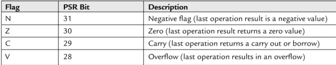
xPSR Provide ALU fl ags (zero fl ag, carry fl ag), execution status, and current executing interrupt number
PRIMASK Disable all interrupts except the nonmaskable interrupt (NMI) and HardFault FAULTMASK Disable all interrupts except the NMI
BASEPRI Disable all interrupts of specifi c priority level or lower priority level CONTROL Defi ne privileged status and stack pointer selection
Table 2.1 Registers and Their Functions
You’ll fi nd more information on these registers in Chapter 3.
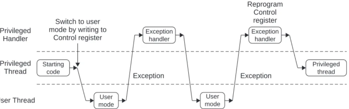
Operation Modes
The Cortex-M3 processor has two modes and two privilege levels. The operation modes (thread mode and handler mode) determine whether the processor is running a normal program or running an exception handler like an interrupt handler or system exception handler. The privilege levels (privileged level and user level) provide a mechanism for safeguarding memory accesses to critical regions as well as providing a basic security model.
Privileged
Handle Mode
Thread Mode Thread Mode
When running an exception
When running main program
Figure 2.4 Operation Modes and Privilege Levels in Cortex-M3
User
CH02-H8534.indd 16
Overview of the Cortex-M3
17
When the processor is running a main program (Thread mode), it can be in either a privileged state or a user state, but exception handlers can only be in a privileged state. When the processor exits reset, it is in Thread mode, with privileged access rights. In the privileged state, a program has access to all memory ranges (except when prohibited by MPU settings) and can use all supported instructions.
Software in the privileged access level can switch the program into the user access level using the control register. When an exception takes place, the processor will always switch back to the privileged state and return to the previous state when exiting the exception handler. A user program cannot change back to the privileged state by writing to the Control register. It has to go through an exception handler that programs the control register to switch the processor back into the privileged access level when returning to Thread mode.
Privileged Handler
User Thread Privileged
Thread Default
Exception Exception
Exit Exception
Exception Exit
Program of Control Register
Figure 2.5 Allowed Operation Mode Transitions
The separation of privilege and user levels improves system reliability by preventing system confi guration registers from being accessed or changed by some untrusted programs. If an MPU is available, it can be used in conjunction with privilege levels to protect critical memory locations such as programs and data for operating systems.
For example, with privileged accesses, usually used by the OS kernel, all memory locations can be accessed (unless prohibited by MPU setup). When the OS launches a user application, it is likely to be executed in the user access level to protect the system from failing due to a crash of untrusted user programs.
The Built-In Nested Vectored Interrupt Controller
The Cortex-M3 processor includes an interrupt controller called the Nested Vectored Interrupt Controller (NVIC). It is closely coupled to the processor core and provides a number of features:
• Nested interrupt support • Vectored interrupt support
CH02-H8534.indd 17
18
• Dynamic priority changes support • Reduction of interrupt latency • Interrupt masking
Nested Interrupt Support
The NVIC provides nested interrupt support. All the external interrupts and most of the system exceptions can be programmed to different priority levels. When an interrupt occurs, the NVIC compares the priority of this interrupt to the current running priority level. If the priority of the new interrupt is higher than the current level, the interrupt handler of the new interrupt will override the current running task.
Vectored Interrupt Support
The Cortex-M3 processor has vectored interrupt support. When an interrupt is accepted, the starting address of the interrupt service routine (ISR) is located from a vector table in memory. There is no need to use software to determine and branch to the starting address of the ISR. Thus it takes less time to process the interrupt request.
Dynamic Priority Changes Support
Priority levels of interrupts can be changed by software during run time. Interrupts that are being serviced are blocked from further activation until the interrupt service routine is completed, so their priority can be changed without risk of accidental reentry.
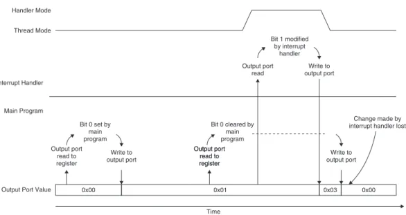
Reduction of Interrupt Latency
The Cortex-M3 processor also includes a number of advanced features to lower the interrupt latency. These include automatic saving and restoring some register contents, reducing delay in switching from one ISR to another (see the discussion of tail chaining interrupts on page 152), and handling late arrival interrupts (see page 153.)
Interrupt Masking
Interrupts and system exceptions can be masked based on their priority level or masked completely using the interrupt masking registers BASEPRI, PRIMASK, and FAULTMASK. They can be used to ensure that time-critical tasks can be fi nished on time without being interrupted.
CH02-H8534.indd 18
Overview of the Cortex-M3
19
The Memory Map
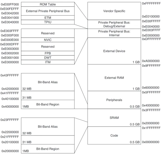
The Cortex-M3 has a predefi ned memory map. This allows the built-in peripherals, such as the interrupt controller and debug components, to be accessed by simple memory access instructions. Thus most system features are accessible in C program code. The predefi ned memory map also allows the Cortex-M3 processor to be highly optimized for speed and ease of integration in system-on-a-chip (SoC) designs.
Overall, the 4 GB memory space can be divided into the ranges shown in Figure 2.6.
Code SRAM External RAM External Device
Peripherals
0x00000000 0x1FFFFFFF 0x20000000 0x3FFFFFFF 0x40000000 0x5FFFFFFF 0x60000000 0x9FFFFFFF
System Level
0xA0000000 0xDFFFFFFF 0xE0000000 0xFFFFFFFF
Mainly used for program code, also provides exception vector table after power-up Mainly used as static RAM Mainly used as peripherals Mainly used as external memory
Mainly used as external peripherals
Private peripherals, including built-in interrupt controller (NVIC), MPU control registers, and debug components
Figure 2.6 The Cortex-M3 Memory Map
The Cortex-M3 design has an internal bus infrastructure optimized for this memory usage. In addition, the design allows these regions to be used differently. For example, data memory can still be put into the CODE region, and program code can be executed from an external RAM region.
The system-level memory region contains the interrupt controller and the debug components. These devices have fi xed addresses, detailed in Chapter 5 (Memory Systems) of this book. By having fi xed addresses for these peripherals, you can port applications between different Cortex-M3 products much more easily.
CH02-H8534.indd 19
20
The Bus Interface
There are several bus interfaces on the Cortex-M3 processor. They allow the Cortex-M3 to carry instruction fetches and data accesses at the same time. The main bus interfaces are:
• Code memory buses • System bus
• Private peripheral bus
The code memory region access is carried out on the code memory buses, which physically consist of two buses, one called I-Code and another called D-Code. These are optimized for instruction fetches for best instruction execution speed.
The system bus is used to access memory and peripherals. This provides access to the SRAM, peripherals, external RAM, external devices, and part of the system-level memory regions. The private peripheral bus provides access to a part of the system-level memory dedicated to private peripherals such as debugging components.
The Memory Protection Unit
The Cortex-M3 has an optional Memory Protection Unit, or MPU. This unit allows access rules to be set up for privileged access and user program access. When an access rule is violated, a fault exception is generated, and the fault exception handler will be able to analyze the problem and correct it if possible.
The MPU can be used in various ways. In common scenarios, the MPU is set up by an operating system, allowing data used by privileged code (e.g., the operating system kernel) to be protected from untrusted user programs. The MPU can also be used to make memory regions read-only, to prevent accidental erasing of data, or to isolate memory regions between different tasks in a multitasking system. Overall, it can help make embedded systems more robust and reliable. The MPU feature is optional and is determined during the implementation stage of the microcontroller or SoC design. For more information on the MPU, refer to Chapter 13.
The Instruction Set
The Cortex-M3 supports the Thumb-2 instruction set. This is one of the most important features of the Cortex-M3 processor because it allows 32-bit instructions and 16-bit instructions to be used together for high code density and high effi ciency. It is fl exible and powerful yet easy to use.
In previous ARM processors, the CPU had two operation states: a 32-bit ARM state and a 16-bit Thumb state. In the ARM state, the instructions are 32-bit and can execute all supported
CH02-H8534.indd 20
Overview of the Cortex-M3
21
instructions with very high performance. In the Thumb state, the instructions are 16-bit, so there is a much higher instruction code density, but the Thumb state does not have all the functionality of ARM instructions and may require more instructions to complete certain types of operations.
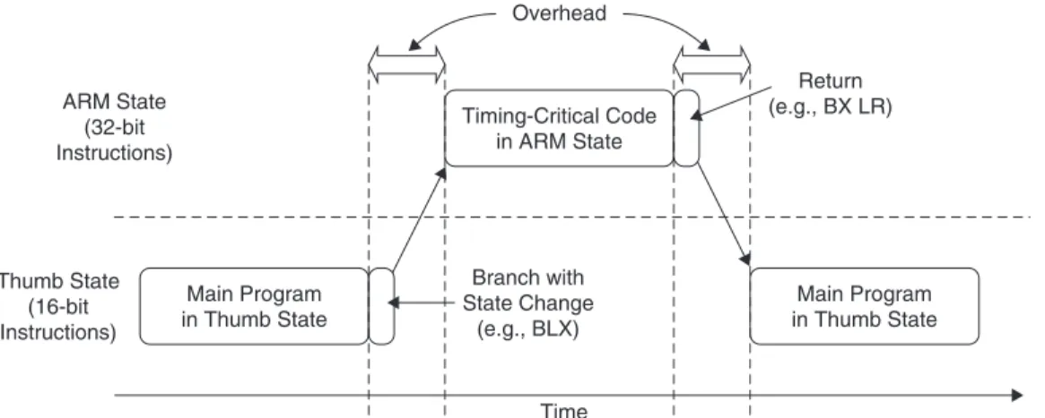
To get the best of both worlds, many applications have mixed ARM and Thumb codes.
However, the mixed-code arrangement does not always work best. There is overhead (in terms of both execution time and instruction space) to switch between the states; and ARM code and Thumb code might need to be compiled separately in different fi les. This increases the complexity of software development and reduces maximum effi ciency of the CPU core.
Timing-Critical Code in ARM State
Main Program in Thumb State
Main Program in Thumb State Thumb State
(16-bit Instructions)
ARM State (32-bit Instructions)
Time Branch with State Change
(e.g., BLX)
Return (e.g., BX LR) Overhead
Figure 2.7 Switching Between ARM Code and Thumb Code in Traditional ARM Processors Such as the ARM7
With the introduction of the Thumb-2 instruction set, it is now possible to handle all processing requirements in one operation state. There is no need to switch between the two. In fact, the Cortex-M3 does not support ARM code. Even interrupts are now handled with the Thumb state. (Previously, the ARM core entered interrupt handlers in the ARM state.) Since there is no need to switch between states, the Cortex-M3 processor has a number of advantages over traditional ARM processors:
• No state switching overhead, saving both execution time and instruction space • No need to separate ARM code and Thumb code source fi les, making software
development and maintenance easier
• It’s easier to get the best effi ciency and performance, in turn making it easier to write software, because there is no need to worry about switching code between ARM and Thumb to try to get the best density/performance
CH02-H8534.indd 21
22
The Cortex-M3 processor has a number of interesting and powerful instructions. Here are a few examples:
• UFBX, BFI, BFC: Bit fi eld extract, insert, and clear instructions • UDIV, SDIV: Unsigned and signed divide instructions
• SEV, WFE, WFI: Send-Event, Wait-For-Event, Wait-For-Interrupts; these allow the processor to handle task synchronization on multiprocessor systems or to enter sleep mode
• MSR, MRS: For access to the special registers
Since the Cortex-M3 processor supports the Thumb-2 instruction set only, existing program code for ARM needs to be ported to the new architecture. Most C applications simply need to be recompiled using new compilers that support the Cortex-M3. Some assembler codes need modifi cation and porting to utilize the new architecture and the new unifi ed assembler framework.
Note that not all the instructions in the Thumb-2 instruction set are implemented on the Cortex-M3. The ARMv7-M Architecture Application Level Reference Manual (Ref 2) only requires a subset of the Thumb-2 instructions to be implemented. For example, coprocessor instructions are not supported on the Cortex-M3 (external data processing engines can be added), and SIMD is not implemented on the Cortex-M3. In addition, a few Thumb instructions are not supported, such as BLX with immediate (used to switch processor state from Thumb to ARM), a couple of CPS instructions, and the SETEND instructions, which were introduced in architecture v6. For a complete list of supported instructions, refer to Appendix A of this book or the Cortex-M3 Technical Reference Manual (Ref 1).
Interrupts and Exceptions
The Cortex-M3 processor implements a new exception model, introduced in the ARMv7-M architecture. This exception model differs from the traditional ARM exception model, enabling very effi cient exception handling. It has a number of system exceptions plus a number of external IRQs (external interrupt inputs). There is no FIQ (fast interrupt in ARM7/9/10/11) in the Cortex-M3; however, interrupt priority handling and nested interrupt support are now included in the interrupt architecture. Therefore, it is easy to set up a system that supports nested interrupts (a higher-priority interrupt can override, or preempt, a lower-priority interrupt handler) and that behaves just like the FIQ in traditional ARM processors.
The interrupt features in the Cortex-M3 are implemented in the NVIC. Aside from supporting external interrupts, the Cortex-M3 also supports a number of internal exception sources, such
CH02-H8534.indd 22
Overview of the Cortex-M3
23
as system fault handling. As a result, the Cortex-M3 has a number of predefi ned exception types, as shown in Table 2.2.
The number of external interrupt inputs is defi ned by chip manufacturers. A maximum of 240 external interrupt inputs can be supported. In addition, the Cortex-M3 also has an NMI interrupt input. When it is asserted, the NMI interrupt service routine is executed unconditionally.
Exception Number Exception Type Priority (Default to 0 Description
if Programmable)
0 NA NA No exception running
1 Reset 3 (Highest) Reset
2 NMI 2 Nonmaskable interrupt
(external NMI input)
3 Hard fault 1 All fault conditions, if the
corresponding fault handler is not enabled
4 MemManage fault Programmable Memory management fault;
MPU violation or access to
illegal locations
5 Bus fault Programmable Bus error (Prefetch Abort or
Data Abort)
6 Usage fault Programmable Exceptions due to program
error
7–10 Reserved NA Reserved
11 SVCall Programmable System service call
12 Debug monitor Programmable Debug monitor (break
points, watchpoints, or external debug request)
13 Reserved NA Reserved
14 PendSV Programmable Pendable request for system
device
15 SYSTICK Programmable System tick timer
16 IRQ #0 Programmable External interrupt #0
17 IRQ #1 Programmable External interrupt #1
… … … …
255 IRQ #239 Programmable External interrupt #239
Table 2.2 Cortex-M3 Exception Types
CH02-H8534.indd 23
24
Debugging Support
The Cortex-M3 processor includes a number of debugging features such as program execution controls, including halting and stepping, instruction breakpoints, data watchpoints, registers and memory accesses, profi ling, and traces.
The debugging hardware of the Cortex-M3 processor is based on the CoreSight architecture. Unlike traditional ARM processors, the CPU core itself does not have a JTAG interface. Instead, a debug interface module is decoupled from the core, and a bus interface called the Debug Access Port (DAP) is provided at the core level. Via this bus interface, external debuggers can access control registers to debug hardware as well as system memory, even when the processor is running. The control of this bus interface is carried out by a Debug Port (DP) device. The DPs currently available are the SWJ-DP (supports the traditional JTAG protocol as well as the Serial Wire protocol) or the SW-DP (supports the Serial Wire protocol only). A JTAG-DP module from the ARM CoreSight product family can also be used. Chip manufacturers can choose to attach one of these DP modules to provide the debug interface. Chip manufacturers can also include an Embedded Trace Macrocell (ETM) to allow
instruction trace. Trace information is output via the Trace Port Interface Unit (TPIU), and the debug host (usually a PC) can then collect the executed instruction information via external trace-capturing hardware.
Within the Cortex-M3 processor, a number of events can be used to trigger debug actions. Debug events can be breakpoints, watchpoints, fault conditions, or external debugging request input signals. When a debug event takes place, the Cortex-M3 can either enter halt mode or execute the debug monitor exception handler.
The data watchpoint function is provided by a Data Watchpoint and Trace (DWT) unit in the Cortex-M3 processor. This can be used to stop the processor (or trigger the debug monitor exception routine) or to generate data trace information. When data trace is used, the traced data can be output via the TPIU. (In the CoreSight architecture, multiple trace devices can share one single trace port.)
In addition to these basic debugging features, the Cortex-M3 processor also provides a Flash Patch and Breakpoint (FPB) unit that can provide a simple breakpoint function or remap an instruction access from Flash to a different location in SRAM.
An Instrumentation Trace Macrocell (ITM) provides a new way for developers to output data to a debugger. By writing data to register memory in the ITM, a debugger can collect the data via a trace interface and display or process it. This method is easy to use and faster than JTAG output. All these debugging components are controlled via the DAP interface bus on the Cortex-M3 or by a program running on the processor core, and all trace information is accessible from the TPIU.
CH02-H8534.indd 24