An Efficient and Analytical Approach for Soft Error Rate Estimation In
Digital Circuits
1Ms. Y. Harika,2Y. Satya Deepthi
1Kakinada Institute of Engineering and Technology for Women, Korangi
2Assistant professor, E.C.E department, Kakinada Institute of Engineering and Technology for Women, Korangi
[email protected],[email protected]
ABSTRACT
Soft errors due to cosmic rays cause reliability problems during lifetime operation of digital systems,
which increase exponentially with Moore’s law. The
first step in developing efficient soft error tolerant schemes is to analyze the effect of soft errors at the system level. This enhanced concept develops a systematic approach for soft error rate estimation. The proposed framework is divided in two stages. First, signal probabilities are computed via a hybrid approach combining heuristics and selective simulation of reconvergent subnets. In the second stage, signal probabilities are used to compute the vulnerability of all the gates in a combinational block using a incremental algorithm Experiments on benchmark circuits and comparison of the results with random fault injection (previous work) show that proposed method is accurate while orders of magnitude faster.
1. INTRODUCTION
Soft errors, also called transient errors, are intermittent malfunctions of the hardware that are not reproducible [1]. Soft errors arise from Single Event Upsets (SEU), which are caused by energetic particles (neutrons and alpha particles). Soft Error Rate (SER) for a device is defined as the error rate due to SEUs, which depends on both the particle flux and circuit characteristics. Device circuit parameters that influence the error rate include the amount of charge stored, the vulnerable cross-sectional area, and the charge collection efficiency. Device scaling significantly affects the susceptibility of integrated circuits to soft errors [2]. As the feature size shrinks, the amount of charge per device decreases enabling a particle strike to be much more likely to cause an error. As a result, particles of lower energy, which are far more plentiful, can generate sufficient charge to cause a soft error. Hence, in the absence of error
correction schemes, the error rate of vulnerable parts will grow in direct proportion to the number of bits on the chip [3]. So far, memory elements have been more susceptible to soft errors than the combinational logic. However, analytical models predict that the soft error rate in the combinational logic will be comparable to that of memory elements by 2011 [2]. Soft error avoidance techniques such as shielding, Silicon-On-Insulator (SOI), and radiation-hardened can only reduce the effect of soft error while introducing significant amount of area and performance penalty. The first step in developing soft error tolerant scheme with low cost and performance penalties is to estimate the system failure rate due to soft errors and the contribution of each component to the overall system failure rate. Previous work on SER estimation is based on fault injection using random simulations and hence inaccurate and very time-consuming [1][2][3].
2. SER ESTIMATION METHODS
estimate SER. In Boolean satisfaction-based approaches, the SER estimation issue is modeled as an equivalent Boolean satisfaction problem, and the exact value of SER can be found by solving that problem. In probability methods, probability of fault propagation toward main outputs and flip-flops is calculated using signals probability and some mathematical equations to model triple masking factors.
Today, reliability estimation plays an important role in the design flow and SER has become one of the most important reliability factors in VLSI circuits. Hence, the SER estimation problem is a significant challenge for circuit designers. During an optimization procedure, a change applies to the circuit to reduce one of the circuit parameters such as power, delay, or SER. Then, the circuit is re-analyzed to determine the improvement in the parameter of interest (here SER) obtained from the applied change.
ANALYTICAL SER ESTIMATION METHOD:
A typical synchronous circuit consists of combinational logic and flip-flops (Fig. 1). Primary Inputs (PIs) and the outputs of flip-flops (PIFF) are inputs of combinational logic (CL). Also, Primary Outputs (POs) and the inputs of the FFs (POFF) are outputs of CL. To compute the error rate of a node in a circuit, three probability factors are required to be computed: ( ) ( ) ( ) SEU i latched i sensitized i R n × P n × P n These parameters are defined as follows:•
RSEU(ni) is the occurrence rate of SEUs at node ni to cause a glitch at the output of the gate. This parameter depends on the energy of the particle, type and the size of the gate, and device characteristics.•
Platched(ni) is the probability that an erroneous value reaching the flip-flop inputs is latched. •
Psensitized(ni) is the probability that node ni is functionally sensitized by the input vectors to propagate the erroneous value from the error site to POs/FFs. RSEU(ni) can be obtained from layout information of library cells, technology parameters, and particle energy [1][4][5]. Platched(ni) estimation consists of logic and timing derating. Logic derating is the probability that an erroneous value is propagated to the input of a flip-flop. Timing derating is the probability that there is an overlap between the width of an error glitch and the latching window of a reachable flip-flop. In this work we focus on the estimation of the logic part of Platched(ni) and Psensitized(ni). This is based on the fact that the error propagation probability computation is the most timeconsuming part of SER estimation. The error
sites considered in this paper are all circuit nodes (inputs and output of all gates and FFs). In the proposed approach, we first extract the structural paths from the error sites to all reachable outputs and then traverse these paths to compute the propagation probability of the erroneous value to the reachable primary outputs or to the reachable flip-flops. Based on the error site, we categorize nets and gates in the circuit as follows. An on-path signal is a net on a path from the error site to a reachable output. Also, an path gate is defined as the gate with at least one on-path input. Finally, an off-on-path signal is a net that is not on-path and is an input of an on-path gate. These three are also shown in Fig. 2. For error propagation probability calculation, as we traverse the paths, we use signal probability for off-path signals and use our propagation rules for on-path signals. The signal probability (SP) of a line l indicates the probability of l having logic value 1 [6]. SP techniques have been presented in [7] [8]. The problem statementcan be described as follows: Given the SEU probability in node ni calculate the probability of the propagation of this error to POs/FFs .
Fig1: typical block diagram of synchronous sequential circuits
(1×0.2=0.2). Similarly, EPP at the output of the gate D (OR gate) is calculated as 0.2×(1-SPB) = 0.2×0.7=0.14. In the general case in which reconvergent paths might exist, the propagation probability from the error site to the output of the reconvergent gate depends on not only the type of the gate and the signal probabilities of the off-path signals, but also the polarities of the propagated error on the on-path signals. To address this issue, we need propagation rules for reconvergent gates. First, we define the Pa(Ui), Pā(Ui), P1(Ui), and P0(Ui) as follow: • Pa(Ui) and Pā(Ui) are defined as the probability of the output of node Ui being a and ā, respectively, whereāis inverted of a. In other words, Pa(Ui) is the probability that the erroneous value is propagated from the error site to Ui with an even number of inversions, whereas Pā(Ui)is the similar propagation probability with an odd number of inversions. • P1(Ui) and P0(Ui) are defined as the probability of the output of node Ui being 1 and 0, respectively. In these cases, the error is blocked and not propagated.Note that Pa(Ui) + Pā(Ui) + P1(Ui) +
P0(Ui) = 1.
MASKING EFFECTS:
Modeling and analyzing the SER in logic is more complex than in memory elements, since there are some well-known masking effects that reduce the overall likelihood that a pulse caused by a particle strike is latched and results in an error. These masking effects are commonly classified as:
Logical masking: Transient faults are masked by gates whose output is independent of the faulty input (e.g., an OR gate with an input set to 1). To model the logical masking, first we need to introduce the concepts of time interval and signal probability: To model the logical masking, first we need to introduce the concepts of time interval and signal probability:
Time interval: In a set of hybrid pulses, each one consists of several single-pulses. If we sort the time of one (zero) to zero (one) transitions of all hybrid pulses in ascending order, the timing distance between two consecutive transitions is called a time interval. It is obvious that the leading and trailing transitions of a time interval do not necessarily have an opposite polarity and both may be from one type; a one (zero) to zero (one) transition. For example, all time intervals related to two single-pulses are shown in Figure 4. Signal probability: signal probability of node k is demonstrated by indicating the probability of that node khas logical value one (‘1’).
Signal probability is considered for those gate inputs on which there is no transient pulse.
Electrical masking: The pulse is attenuated (either its amplitude is reduced or rise/fall times are increased) by the electrical properties of the gates throughout the logic chain, and the resulting magnitude is insufficient to change the value that is latched. As the pulse traverses through the chain of logic gates in the combinational part, it may be attenuated and disappeared due to electrical properties of gates. To model the electrical masking, we use the mathematical equations presented in [10]. In this model, the falling and rising time delays of all gate cells in the library are calculated. Then, the amplitude of the output pulse is computed based on the input pulse width (PWi), the falling and the rising delays of the output pulse.
Timing masking: The pulse arrives at a state-holding element out of its latching-time window. After a transient pulse propagates through the combinational circuit and arrives at a flip-flop, it is stored in the flip-flop and leads to a soft error only if it completely overlaps the latching window of the flip-flop. Otherwise, it is not stored in the flip-flop and a timing masking occurs. The probability that a transient pulse latches at a reachable flip-flop is called Latching Probability (LP). Since the pulse width changes as it is travelling through various gates, after computing the pulse width on the input of a flip-flop, the latching probability is calculated as:
= ( + + )/
INCREMENTAL SOFT ERROR RATE ESIMATION
The circuit delay is one of the most important factors affecting the SER as it plays the key role in the logical, electrical, and time masking mechanisms:
Logical masking: overlapping of two single pulses with the same polarity that has been arrived at separate inputs of a gate will increase the error propagation probability.
Electrical masking: the gate delay has a significant impact on this masking. As the delay of a gate increases, the output pulse attenuation becomes greater.
Time masking: the latching probability of a transient pulse within a flip-flop relates to the time it reaches a flip-flop which is directly related to delay of gates through which the pulse has been traversed.
So, in this section, it is assumed that the changed parameter made by the designer is the gate delay. This change could be the result of changing the gate sizing, the threshold voltage, or other technology parameters. In the following, we introduce a technique to re-estimate the SER resulting from this temporal change. Before describing the proposed algorithm, we explain some concepts.
3. PROPSOED TECHNIQUE
SCAN CHAIN REORDERING
In VLSI design for testability, a scan chain is commonly used to connect the shift registers that store the input and output vectors during the testing phase of manufacturing. Registers in the scan chain are connected as a single path with ends of the path connected to a primary input (PI) pad and a primary output (PO) pad. Test input values are shifted into the registers through the PI pad; then, a test is performed and the test output values are shifted out through the PO pad. Figure 2 depicts a simple example of a scan chain.
Fig 2: scan chain reordering
Also assume that there is a single scan chain in the circuit. As there exists a high correlation between the switching activities in the internal nodes of the circuit with the transitions taking place in the scan cells we further assume that the primary inputs are directly controllable and all the switching activities in the circuit is due to transitions in the scan cells. Our objective is two-fold. They are the following.
(i) To determine the order of interconnection between the scan cells such that the total power consumption due to toggling is minimized.
(ii) To identify the input and output scan cells in the scan chain.
This will reduce the overall average power and also the peak power that may arise while scanning out a captured response. The problem of the capture power (peak power in the test cycle) will be solved by using a novel algorithm that will reorder some cells in the scan chain in such a way that minimizes the Hamming distance between the applied test vector and the captured response in the test cycle, hence reducing the test cycle peak power (capture power). In this scan-chain-ordering algorithm, some cells of the ordered scan chain using the algorithm will be reordered again in order to reduce the peak power which may result during the test cycle.
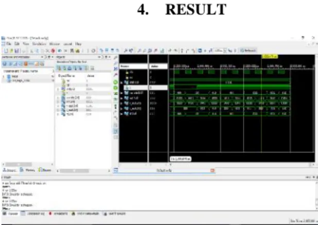
4. RESULT
Fig: Simulation result with error rate
Fig: Simulation result with out error
CONCLUSION
Soft errors due to single event upsets are the main reliability threat of digital systems. In particular, vulnerability of digital systems grows in direct proportion to the Moore's law. In this paper, an accurate propagation probability computation technique has been developed, which significantly reduces the SER estimation time. The proposed approach leverages the signal probability calculation, which is already used in other steps of the design flow, and computes the error propagation probability. Some efficient graph-based algorithms have been used for this computation. To improve the accuracy of our approach, we have considered the output dependencies. Experiments on benchmark circuits and comparison of the results with the random simulation technique show the effectiveness and the accuracy of the presented approach.
REFERENCES:
[1] S. Almukhaizim, Y. Makris, Y. S. Yang, and A.
Veneris, “Seamless Integration of SER in Rewiring
-Based Design Space Exploration,” in Proc.
International Test Conference, 2006, pp. 1–9.
[2] G. Asadi and M. B. Tahoori, “An Accurate SER
Estimation Method Based on Propagation
Proba-bility,” Proc. Design Automation and Test in Europe
Conf, pp. 306–307, 2005
[3] V. Carreno, G. Choi, and R. K. Iyer, “Analog -Digital Simulation of Transient-Induced Logic Er-rors and Upset Susceptibility of an Advanced
Con-trol System,” in NASA Technical Memo 4241, 1990. [4] D. L. Chenette, J. Chen, E. Clayton, T. G. Guzik, J. P. Wefel, M. Garcia-Munoz, C. Lopate, K. R. Pyle,
K. P. Ray, E. G. Mullen, and D. A. Hardy, “The
Environment (CHIME) for Cosmic Ray and Solar Particle Effects on Electronic and Biological Systems
in Space,” IEEE Trans. on Nuclear Science , vol. 41,
no. 6, pp. 2332–2339, 1994.
[5] A. Dharchoudhury, S. M. Kang, H. Cha, and J. H.
Patel, “Fast Timing Simulation of Transient Faults in
Digital Circuits,” in Proc. IEEE/ACM International
Conference on Computer-Aided Design, 1994, pp. 719–722.
[6] P. E. Dodd, F. W. Sexton, G. L. Hash, M. R. Shaneyfelt, B. L. Draper, A. J. Farino, and R. S.
Flores, “Impact of Technology Trends on SEU in CMOS SRAMs,” IEEETrans. Nuclear Science, vol. 43, no. 6, pp. 2797–2804, Dec. 1996.
[7] Graham, “Soft errors a prob- lem as SRAM
geometries shrink,”
http://www.ebnews.com/story/OEG20020128S0079, ebn, 28 Jan 2002.
[8] K. J. Hass and J. W. Ambles, “Single Event Tran
-sients in Deep Submicron CMOS,” 1999.
[9] T. Heijmen and A. Nieuwland, “Soft-Error-Rate Testing of Deep-Submicron Integrated Circuits,” in
Proc. Eleventh IEEE European Test Symposium, 2006, pp. 247–252.
[10] B. Ingols and A. Rambaud, “iRoC Releases Ro
-bust SPARC Test Report,”
http://www.us.designreuse. com/news/news65.html, 2002.
Author’s profile
Ms. Yedla harika Has Completed Her M.Tech (VLSI-SD) from Pragathi Engineering c0llege,JNTUK She is Having 2 Years of Experience In Academics, Currently Working as Assistant Professor at Kakinada Institute Of Engineering and Technology for women