POUR L'OBTENTION DU GRADE DE DOCTEUR ÈS SCIENCES
acceptée sur proposition du jury: Prof. P. Ienne, président du jury
Prof. G. De Micheli, Prof. A. P. Burg, directeurs de thèse Prof. S. Mitra, rapporteur
Prof. E. Macii, rapporteur Prof. J. Sifakis, rapporteur
Verification
THÈSE N
O6863 (2015)
ÉCOLE POLYTECHNIQUE FÉDÉRALE DE LAUSANNE
PRÉSENTÉE LE 18 DÉCEMBRE 2015À LA FACULTÉ INFORMATIQUE ET COMMUNICATIONS LABORATOIRE DES SYSTÈMES INTÉGRÉS (IC/STI)
PROGRAMME DOCTORAL EN INFORMATIQUE ET COMMUNICATIONS
Suisse
PAR
— Winston Churchill
Firstly, I would like to express my sincere gratitude to my advisor Prof. Giovanni De Micheli for giving me the opportunity to pursue my research within the Integrated Systems Laboratory (LSI). His guidance, motivation, and immense knowledge helped me in all time of research. I could not have imagined having a better advisor and mentor for my PhD studies. I am thankful to my co-advisor, Prof. Andreas Burg, for his continuous advices and encouragement throughout the course of my PhD.
Besides my advisors, I would like to thank Dr. Pierre-Emmanuel Gaillardon, who provided me tremendous support and guidance through my doctoral studies. Without his precious help this work would not have been possible.
Furthermore, I am very grateful to Prof. Subhasish Mitra for giving me the opportunity to be a visiting student at Stanford University.
I would like to express my deepest appreciation to Prof. Maciej Ciesielski, Dr. Alan Mishchenko, Prof. Anupam Chattopadhyay, Dr. Robert Wille and Dr. Mathias Soeken for the great research collaborations we had.
My sincere thanks also goes the rest of my thesis committee: Prof. Paolo Ienne, Prof. Joseph Sifakis, Prof. Subhasish Mitra and Prof. Enrico Macii for their their time reading this disserta-tion, their valuable comments and insightful questions.
Tremendous thanks to all my fellow labmates for the stimulating discussions and great mo-ments I had at the LSI laboratory. I want to specially thank Christina Govoni for her kind help and support during my PhD.
Last but not the least, I would like to thank my parents for supporting me throughout my PhD studies and my life in general.
The strong interaction betweenElectronic Design Automation(EDA) tools andComplementary Metal-Oxide Semiconductor(CMOS) technology contributed substantially to the advancement of modern digital electronics. The continuous downscaling of CMOSField Effect Transistor
(FET) dimensions enabled the semiconductor industry to fabricate digital systems with higher circuit density at reduced costs. To keep pace with technology, EDA tools are challenged to handle both digital designs with growing functionality and device models of increasing complexity. Nevertheless, whereas the downscaling of CMOS technology is requiring more complex physical design models, the logic abstraction of a transistor as a switch has not changed even with the introduction of 3D FinFET technology. As a consequence, modern EDA tools are fine tuned for CMOS technology and the underlying design methodologies are based on CMOS logic primitives, i.e., negative unate logic functions. While it is clear that CMOS logic primitives will be the ultimate building blocks for digital systems in the next ten years, no evidence is provided that CMOS logic primitives are also the optimal basis for EDA software. In EDA, the efficiency of methods and tools is measured by different metrics such as (i) the result quality, for example the performance of an automatically synthesized digital circuit, (ii) the runtime and (iii) the memory footprint on the host computer. With the aim to optimize these metrics, the accordance to a specific logic model is no longer important. Indeed, the key to the success of an EDA technique is the expressive power of the logic primitives handling and solving the problem, which determines the capability to reach better metrics.
In this thesis, we investigate new logic primitives for electronic design automation tools. We improve the efficiency of logic representation, manipulation and optimization tasks by taking advantage of majority and biconditional logic primitives. We develop synthesis tools exploiting the majority and biconditional logic expressiveness. Our tools show strong results as compared to state-of-the-art academic and commercial synthesis tools. Indeed, we produce the best (public) results for many circuits in combinational benchmark suites. On top of the enhanced synthesis power, our methods are also the natural and native logic abstraction for circuit design in emerging nanotechnologies, where majority and biconditional logic are the primitive gates for physical implementation.
We accelerate formal methods by (i) studying core properties of logic circuits and (ii) develop-ing new frameworks for logic reasondevelop-ing engines. Thanks to the majority logic representation theory, we prove non-trivial dualities for the property checking problem in logic circuits. Our findings enable sensible speed-ups in solving circuit satisfiability. With the aim of exploiting further the expressive power of majority logic, we develop an alternative Boolean satisfiability
framework based on majority functions. We prove that the general problem is still intractable but we show practical restrictions that instead can be solved efficiently. Finally, we focus on the important field of reversible logic where we propose a new approach to solve the equivalence checking problem. We define a new type of reversible miter over which the equivalence test is performed. Also, we represent the core checking problem in terms of biconditional logic. This enables a much more compact formulation of the problem as compared to the state-of-the-art. Indeed, it translates into more than one order of magnitude speed up for the equivalence checking task, as compared to the state-of-the-art solution.
We argue that new approaches to solve core EDA problems are necessary, as we have reached a point of technology where keeping pace with design goals is tougher than ever.
Key words: Electronic design automation, new logic primitives, logic synthesis, formal meth-ods.
La forte interaction entre les outilsElectronic Design Automation(EDA) et la technologie
Complementary Metal-Oxide Semiconductor(CMOS) a largement contribué à l’avancement de l’électronique numérique moderne. La réduction d’échelle continue des dimensions des trasnsitors permi à l’industrie des semi-conducteurs de fabriquer des systèmes numériques avec une densité de circuit toujours plus élevée à des coûts réduits. Pour suivre le rythme de la technologie, les outils d’EDA sont mis au défi a fin de gérer a la fois la conception du circuits numériques avec de plus en plus avances et des modèles à la complexité croissante. Néanmoins, alors que le réduction d’échelle de la technologie CMOS exige des modèles de conception physiques plus complexes, l’abstraction logique d’un transistor q’un interrup-teur n’a pas changé depuis son origine, même avec l’arrivee de la technologie 3D FinFET. En conséquence, les outils d’EDA modernes sont calibrés pour la technologie CMOS et les méthodologies de conception sous-jacente sont bases sur les primitives logiques du CMOS, à savoir, les fonctions logiques négatives unate. Alors qu’il est clair que les primitives logiques du CMOS resteront les blocs de construction ultimes pour les systèmes numériques dans les dix prochaines années, aucune preuve n’est fournie que CMOS primitives logiques sont egalement la base optimale pour les logiciels d’EDA. Dans EDA, l’efficacité des méthodes et des outils est mesurée par différentes mesures telles que (i) la qualité des résultats, par exemple la performance d’un circuit numérique synthétisé automatiquement, (ii) le temps d’exécution de l’outil et (iii) son empreinte mémoire sur l’ordinateur. Dans le but d’optimiser ces paramètres, l’utilisation d’un modèle logique CMOS n’est plus important. En effet, la clé de la réussite d’une technique EDA est la puissance d’expression des primitives logiques qui permettent la manipulation et la résolution du problème, et celle ci détermine la capacité à atteindre de meilleurs paramètres.
Dans cette thèse, nous étudions de nouvelles primitives logiques pour les outils d’EDA. Nous améliorons l’efficacité des tâches de représentation de la logique, de manipulation et d’optimisation en profitant des operateurs majorité et logiques biconditional. Nous dévelop-pons des techniques et des outils pour la synthèse logique qui exploitent l’expressivité des operations majorité et biconditionales. Nos outils montrent de solides résultats par rapport à l’état-de-l’art universitaires et commerciaux. En effet, nous produisons les meilleurs résultats (publics) pour de nombreux circuits combinatoires. En plus de la puissance de synthèse améliorée, nos méthodes permettent également l’abstraction logique naturelle et native pour la conception de circuits avec du nanotechnologies émergentes, où la majorité et de la logique biconditionele sont des operateurs de base.
Nous accélérons les méthodes de verification formelles par (i) l’étude des propriétés de base de circuits logiques et (ii) le développement de nouveaux principes pour les moteurs de raisonnement logique. Grâce à la théorie supportant la fonction majorité, nous prouvons du dualités non triviales dans des applications de contrôle de propriété pour les circuits logiques. Nos résultats permettent une amélioration de performances dans les probleme des circuit satisfiabilité. Dans le but d’exploiter le pouvoir d’expression de la fonction majorité, nous développons un nouvelle methode permettent de résoudre les problèmes de satisfiabilité. Nous prouvons que le problème général est toujours intraitable mais nous montrons des restrictions pratiques qui peuvent être résolue de manière efficace. Enfin, nous concentrons sur le domaine important de la logique réversible, ou nous avons proposé une nouvelle approche pour résoudre le problème de vérification d’équivalence. Nous définissons une nouvelle formulation reversible sur laquelle la vérification d’équivalence est effectuée. En outre, nous représentons le problème de contrôle de base en termes de logique biconditionelle. Cela permet une formulation beaucoup plus compacte du problème par rapport à l’état-de-l’art. En effet, cela se traduit par plus d’un ordre de grandeur en amélioration de la vitesse pour la tâche de vérification d’équivalence, par rapport à la solution à l’état-de-l’art.
Nous soutenons que de nouvelles approches pour résoudre les principaux problèmes d’EDA sont nécessaires, étant donne que suivre l’evolution de la technologies et des objectifs de conception est plus difficile que jamais.
Mots clefs: Electronic design automation, nouvelles primitives logiques, synthèse logique, méthodes formelles.
La forte interazione tra strumenti per Electronic Design Automation (EDA) e la tecnolo-gia Complementary Metal-Oxide Semiconductor(CMOS) ha contribuito sostanzialmente all’avanzamanto della elettronica digitale moderna. La continua riduzione delle dimensioni dei dispositivi CMOSField Effect Transistor(FET) ha permesso all’industria dei semiconduttori di fabbricare sistemi digitali ad alta densità a costi ridotti. Per tenere il passo con la tecnologia, gli strumenti EDA devono confrontarsi con sistemi digitali sempre più ricchi in funzionalità e modelli fisici sempre più complessi. Anche se la riduzione delle dimensioni dei dispositivi CMOS richiede modelli fisici complessi, l’astrazione logica di un dispositivo CMOS non è cambiata neppure con l’introduzione della tecnologia 3D FinFET. Di conseguenza, gli stru-menti EDA moderni sono altamente perfezionati per la tecnologia CMOS, e le metodologie di progettazione sono basate sulle primitive logiche CMOS, ovvero le funzioni logiche negative unate. Mentre è comunemente accettato che le primitive logiche CMOS saranno i componenti fisici di base per costruire sistemi digitali nei prossimi dieci anni, non è dimostrato che le stesse primitive logiche CMOS sono anche le basi teoriche ottime per i metodi e programmi EDA. Nell’EDA, l’efficienza dei metodi e gli strumenti è misurata da diverse metriche come (i) la qualità dei risultati, per esempio la velocita di un circuito digitale sintetizzato automati-camente, (ii) il tempo di esecuzione e (iii) l’occupazione di memoria in un computer. Con lo scopo di ottimizzare queste metriche, l’accordanza a un modello logico specifico non è importante. Infatti, la chiave del successo per tecniche EDA sta nell’espressività delle primitive logiche con le quali il problema è prima descritto e poi risolto. Questa espressività determina infine la capacità di raggiungere metriche migliori.
In questa tesi studiamo nuove primitive logiche per strumenti EDA.
Miglioriamo l’efficienza della rappresentazione, manipolazione e ottimizzazione logica grazie ai connettivi logici di maggioranza e bicondizionale. Sviluppiamo tecniche e strumenti di sintesi sfruttando l’espressività della logica di maggioranza e bicondizionale. I nostri strumenti mostrano risultati competitivi con strumenti accademici e industriali. Per esempio, produci-amo i migliori risultati pubblici per diversi circuiti in benchmark suites combinatorie. Inoltre alla potenza di sintesi maggiorata, i nostri metodi sono anche la naturale astrazione logica per la progettazione circuitale in nano-tecnologie emergenti, dove la logica di maggioranza e bicondizionale da origine alle porte logiche di base per l’implementazione fisica.
Accelleriamo metodi formali studiando (i) le proprietà logiche dei circuiti e (ii) sviluppando nuove strutture base per motori di ragionamento logico. Grazie alla teoria di rappresentazione logica a maggioranza, proviamo dualità non banali nel controllo di proprietà logiche. Le nostre
scoperte permottono di risolvere più velocemente il problema della soddisfacibilità circuitale. Con lo scopo di sfruttare al meglio l’espressività della logic a maggioranza, sviluppiamo una struttura teorica alternativa, basata sulle funzioni logiche a maggioranza, per approcciare il problema della soddisfacibilità Booleana. Dimostriamo che il problema generale è ancora intrattabile ma proponiamo restrizioni di interesse pratico che invece possono essere risolte efficientemente. Infine, ci concentriamo sul’importante campo della logica reversibile e pro-poniamo un nuovo approccio per risolvere il problema dell’equivalenza formale. Definiamo un nuovo tipo di miter grazie al quale il test di equivalenza è condotto. Inoltre, rappresen-tiamo il problema di equivalenza in termini di logica bicondizionale. Questo permette una formulazione molto più compatta del problema rispetto allo stato dell’arte. Infatti, questo si traduce in un’accellerazione di più di un ordine di grandezza nel verificare l’equivalenza formale rispetto allo stato dell’arte.
Sosteniamo che nuovi approcci per risolvere problemi EDA sono necessari, in quanto abbiamo raggiunto un punto della tecnologia dove tenere il passo con gli obbiettivi di progettazione è più difficile che mai.
Parole chiave: Electronic design automation, nuove primitive logiche, sintesi logica, metodi formali.
Acknowledgements i
Abstract (English/Français/Italiano) iii
List of figures xiii
List of tables xv
1 Introduction 1
1.1 Electronic Design Automation . . . 2
1.2 Modern EDA Tools and Their Logic Primitives . . . 3
1.2.1 Logic Synthesis . . . 4
1.2.2 Formal Methods . . . 4
1.3 Research Motivation . . . 4
1.3.1 Impact on Modern CMOS Technology . . . 5
1.3.2 Impact on Beyond CMOS Technologies . . . 5
1.4 Contributions and Position With Respect to Previous Work . . . 7
1.5 Thesis Organization . . . 9
Part 1: Logic Representation, Manipulation and Optimization 15 2 Biconditional Logic 17 2.1 Introduction . . . 17
2.2 Background and Motivation . . . 19
2.2.1 Binary Decision Diagrams . . . 19
2.2.2 Emerging Technologies . . . 22
2.3 Biconditional Binary Decision Diagrams . . . 23
2.3.1 Biconditional Expansion . . . 24
2.3.2 BBDD Structure and Ordering . . . 24
2.3.3 BBDD Reduction . . . 26
2.3.4 BBDD Complemented Edges . . . 29
2.3.5 BBDD Manipulation . . . 30
2.4 BBDD Representation: Theoretical and Experimental Results . . . 35
2.4.1 Theoretical Results . . . 35
2.5 BBDD-based Synthesis & Verification . . . 40
2.5.1 Logic Synthesis . . . 40
2.5.2 Formal Equivalence Checking . . . 40
2.5.3 Case Study: Design of an Iterative Product Code Decoder . . . 41
2.6 BBDDs as Native Design Abstraction for Nanotechnologies . . . 44
2.6.1 Reversible Logic . . . 45
2.6.2 NEMS . . . 47
2.7 Summary . . . 51
3 Majority Logic 59 3.1 Introduction . . . 59
3.2 Background and Motivation . . . 61
3.2.1 Logic Representation . . . 61
3.2.2 Logic Optimization . . . 62
3.2.3 Notations and Definitions . . . 64
3.3 Majority-Inverter Graphs . . . 66
3.3.1 MIG Logic Representation . . . 66
3.3.2 MIG Boolean Algebra . . . 67
3.3.3 Inserting Safe Errors in MIG . . . 72
3.4 MIG Algebraic Optimization . . . 74
3.4.1 Size-Oriented MIG Algebraic Optimization . . . 74
3.4.2 Depth-Oriented MIG Algebraic Optimization . . . 75
3.4.3 Switching Activity-Oriented MIG Algebraic Optimization . . . 76
3.5 MIG Boolean Optimization . . . 77
3.5.1 Identifying Advantageous Orthogonal Errors in MIGs . . . 77
3.5.2 Depth-Oriented MIG Boolean Optimization . . . 80
3.5.3 Size-Oriented MIG Boolean Optimization . . . 82
3.6 Experimental Results . . . 82
3.6.1 Methodology . . . 82
3.6.2 Optimization Case Study: Adders . . . 84
3.6.3 General Optimization Results . . . 84
3.6.4 ASIC Results . . . 86
3.6.5 FPGA Results . . . 86
3.7 MIGs as Native Design Abstraction for Nanotechnologies . . . 87
3.7.1 MIG-based Synthesis . . . 88
3.7.2 Spin-Wave Devices . . . 88
3.7.3 Resistive RAM . . . 91
3.8 Extension to MAJ-nLogic . . . 95
3.8.1 Generic MAJ-n/INV Axioms . . . 95
3.8.2 Soundness . . . 96
3.8.3 Completeness . . . 98
Part 2: Logic Satisfiability and Equivalence Checking 105
4 Exploiting Logic Properties to Speedup SAT 107
4.1 Introduction . . . 107
4.2 Background and Motivation . . . 109
4.2.1 Notation . . . 109
4.2.2 Tautology Checking . . . 110
4.2.3 Motivation . . . 110
4.3 Properties of Logic Circuits . . . 111
4.4 From Tautology To Contradiction and Back . . . 114
4.4.1 Boolean SAT and Tautology/Contradiction Duality . . . 117
4.5 Experimental Results . . . 118
4.5.1 Verification of SAT Solving Advantage on the Dual Circuit . . . 118
4.5.2 Results for Concurrent Regular/Dual SAT Execution . . . 119
4.6 Summary . . . 120
5 Majority Normal Form Representation and Satisfiability 123 5.1 Introduction . . . 123
5.2 Background and Motivation . . . 124
5.2.1 Notations and Definitions . . . 124
5.2.2 Two-level Logic Representation . . . 124
5.2.3 Satisfiability . . . 125
5.3 Two-Level Majority Representation Form . . . 125
5.3.1 Majority Normal Form Definition and Properties . . . 125
5.3.2 Representation Examples with DNF, CNF and MNF . . . 126
5.4 Majority Satisfiability . . . 128
5.4.1 Complexity of Unrestricted MNF-SAT . . . 128
5.4.2 Complexity of Some Restricted MNF-SAT . . . 128
5.5 Algorithm to Solve MNF-SAT . . . 130
5.5.1 One-level Majority-SAT . . . 130
5.5.2 Decide Strategy for MNF-SAT . . . 132
5.6 Discussion and Future Work . . . 133
5.7 Summary . . . 134
6 Improvements to the Equivalence Checking of Reversible Circuits 137 6.1 Introduction . . . 137
6.2 Background . . . 138
6.2.1 Reversible Circuits . . . 139
6.2.2 Boolean Satisfiability . . . 140
6.3 Mapping Combinational Equivalence Checking for Reversible Circuits to XOR-CNF SAT . . . 141
6.3.1 Creating an Identity Miter . . . 141
6.4 Experimental Results . . . 146
6.4.1 Methodology and Setup . . . 147
6.4.2 Results . . . 148
6.5 Discussion . . . 149
6.5.1 Application to the Verification of Conventional Circuits . . . 149
6.5.2 Easy Exploitation of Parallelism . . . 150
6.6 Summary . . . 150
7 Conclusions 153 7.1 Overview of Thesis Contributions . . . 153
7.2 Open Problems . . . 154
7.3 Concluding Remarks . . . 155
1.1 Design flow. . . 2
1.2 Design verification methods. . . 3
1.3 Common logic abstraction for SiNWFETs, CNFETs, graphene FETs, reversible logic and nanorelays. Logic model: switch driven by a comparator. . . 6
1.4 Common logic abstraction for SWD, RRAM, Graphene reconfigurable gates, QCA and DNA logic. Logic model: majority voter. . . 6
2.1 BDDnon-terminalnode (a) canonical BDD fora·bfunction (b). . . 19
2.2 Common logic abstraction for emerging devices: controllable polarity double-gate FETs in silicon nanowires [12], carbon nanotubes [13], graphene [14] but also six terminal nanorelays [15]. . . 22
2.3 Sketch structure and fabrication images of controllable polarity double-gate SiNWFETs from [12]. . . 23
2.4 BBDDnon-terminalnode. . . 25
2.5 Function to be represented: f =a·b+(a⊕b)·(c¯d),weakROBBDD forf (a) andstrongROBBDD forf (b). . . 27
2.6 Variable swapii+1 involving the CVO levels (PVi+2=w,SVi+2=x), (PVi+1= x,SVi+1=y) and (PVi=y,SVi=z). Effect on nodes at leveli+2 (a)i+1 (b) and i(c). . . 34
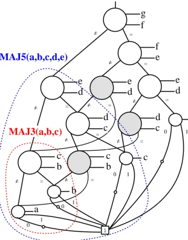
2.7 BBDD for the 7-input majority function. The inclusion of MAJ5and MAJ3 func-tions is illustrated. Grey nodes are nodes with inverted children due tonton−2 majority reduction. . . 36
2.8 Full adder function with BBDDs, variable orderπ=(a,b,ci n). . . 37
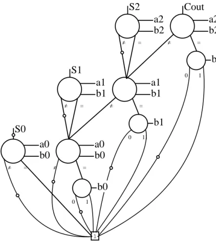
2.9 BBDD for the 3-bit binary adder function, variable orderπ=(a2,b2,a1,b1,a0,b0). 38 2.10 Representations for the bit_comparator circuit in [55] (inverters are bubbles in edges). a) original circuit b) BBDD re-writing, reduced BDD nodes are omitted for the sake of illustration. . . 42
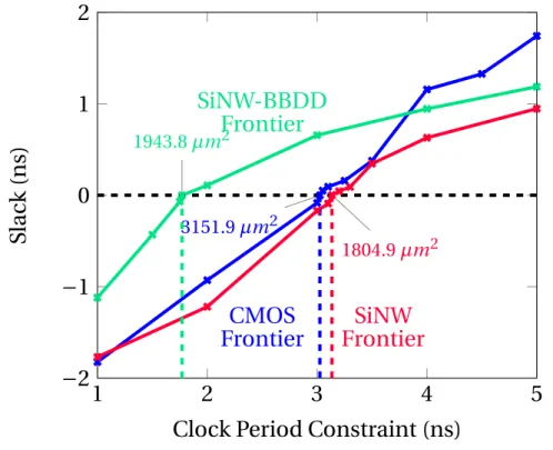
2.11 Targetvs.obtained frequency curves and frequency frontiers for CMOS, SiNW-standard and SiNW-BBDD designs. . . 44
2.12 Reversible circuit made of Toffoli, CNOT and NOT reversible gates. . . 45
2.13 Reversible circuit for a BBDD node [56]. . . 46
2.14 Four-terminals nanorelay structure and fabrication image from [69]. . . 48
2.16 Nanorelay implementation of a full-adder using a BDD-based design approach
[68]. . . 50
2.17 Nanorelay implementation of a full-adder using a BBDD-based design approach. Dotted lines represent6=-edges and solid lines are=-edges. . . 50
3.1 Relations among various functions extracted from [5]. . . 60
3.2 MIG representation forf =x3·(x2+(x01+x0)0). Complementation is represented by bubbles on the edges. . . 67
3.3 Examples of MIG optimization for size, depth and switching activity. . . 75
3.4 Example ofcriticalitycomputation andorthogonalerrors. . . 78
3.5 MIG Boolean depth-optimization example based on critical voters errors inser-tion. Final depth reduction: 60%. . . 80
3.6 Primitive gate areas and designs for SWD technology. All distances are parame-terized with the spin wave wavelengthλSW [56]. . . 89
3.7 Optimization of the MIG representing the functiong=x·(y+u·v). Initial MIG counts 3 nodes and 3 levels. Final MIG counts 3 nodes and 2 levels. . . 90
3.8 SWD circuit implementing functiong, (a) from example in Fig. 3.3(left). (b) from example in Fig. 3.3(right) which is optimized in size and depth. . . 90
3.9 CRS conceptual structure and sweep properties from [70]. . . 92
3.10 Resistive majority operation with BRS/CRS devices [58]. . . 92
3.11 MIG representing the outputpo0in theSencryption operator. . . 94
4.1 Logic circuit example representing the functionf =(ab)d+(ab)c+d c. Thebasis set is {AND, MAJ, INV}. The gates symbolic representation is shown in the box. 109 4.2 AND/OR configuration of a three-input MAJ. . . 111
4.3 Logic circuits examples. {AND, OR, INV} logic circuit representing f =ab+ ac+a(b+c)+a (a). {MAJ, INV} logic circuit emulating the circuit in (a) us-ing constants (b). {AND, OR, INV} logic circuits derived from (a) by switchus-ing AND/OR operators (c). {MAJ, INV} logic circuit emulating the circuit in (a) using an fictitious input variabled(d). . . 112
4.4 Comparison betweenreal invertedandAND/OR switchedlogic circuits repre-senting 4-variable Boolean functions. Theon-setsize ranges from 0 to 24. . . 115
4.5 Speculative parallel regular/dual circuit SAT flow. . . 118
4.6 1000 randomized SAT runs for regular and dual circuit. . . 118
5.1 Two-level representation example for the Boolean functiona+(b·c) in forms: a) DNF, b) CNF, c) MNF and d) more compact MNF. . . 127
6.1 A Toffoli gate. . . 139
6.2 A reversible circuit composed of Toffoli gates . . . 140
6.3 Two functionally equivalent reversible circuits. . . 142
6.4 The resulting identity miter. . . 143
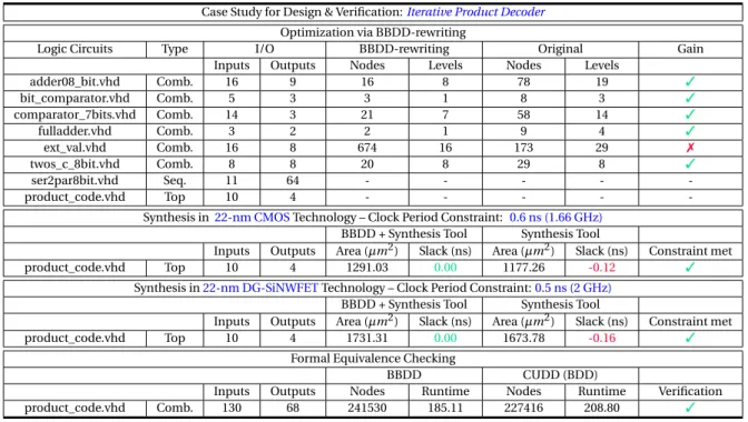
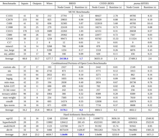
2.1 Experimental results for DD construction using BBDDs, BDDs and KFDDs. . . 39
2.2 Experimental results for BBDD-based Design Synthesis & Verification. . . 43
2.3 Results for reversible circuit synthesis using BBDDs vs. traditional BDDs. . . 47
2.4 Total Number of Relays, the Number of Relays on the Critical Path, and Ratios Compared to [68] (MCNC Benchmark Circuits). . . 49
2.5 Comparison of BDD-based vs. BBDD-based Synthesis of an 8×8 Array Multiplier 51 3.1 Adder Optimization Results . . . 84
3.2 MIG Logic Optimization and LUT-6 Mapping Results . . . 85
3.3 MIG 22-nm ASIC Design Results . . . 86
3.4 MIG 28-nm FPGA Design Results . . . 87
3.5 Cost Functions for MIGs Mapped onto SWDs . . . 89
3.6 Experimental results for SWDs-MIG Synthesis . . . 91
3.7 Summarizing performance results of SWD and CMOS Technologies . . . 91
3.8 Experimental Results for RRAM-MIG Synthesis PRESENT Implementation Per-formances . . . 94
4.1 Switching Rules for Tautology/Contradiction Check . . . 116
4.2 Experimental Results for Regularvs.Dual SAT Solving All runtimes are in seconds119 5.1 Two-Level Logic Representation Comparison. . . 127
The strong interaction betweenElectronic Design Automation(EDA) tools andComplementary Metal-Oxide Semiconductor(CMOS) technology contributed substantially to the advancement of modern digital electronics. The continuous downscaling of CMOSField Effect Transistor
(FET) dimensions enabled the semiconductor industry to fabricate digital systems with higher circuit density and performance at reduced costs [1]. To keep pace with technology, EDA tools are challenged to handle both digital designs with growing functionality and device models of increasing complexity. Nevertheless, whereas the downscaling of CMOS technology is requiring more complex physical design models, the logic abstraction of a transistor as a switch has not changed even with the introduction of 3D FinFET technology [2]. As a consequence, modern EDA tools are fine tuned for CMOS technology and the underlying design methodologies are based on CMOS logic primitives, i.e., negative unate logic functions. While it is clear that CMOS logic primitives will be the ultimate building blocks for digital systems in the next ten years [3], no evidence is provided that CMOS logic primitives are also the optimal basis for EDA software. In EDA, the efficiency of methods and tools is measured by different metrics such as (i) the result quality, for example the performance of an automatically synthesized digital circuit, (ii) the runtime and (iii) the memory footprint on the host computer. With the aim to optimize these metrics, the accordance to a specific logic model is no longer important. Indeed, the key to the success of an EDA technique is the expressive power of the logic primitives handling and solving the problem, which determines the capability to reach better metrics.
Overall, this thesis addresses the general question:“Can EDA logic tools produce better results if based on new, different, logic primitives?”. We show that the answer to this question is affirmative and we give pragmatic examples. We argue that new approaches to solve core EDA problems are necessary, as we have reached a point of technology where keeping pace with design goals is tougher than ever.
1.1 Electronic Design Automation
EDA is an engineering domain consisting of algorithms, methods and tools used to design complex electronic systems. Starting from ahigh-level descriptionof an electronic system, a typical EDA flow operates on several logic abstractions and produces a final implementation in terms of primitive technology components [4]. When targeting anApplication Specific Integrated Circuit(ASIC) technology, the final product is a GDSII file, which represents planar geometric shapes ready for photomask plotting and successive fabrication [5]. When targeting aField-Programmable Gate Arrays(FPGAs) technology, the final product is a binary file, which is used to (re)configure the FPGA device [6].
The main steps involved in the design flow arehigh-level synthesis,logic synthesisandphysical design, also called low level synthesis, which consists ofplacement and routing[4]. They are depicted by Fig. 1.1. High-level synthesisconverts aprogramming language description(or
Figure 1.1: Design flow.
alike) of a logic system into aRegister-Tranfer Level(RTL) netlist.Logic synthesisoptimizes and maps a logic circuit, from an RTL specification, onto standard cells (ASICs) or look-up tables (FPGAs). Placementassigns physical resources to the mapped logic elements, i.e., standard cells inside a chip’s core area (ASICs) or programmable logic blocks (FPGAs).
Routinginterconnects the placed logic elements, i.e., sets wires to properly connect the placed standard cells (ASICs) or creates routing paths between programmable logic elements in a reconfigurable device (FPGAs). All these three steps are subject to area, delay and power minimization metrics. Nowadays, the clear separation between design steps fade away in favor of an integrated approach better dealing with design closure [7]. Contemporary design techniques are fine tuned for CMOS technology. For example, most logic synthesis data structures and algorithms are based on CMOS logic primitives, e.g., negative unate logic functions [4]. Placement and routing algorithms matured with the technological evolution of CMOS down to the nano-scale [3]. Logic or physical characteristics of CMOS technology have
been strong progress drivers for modern design flows.
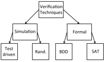
In parallel to the synthesis flow, verification techniques check that the designed system con-forms to specification [8]. Simulationandformal methodsare two popular verification ap-proaches [8]. Simulation techniques compute the output values for given input patterns using simulation models [9]. If the output values mismatch the given specification then verification fails. Simulation-based verification formally succeeds only if the output values match the specification for all input patterns. Because of the exponential space of input patterns, it is im-practical to verify overall designs by simulations. Nevertheless, random simulation techniques are still used as fast bugs hunters. When an exact answer is needed, formal methods precisely prove whether the system conforms to specification or not. In formal methods, specification and design are translated into mathematical models [8]. Formal verification techniques prove correctness with various sorts of mathematical reasoning. It explores all possible cases in the generated mathematical models. Popular mathematical models used in formal methods in-clude mainly Boolean functions/expressions, first order logic, and others. The main reasoning engines used are binary decision diagrams [10] and satisfiability methods [11]. Fig. 1.2 depicts the aforementioned verification environment by means of a diagram.
Verifica(on++
Techniques+
Formal+
Simula(on+
BDD+
SAT+
Rand.+
Test+
driven+
Figure 1.2: Design verification methods.
In this thesis, we focus on thelogic synthesisandformal methodssub-fields of EDA.
1.2 Modern EDA Tools and Their Logic Primitives
Modern EDA tools operate on logic abstractions of an electronic system. These logic asbtrac-tions are based on some primitive logic operators over which the synthesis and verification processes are performed. The expressive power and manipulation properties of the logic primitives employed ultimately determine the quality of the EDA tasks accomplished. We review hereafter the basic logic primitives driving logic synthesis and formal verification tools.
1.2.1 Logic Synthesis
In logic synthesis, the main abstraction is a logic circuit, also called logic network, which is defined over a set of primitive logic gates. Very popular primitive gates in logic synthesis are AND, OR and INV. While there are expensive (in terms of runtime) synthesis techniques operating on truth tables and global functions, most practical synthesis methods exploit the local functionality of primitive gates over which the circuit itself is described. For example, two-level AND-OR logic circuits, also called Sum-Of-Products(SOPs), are synthesized by manipulating cubes and their sum [12]. As cubes are inherently AND functions and their sum is inherently an OR function, two-level logic synthesis is based on AND/OR logic primitives [12]. Another example is about multi-level logic circuits and their synthesis [13]. In multi-level logic representations, logic gates may have an unbounded functionality, meaning that each element can represent an arbitrary logic function. However, these logic elements are often represented internally as SOP polynomials which are factorized into AND/ORs via algebraic methods [13]. Therefore, also multi-level logic synthesis operates on AND/OR logic primitives [13].
1.2.2 Formal Methods
In formal methods, the main logic abstraction is a formal specification. A formal specifi-cation can be a logic circuit, a Boolean formula or any other formal language capable of exhaustively describing the property under test. Ultimately, a formal speficiation is translated into a mathematical logic formula. To prove properties of the formal specification, two core reasoning engines are very popular in formal methods: binary decision diagrams [10] and Boolean satisfiability [11]. Binary decision diagrams are a data structure to represent Boolean functions. They are driven by the Shannon’s expansion to recursively decompose a Boolean function into cofactors until the constant logic values are encountered. Reduced and ordered binary decision diagrams are unique for a given variable order, i.e., canonical. This feature enables efficient property checking. From a logic circuit perspective, the Shannon’s expansion is equivalent to a 2:1 multiplexer (MUX), which therefore is the logic primitive driving binary decision diagrams [10]. Boolean satisfiability consists of determining whether there exists or not an assignment of variables so that a Boolean formula evaluates to true. The standard data structure supporting Boolean satisfiability is theConjunctive Normal Form(CNF), which is a conjunction (AND) of clauses (OR). In other words, this data structure is a two-level OR-AND logic circuits, also called aProduct of Sums(POS). The CNF satisfiability problem is solved through reasoning on clauses (ORs) and how they interact via the top conjunction operator (AND). It follows that standard satisfiability techniques are based on OR/AND logic primitives [11].
1.3 Research Motivation
Nowadays, EDA tools face challenges tougher than ever. On the one hand, design sizes and goals in modern CMOS technology approach the frontier of what is possibly achievable. On
the other hand, post-CMOS technologies bring new computational paradigms for which standard EDA tools are not suitable. New research in fundamental EDA tasks, such as logic synthesis and formal verification, is key to handle this situation.
1.3.1 Impact on Modern CMOS Technology
Present-day EDA tools are based on CMOS logic primitives. For example, AND/OR logic functions, which are the basis for series/parallel gate design rules, drive several synthesis techniques. Similarly, MUX logic functions, which are the primitives for CMOS pass-transistor logic, are the building blocks for canonical data structures. While there is no doubt that these primitives will be the physical building blocks for CMOS digital systems in the next ten years [3], the use of new, more expressive, logic primitives in design and verification methods can improve the computational power of EDA tools.
Indeed, the study of new logic primitives can extend the capabilities of logic synthesis and formal verification tools already in CMOS technology. Exploiting new logic primitives, syn-thesis tools can reach points in the design space not accessible before [14]. Formal methods based on different logic primitives can solve faster an important class of problems, e.g., the verification of arithmetic logic [15], the verification of reversible logic [16], etc.
1.3.2 Impact on Beyond CMOS Technologies
Considering instead post-CMOS technologies, studying new logic primitives is necessary because many emerging nanotechnologies offer an enhanced functionality over standard FET switches [17].
For example, double-gate silicon nanowire FETs [18], carbon nanotube FETs [19], graphene FETs [20, 21] and organic FETs [22] can be engineered to allow device polarity control. The switching function of these devices is biconditional on both gates (polarity and control) values. Four-terminals and six-terminals nanorelays in [23] and [24], respectively, operate similarly. The source to drain connection in these nanorelays is controlled by the gate to body voltage sign and amplitude. In the binary domain, this corresponds to abit comparatorbetween the gate and body logic values. Also reversible logic gates, such as Toffoli gates, embed the biconditional connective in their operation [25]. Indeed, biconditional (XNOR) operations are easily reversible while other logic operations, such as conjunctions and disjunctions, are not. All these devices operate as a switch driven by asingle bit comparator. Fig. 1.3 depicts the common logic abstraction for those comparator-intrinsic nanodevices.
Other promising nanodevices, such as Spin-Wave Devices (SWD) [26–28], Resistive RAM
(RRAM) [29, 30] and graphene reconfigurable gates [31], operate using different physical phenomena than standard FETs. For example, SWD uses spin waves as information carrier while CRS logic behavior depends on the previous memory state. In those nanotechnolo-gies, the circuit primitive is not anymore a standard switch but a three-input majority voter.
A B CNFETs
SiNWFETs
Graphene FETs Reversible Logic
6T Nanorelays 4T Nanorelays t" c2" (c1"c2"…"cn)""""t"⊕ c1" cn" c2" c1" cn"
Figure 1.3: Common logic abstraction for SiNWFETs, CNFETs, graphene FETs, reversible logic and nanorelays. Logic model: switch driven by a comparator.
Note that there are other nanotechnologies where majority voters are the circuit primitive. Quantum-dot cellular automata is one well-known voting-intrinsic nanotechnology [32]. Also, DNA strand displacement recently showed the capability to implement voting logic [33]. Fig. 1.4 depicts the common logic abstraction for these voting-intrinsic nanodevices.
RRAM Spin-Wave Device DNA Logic QCA Graphene RG MAJ$ z$ y$ x$
f
!
$
Figure 1.4: Common logic abstraction for SWD, RRAM, Graphene reconfigurable gates, QCA and DNA logic. Logic model: majority voter.
essential to permit a fair evaluation on nanotechnologies with logic abstractions different than standard CMOS [34].
1.4 Contributions and Position With Respect to Previous Work
This thesis is centered around logic synthesis and formal methods. For the sake of complete-ness, we also include our results in the area of nanotechnology design. Our contributions can be classified into two main categories.
1) Logic Representation, Manipulation and Optimization
Contributions
We develop new compact representations for logic functions, together with powerful manip-ulation and optimization techniques. The two main topics here arebiconditional logicand
majority logic.
Position With Respect to Previous Work
Regardinglogic representation, manipulation and optimization, state-of-the-art design tools make extensive use of homogeneous logic networks. Homogeneous logic networks are directed acyclic graphs where all internal nodes represent the same logic function and edges are possibly complemented in order to preserve universality. And-Inverter Graphs(AIGs) are homogeneous logic networks driven by the AND logic function [35]. AIGs are widely used in logic optimization. AIG optimization algorithms are typically based on fast and local rewriting rules, together with traditional Boolean techniques [35–37].Binary Decision Diagrams(BDDs) are homogeneous logic networks driven by the MUX logic function [10]. With specific ordering and reduction rules, BDDs are canonical, i.e., unique for a logic function and variable order [10]. BDDs are commonly employed both as a representation structure and as a logic manipulation engine for optimization. Indeed, the canonicity of BDDs enables efficient computation of cofactors, Boolean difference and approximation ofdon’t caresets, all important features to logic optimization techniques [38, 39].
Our contributions in this category focus on homogeneous logic networks as well. We propose
Majority-Inverter Graphs(MIGs), an homogeneous logic network driven by ternary majority logic functions. As majority functions can be configured to behave as AND/ORs, MIGs can be more compact than AIGs. Moreover, MIG manipulation is supported by a sound and complete algebraic framework and unique Boolean properties. Such features makes MIG optimization extremely effective as compared to the state-of-the-art counterparts. We propose
Biconditional Binary Decision Diagrams(BBDDs), a BDD-like homogeneous logic network where branching decisions are biconditional on two variables per time rather than on only one. From a theoretical perspective, considering two variables per time enhances the expressive
power of a decision diagram. Nevertheless, BBDDs are still canonical with respect to specific ordering and reduction rules. BBDDs improve the efficiency of traditional EDA tasks based on decision diagrams, especially for arithmetic intensive designs. Indeed, BBDDs are smaller than BDDs for notable arithmetic functions, such as binary addition and majority voting. On the other hand, BBDDs represent the natural and native design abstraction for emerging technologies where the circuit primitive is a comparator, rather than a simple switch. 2) Boolean Satisfiability and Equivalence Checking
Contributions
We study logic transformations to speed up satisfiability check in logic circuits. We develop an alternative Boolean satisfiability framework based on majority logic rather than standard conjunctive normal form. Finally, we propose a new approach to solve sensibly faster the combinational equivalence checking problem for reversible logic.
Position With Respect to Previous Work
For the BooleanSATisfiability(SAT) problem, the state-of-the-art solution use aConjunctive Normal Form(CNF) formulation solved by modern variants of theDavis Putnam Logemann Loveland(DPLL) algorithm, such as conflict-driven clause learning [11]. For the Combina-tional Equivalence Checking(CEC) problem, the state-of-the-art solution first creates a miter circuit by XOR-ing bit-wise the outputs of the two circuits under test. Then, it uses simulation and BDD/SAT sweeping on the input side (i.e., proving equivalence of some internal nodes in a topological order), interleaved with attempts to run SAT on the outputs (i.e., proving equivalence of all the outputs to constant 0) [40].
Our contributions in this category focus on alternative SAT formulations and CEC solving approaches. We define aMajority Normal Form(MNF), a two-level logic representation form based on genericn-ary majority operators. When described over a MNF, the SAT problem has remarkable properties. For example, practical restrictions of the MNF-SAT problem can be solved in polynomial time. Considering instead circuit satisfiability, we discover circuit dualities useful to speed-up SAT solving via parallel execution. Moving to CEC, we focus on the problem of checking the equivalence of reversible circuits. Here, the state-of-the art CEC solution is still the standardmiter-sweeping-SATone. We propose a different type of miter, obtained by cascading the two reversible circuits under test in place of XOR-ing them. As a result, we do not aim at proving the unSAT of the outputs anymore, but we aim at proving that the outputs all represent the identity function. In this scenario, we propose an efficient XOR-CNF formulation of the identity check problem which is solvable via Gaussian elimination and SAT. Such reversible CEC flow decreases the runtime by more than one order of magnitude as compared to state-of-the-art solutions.
In both categories 1) and 2), our research contributions exploit new logic primitives to ap-proach fundamental EDA problems from a different, unconventional, perspective.
1.5 Thesis Organization
This thesis is divided into two parts:Logic Representation, Manipulation and Optimization
andBoolean Satisfiability and Equivalence Checking. For the sake of clarity and readability, each chapter comes with separate background, notations and bibliography sections.
Part 1 Logic Representation, Manipulation and Optimization.Chapters 2-3.
Chapter 2presents Biconditional Binary Decision Diagrams(BBDDs), a novel canonical representation form for Boolean functions. BBDDs are binary decision diagrams where the branching condition, and its associated logic expansion, is biconditional on two variables. Empowered by reduction and ordering rules, BBDDs are remarkably compact and unique for a Boolean function. BBDDs improve the efficiency of traditional EDA tasks based on decision diagrams, especially for arithmetic intensive designs. BBDDs also represent the natural and native design abstraction for emerging technologies where the circuit primitive is a comparator, rather than a simple switch. Thanks to an efficient BBDD software package implementation, we validate 1) speed-up in traditional decision diagrams and 2) improved synthesis of circuits in traditional and emerging technologies.
Chapter 3proposes a paradigm shift in representing and optimizing logic by using only majority (MAJ) and inversion (INV) functions as basic operations. We represent logic functions byMajority-Inverter Graph(MIG): a directed acyclic graph consisting of three-input majority nodes and regular/complemented edges. We optimize MIGs via a new Boolean algebra, based exclusively on majority and inversion operations, that we formally axiomatize in this thesis. As a complement to MIG algebraic optimization, we develop powerful Boolean methods exploiting global properties of MIGs, such as bit-error masking. MIG algebraic and Boolean methods together attain very high optimization quality. Furthermore, MIG optimization improves the synthesis of emerging nanotechnologies whose logic primitive is a majority voter.
Part 2 Boolean Satisfiability and Equivalence Checking.Chapters 4-6.
Chapter 4establishes a non-trivial duality between tautology and contradiction check to speed up circuit satisfiability (SAT). Tautology check determines if a logic circuit is true in every possible interpretation. Analogously, contradiction check determines if a logic circuit is false in every possible interpretation. A trivial transformation of a (tautology, contradiction) check problem into a (contradiction, tautology) check problem is the inversion of all outputs in a logic circuit. In this work, we show that exact logic inversion is not necessary. We give operator switching rules that selectively exchange tautologies with contradictions, and viceversa. Our approach collapses into logic inversion just for tautology and contradiction extreme points
but generates non-complementary logic circuits in the other cases. This property enables solving speed-ups when an alternative, but equisolvable, instance of a problem is easier to solve than the original one. As a case study, we investigate the impact on SAT. We show a 25% speed-up of SAT in a concurrent execution scenario.
Chapter 5introduces an alternative two-level logic representation form based solely on major-ity and complementation operators. We call itMajority Normal Form(MNF). MNF is universal and potentially more compact than its CNF and DNF counterparts. Indeed, MNF includes both CNF and DNF representations. We study the problem of MNF-SATisfiability (MNF-SAT) and we prove that it belongs to the NP-complete complexity class, as its CNF-SAT counterpart. However, we show practical restrictions on MNF formula whose satisfiability can be decided in polynomial time. We finally propose a simple core procedure to solve MNF-SAT, based on the intrinsic functionality of two-level majority logic.
Chapter 6presents a new approach for checking the combinational equivalence of two re-versible circuit significantly faster than the state-of-the-art. We exploit inherent characteristics of reversible computation, namely bi-directional (invertible) execution and the XOR-richness of reversible circuits. Bi-directional execution allows us to create an identity miter out of two reversible circuits to be verified, which naturally encodes the equivalence checking problem in the reversible domain. Then, the abundant presence of XOR operations in the identity miter enables an efficient problem mapping into XOR-CNF satisfiability. The resulting XOR-CNF formulas are eventually more compact than pure CNF formulas and potentially easier to solve. Experimental results show that our equivalence checking methodology is more than one order of magnitude faster, on average, than the state-of-the-art solution based on established CNF-formulation and standard SAT solvers.
Chapter 7concludes the thesis. A summary of research accomplishments is presented, which affirmatively answers the question:“Can EDA logic tools produce better results if based on new, different, logic primitives?”. Possible future works are finally discussed.
[1] G. E. Moore,Cramming more components onto integrated circuits, Proceedings of the IEEE 86.1 (1998): 82-85.
[2] D. Hisamoto, et al.,FinFET-a self-aligned double-gate MOSFET scalable to 20 nm, IEEE Transactions on Electron Devices 47.12 (2000): 2320-2325.
[3] M. Bohr,Technology Insight: 14 nm Process Technology - Opening New Horizons, Intel Developer Forum 2014 - San Francisco.
[4] G. De Micheli,Synthesis and optimization of digital circuits, McGraw-Hill Higher Educa-tion, 1994.
[5] J. Buchanan,The GDSII Stream Format, June 1996.
[6] S. Brown, et al.Field-programmable gate arrays. Vol. 180. Springer Science & Business Media, 2012.
[7] A. Kahng, et al.VLSI physical design: from graph partitioning to timing closure, Springer Science & Business Media, 2011.
[8] E. Clarke, J. M. Wing.Formal methods: State of the art and future directionsACM Comput-ing Surveys (CSUR) 28.4 (1996): 626-643.
[9] F. Krohm,The use of random simulation in formal verificationIEEE International Confer-ence on Computer Design, 1996.
[10] R.E. Bryant,Graph-based algorithms for Boolean function manipulation, IEEE Trans. on Comp., C-35(8): 677-691, 1986.
[11] A. Biere, et al. eds.Handbook of satisfiability, Vol. 185. ios press, 2009.
[12] R.L. Rudell, A. Sangiovanni-Vincentelli,Multiple-valued minimization for PLA optimiza-tion, IEEE Trans. CAD, 6(5): 727-750, 1987.
[13] R. K. Brayton, G. D. Hachtel, A. L. Sangiovanni-Vincentelli, Multilevel logic synthesis, Proceedings of the IEEE 78.2 (1990): 264-300.
[14] L. Amaru, P.-E. Gaillardon, G. De Micheli,Majority-Inverter Graph: A Novel Data-Structure and Algorithms for Efficient Logic Optimization,Design Automation Conference (DAC), San Francisco, CA, USA, 2014.
[15] M. Ciesielski, C. Yu, W. Brown, D. Liu, A. Rossi,Verification of Gate-level Arithmetic Circuits by Function ExtractionIn ACM Design Automation Conference (DAC-2015). 2015. [16] L. Amaru, P.-E. Gaillardon, R. Wille, G. De Micheli,Exploiting Inherent Characteristics of
Reversible Circuits for Faster Combinational Equivalence Checking, DATE’16.
[17] K. Bernsteinet al.,Device and Architecture Outlook for Beyond CMOS Switches, Proceed-ings of the IEEE, 98(12): 2169-2184, 2010.
[18] T. Ernst,Controlling the Polarity of Silicon Nanowire Transistors, Science 340, 1414 (2013); [19] Y.-M, Lin,et al.,High-performance carbon nanotube field-effect transistor with tunable
polarities, Nanotechnology, IEEE Transactions on 4.5 (2005): 481-489.
[20] Heejun Yanget al.,Graphene Barristor, a Triode Device with a Gate-Controlled Schottky Barrier, Science 336, 1140 (2012).
[21] S.-L. Li, et al., Complementary-Like Graphene Logic Gates Controlled by Electrostatic Doping, Small 7.11 (2011): 1552-1556.
[22] S. Iba,et al.,Control of threshold voltage of organic field-effect transistors with double-gate structures, Applied Physics Letters 87.2 (2005): 023509.
[23] D. Lee,et al. Combinational logic design using six-terminal NEM relays, Computer-Aided Design of Integrated Circuits and Systems, IEEE Transactions on 32.5 (2013): 653-666. [24] M. Spencer, et al.,Demonstration of integrated micro-electro-mechanical relay circuits for
VLSI applications, IEEE Journal of Solid-State Circuits, 46.1: 308-320, 2011.
[25] T. Toffoli, Reversible computing, in Automata, Languages and Programming, W. de Bakker and J. van Leeuwen, Eds. Springer, 1980, p. 632, technical Memo MIT/LCS/TM-151, MIT Lab. for Comput. Sci.
[26] T. Schneider,et al.,Realization of spin-wave logic gates, Applied Physics Letters 92.2 (2008): 022505.
[27] Khitun, Alexander, and Kang L. Wang. "Nano scale computational architectures with Spin Wave Bus." Superlattices and Microstructures 38.3 (2005): 184-200.
[28] A. Khitun, et al., Non-volatile magnonic logic circuits engineering, Journal of Applied Physics, 110:034306, Aug. 2011.
[29] E. Linn, R. Rosezin, C. Kügeler, R. Waser, "Complementary resistive switches for passive nanocrossbar memories,"Nature Materials, 9, 2010.
[30] E. Linn, R. Rosezin, S. Tappertzhofen, U. Böttger, R. Waser, "Beyond von Neumann–logic operations in passive crossbar arrays alongside memory operations,"Nanotechnology, 23(305205), 2012.
[31] Sandeep Miryala et al.,Exploiting the Expressive Power of Graphene Reconfigurable Gates via Post-Synthesis Optimization, Proc. GLVSLI’15.
[32] I. Amlani, et al.Digital logic gate using quantum-dot cellular automata, Science 284.5412 (1999): 289-291.
[33] Li, Wei, et al. "Three-input majority logic gate and multiple input logic circuit based on DNA strand displacement." Nano letters 13.6 (2013): 2980-2988.
[34] L. Amaru, P.-E. Gaillardon, S. Mitra, G. De Micheli,New Logic Synthesis as Nanotechnology Enabler, accepted in Proceedings of the IEEE, 2015.
[35] A. Mishchenko, S. Chatterjee, R. K. Brayton,DAG-aware AIG rewriting a fresh look at combinational logic synthesis, In Proceedings of the 43rd annual Design Automation Conference (pp. 532-535), 2006.
[36] A. Mishchenko, et al.Delay optimization using SOP balancing, Proc. ICCAD, 2011. [37] A. Mishchenkoat al., Using simulation and satisfiability to compute flexibilities in Boolean
networks, IEEE TCAD 25 (5): 743-755, 2006.
[38] O. Coudert, J.C. Madre,A unified framework for the formal verification of sequential circuits, Proc. ICCAD, 1990
[39] O. Coudert, C. Berthet, J.C. Madre,Verification of sequential machines using boolean functional vectors, Proc. International Workshop on Ap- plied Formal Methods for Correct VLSI Design, 1989.
[40] A. Mishchenko, et al.Improvements to combinational equivalence checking, IEEE/ACM International Conference on. Computer-Aided Design, 2006. ICCAD’06.
lation and Optimization
The first part of this thesis is dedicated to logic representation, manipulation and optimization. It deals with two main topics: biconditional logic and majority logic. For biconditional logic, a new canonical binary decision diagram is introduced, examining two variables per decision node rather than only one. For majority logic, a directed-acyclic graph consisting of three-input majority nodes and regular/complemented edges is presented, together with a native Boolean algebra.
In this chapter, we presentBiconditional Binary Decision Diagrams(BBDDs), a novel canonical representation form for Boolean functions. BBDDs are binary decision diagrams where the branching condition, and its associated logic expansion, is biconditional on two variables. Empowered by reduction and ordering rules, BBDDs are remarkably compact and unique for a Boolean function. The interest of such representation form in modernElectronic Design Automation(EDA) is twofold. On the one hand, BBDDs improve the efficiency of traditional EDA tasks based on decision diagrams, especially for arithmetic intensive designs. On the other hand, BBDDs represent the natural and native design abstraction for emerging technologies where the circuit primitive is a comparator, rather than a simple switch. We provide, in this chapter, a solid ground for BBDDs by studying their underlying theory and manipulation properties. Thanks to an efficient BBDD software package implementation, we validate (i) runtime reduction in traditional decision diagrams applications with respect to other DDs, and (ii) improved synthesis of circuits in standard and emerging technologies.
2.1 Introduction
The choice of data structure is crucial in computing applications, especially for the automated design of digital circuits. When logic functions are concerned,Binary Decision Diagrams
(BDDs) [1–3] are a well established cogent and unique, i.e., canonical, logic representation form. BDDs are widely used inElectronic Design Automation(EDA) to accomplish important tasks, e.g., synthesis [4], verification [5], testing [6], simulation [7], and others. Valuable ex-tensions [8] and generalizations [9] of BDDs have been proposed in literature to improve the performance of EDA applications based on decision diagrams. The corresponding software packages [10, 11] are indeed mature and supported by a solid theory. However, there are still combinational designs, such as multipliers and arithmetic circuits, that do not fit modern computational capabilities when represented by existing canonical decision diagrams [24]. The quest for new data structures handling such hard circuits, and possibly pushing further the performance for ordinary circuits, is of paramount importance for next-generation dig-ital designs. Furthermore, the rise of emerging technologies carrying new logic primitives
demands for novel logic representation forms that fully exploit a diverse logic expressive power. For instance, controllable polarityDouble-Gate(DG) transistors, fabricated in silicon nanowires [12], carbon nanotubes [13] or graphene [14] technologies, but also nanorelays [15], intrinsically behave as comparators rather than switches. Hence, conventional data structures are not appropriate to model natively their functionality [16].
In this chapter, we presentBiconditional Binary Decision Diagrams(BBDDs), a novel canonical BDD extension. While original BDDs are based on the single-variable Shannon’s expansion, BBDDs employ a two-variable biconditional expansion, making the branching condition at each decision node dependent on two variables per time. Such feature improves the logic expressive power of the binary decision diagram. Moreover, BBDDs represent also the natural and native design abstraction for emerging technologies [12–15] where the circuit primitive is a comparator, rather than a switch.
We validate the benefits deriving from the use of BBDDs in EDA tasks through an efficient software manipulation package, available online [19]. Considering the MCNC benchmark suite, BBDDs are built 1.4×and 1.5×faster than original BDDs andKronecker Functional Decision Diagrams(KFDDs) [9], while having also 1.5×and 1.1×fewer nodes, respectively. Moreover, we show hard arithmetic circuits that fit computing capabilities with BBDDs but are not practical with state-of-art BDDs or KFDDs. Employed in the synthesis of an iterative decoder design, targeting standard CMOS technology, BBDDs advantageously pre-structure arithmetic circuits as front-end to a commercial synthesis tool, enabling to meet tight timing constraints otherwise beyond the capabilities of traditional synthesis. The combinational verification of the optimized design is also sped up by 11.3% using BBDDs in place of standard BDDs. Regarding the automated design for emerging technologies, we similarly employed BBDDs as front-end to a commercial synthesis tool but then targeting a controllable-polarity
Double-Gate(DG)Silicon NanoWires Field Effect Transistors (SiNWFETs) technology [12]. Controllable-polarity DG-SiNWFETs behave as binary comparators [12]. Such primitive is naturally modelled by BBDDs. Experimental results show that the effectiveness of BBDD pre-structuring for circuits based on such devices is even higher than for standard CMOS, thus enabling a superior exploitation of the emerging technology features.
The remainder of this chapter is organized as follows. Section 2.2 first provides a background on BDDs and then discusses the motivations for the study of BBDDs. In Section 2.3, the formal theory for BBDDs is introduced, together with efficient manipulation algorithms. Section 2.4 first shows theoretical size bounds for notable functions represented with BBDDs and then compares the performance of our BBDD software package with other state-of-art packages for BDDs and KFDDs. Section 2.5 presents the application of BBDDs to circuit synthesis and verification in traditional technology. Section 2.6 presents the application of BBDDs to circuit synthesis in emerging technologies. This chapter is concluded in Section 2.7.
2.2 Background and Motivation
This section first provides the background and the basic terminology associated with binary decision diagrams and their extensions. Then, it discusses the motivations to study BBDDs, from both a traditional EDA and an emerging technology perspectives.
2.2.1 Binary Decision Diagrams
Binary Decision Diagrams (BDDs) are logic representation structures first introduced by Lee [1] and Akers [2]. Ordering and reduction techniques for BDDs were introduced by Bryant in [3] where it was shown that, with these restrictions, BDDs are a canonical representation form. Canonical BDDs are often compact and easy to manipulate. For this reason, they are extensively used in EDA and computer science. In the following, we assume that the reader is familiar with basic concepts of Boolean algebra (for a review see [1, 20]) and we review hereafter the basic terminology used in the rest of the paper.
Terminology and Fundamentals
A BDD is aDirect Acyclic Graph(DAG) representing a Boolean function. A BDD is uniquely identified by itsroot, the set ofinternal nodes, the set ofedgesand the1/0-sink terminal nodes. Each internal node (Fig. 2.1(a)) in a BDD is labeled by a Boolean variablev and has two out-edges labeled 0 and 1. Each internal node also represents the Shannon’s expansion with
a
0f=ab
1b
0 1 1complemented
attribute
v
0f(v,w,..,z)
1f(0,w,..,z)
f(1,w,..,z)
a)
b)
Figure 2.1: BDDnon-terminalnode (a) canonical BDD fora·bfunction (b). respect to its variablev:
The 1- and 0-edges connect to positive and negative Shannon’s cofactors, respectively. Edges are characterized by a regular/complemented attribute. Complemented edges indicate to invert the function pointed by that edge.
We refer hereafter to BDDs as tocanonical reduced and orderedBDDs [3], that are BDDs where (i) each input variable is encountered at most once in each root to sink path and in the same order on all such paths, (ii) each internal node represent a distinct logic function and (iii) only 0-edges can be complemented. Fig. 2.1(b) shows the BDD for functionf =a·b.
In the rest of this paper, symbols⊕and¯represent XOR and XNOR operators, respectively. Symbol⊗represents any 2-operand Boolean operator.
Previous BDD Extensions
Despite BDDs are typically very compact, there are functions for which their representation is too large to be stored and manipulated. For example, it was shown in [24] that the BDD for the multiplier of twon-bit numbers has at least 2n/8nodes. For this reason, several extensions of BDDs have been suggested.
One first extension are free BDDs, where the variable order condition is relaxed allowing polynomial size representation for the multiplier [22]. However, such relaxation of the order sacrifices the canonicity of BDDs, making manipulation of such structures less efficient. Indeed, canonicity is a desirable property that permits operations on BDDs to have an efficient runtime complexity [3]. Another notable approach trading canonicity for compactness is parity-BDDs (⊕-BDDs) presented in [25]. In⊕-BDDs, a node can implement either the standard Shannon’s expansion or the⊕(XOR) operator. Thanks to this increased flexibility, ⊕-BDDs allow certain functions having exponential size with original BDDs to be instead represented in polynomial size. Again, the manipulation of⊕-BDDs is not as efficient as with original BDDs due to the heterogeneity introduced in the diagrams by additional⊕-nodes. Considering now BDD extensions preserving canonicity, zero-suppressed BDDs [30] are BDDs with modified reduction rules (node elimination) targeting efficient manipulation of sparse sets. Transformation BDDs(TBDDs) [33, 35] are BDDs where the input variables of the decision diagram are determined by a logic transformation of the original inputs. When the input transformation is an injective mapping, TBDDs are canonical representation form [35]. In theory, TBDDs can represent every logic function with polynomial size given the perfect input transformation. However, the search for the perfect input transformation is an intractable problem. Moreover, traditional decision diagram manipulation algorithms (e.g., variable re-ordering) are not efficient with general TBDDs due to the presence of the input transformation [22]. Nevertheless, helpful and practical TBDDs have been proposed in literature, such as linear sifting of BDDs [31, 32] andHybrid Decision Diagrams(HDDs) [34]. Linear sifting consists of linear transformations between input variables carried out on-line during construction. The linear transformations are kept if they reduce the size of the BDD
or undone in the other case. On the one hand, this makes the linear transform dependent itself on the considered BDD and therefore very effective to reduce its size. On the other hand, different BDDs may have different transforms and logic operations between them become more complicated. More discussion for linear sifting and comparisons to our proposed BDD extension are given in Section 2.3.1. HDDs are TBDDs having as transformation matrix the Kronecker product of different 2x2 matrices. The entries of such matrices are determined via heuristic algorithms. HDDs are reported to achieve a remarkable size compression factor (up to 3 orders of magnitude) with respect to BDDs [34] but they suffer similar limitations as linear sifting deriving from the dependency on the particular, case-dependent, input transformation employed.
Other canonical extensions of BDDs are based on different core logic expansions driving the decision diagram.Functional Decision Diagrams(FDDs) [8] fall in this category employing the (positive) Davio’s expansion in place of the Shannon’s one:
f(v,w, ..,z)=f(0,w, ..,z)⊕v·(f(0,w, ..,z)⊕f(1,w, ..,z)) (2.2) Since the Davio expansion is based on the⊕operator, FDDs provide competitive represen-tations for XOR-intensive functions.Kronecker FDDs(KFDDs) [9] are a canonical evolution of FDDs that can employ both Davio’s expansions (positive and negative) and Shannon’s expansion in the same decision diagram provided that all the nodes belonging to the same level use the same decomposition type. As a consequence, KFDDs are a superset of both FDDs and BDDs. However, the heterogeneity of logic expansion types employable in KFDDs makes their manipulation slightly more complicated than with standard BDDs. For problems that are more naturally stated in the discrete domain rather than in terms of binary values,
Multi-valued Decision Diagrams(MDDs) have been proposed [40] as direct extension of BDDs. MDDs have multiple edges, as many as the cardinality of the function domain, and multiple sink nodes, as many as the cardinality of the function codomain. We refer the reader to [22] for more details about MDDs.
Note that the list of BDD extensions considered above is not complete. Due to the large number of extensions proposed in literature, we have discussed only those relevant for the comprehension of this work.
In this chapter, we present a novel canonical BDD extension where the branching decisions are biconditional on two variables per time rather than on only one. The motivation for this study is twofold. First, from a theoretical perspective, considering two variables per time enhances the expressive power of a decision diagram. Second, from an application perspective, there exist emerging devices better modeled by a two-variable (biconditional) comparator rather than a single variable switch. In this context, the proposed BDD extension serves as natural logic abstraction. A discussion about the technology motivation for this work is provided hereafter.

![Figure 2.3: Sketch structure and fabrication images of controllable polarity double-gate SiN- SiN-WFETs from [12].](https://thumb-us.123doks.com/thumbv2/123dok_us/10212370.2924771/43.892.283.655.225.550/figure-sketch-structure-fabrication-images-controllable-polarity-double.webp)
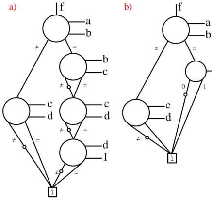
![Figure 2.10: Representations for the bit_comparator circuit in [55] (inverters are bubbles in edges)](https://thumb-us.123doks.com/thumbv2/123dok_us/10212370.2924771/62.892.243.619.165.564/figure-representations-bit-comparator-circuit-inverters-bubbles-edges.webp)