Effect of Pt bottom electrode texture selection on the tetragonality and
physical properties of Ba0.8Sr0.2TiO3 thin films produced by pulsed laser
deposition
J. P. B. Silva, K. C. Sekhar, A. Almeida, J. Agostinho Moreira, J. Martín-Sánchez et al.
Citation: J. Appl. Phys. 112, 044105 (2012); doi: 10.1063/1.4748288
View online: http://dx.doi.org/10.1063/1.4748288
View Table of Contents: http://jap.aip.org/resource/1/JAPIAU/v112/i4
Published by the American Institute of Physics.
Related Articles
Electric field induced instabilities of thin leaky bilayers: Pathways to unique morphologies and miniaturization J. Chem. Phys. 138, 024705 (2013)
Electric field-tunable BaxSr1−xTiO3 films with high figures of merit grown by molecular beam epitaxy Appl. Phys. Lett. 101, 252906 (2012)
The penetration limit of poly(4-vinyl phenol) thin films for etching via holes by inkjet printing Appl. Phys. Lett. 101, 253302 (2012)
The penetration limit of poly(4-vinyl phenol) thin films for etching via holes by inkjet printing APL: Org. Electron. Photonics 5, 270 (2012)
Numerical simulations of electrostatic interactions between an atomic force microscopy tip and a dielectric sample in presence of buried nano-particles
J. Appl. Phys. 112, 114313 (2012)
Additional information on J. Appl. Phys.
Journal Homepage: http://jap.aip.org/
Journal Information: http://jap.aip.org/about/about_the_journal
Top downloads: http://jap.aip.org/features/most_downloaded
Effect of Pt bottom electrode texture selection on the tetragonality
and physical properties of Ba
0.8Sr
0.2TiO
3thin films produced by pulsed
laser deposition
J. P. B. Silva,1,a)K. C. Sekhar,1A. Almeida,2J. Agostinho Moreira,2J. Martın-Sanchez,1,3 M. Pereira,1A. Khodorov,1and M. J. M. Gomes1
1
Centre of Physics, University of Minho, Campus de Gualtar, 4710-057 Braga, Portugal
2
Departamento de Fısica e Astronomia, IFIMUP and IN-Institute of Nanoscience and Nanotechnology, Faculdade de Ci^encias da Universidade do Porto, Rua do Campo Alegre 687, 4169-007 Porto, Portugal
3
Laser Processing Group, Instituto de Optica, CSIC, C/Serrano 121, 28006 Madrid, Spain
(Received 17 February 2012; accepted 25 July 2012; published online 28 August 2012)
The effect of platinum (Pt) bottom electrode texture on the tetragonality, dielectric, ferroelectric, and polarization switching response of pulsed laser deposited Ba0.8Sr0.2TiO3(BST) thin films has been studied. The x-ray diffraction and Raman analysis revealed the higher tetragonality of BST films when they were grown on higher (111) textured Pt layer. The properties like dielectric permittivity, polarization, switching time, and leakage currents were found to be correlated to tetragonality and orientation of the BST films. The polarization current was observed to be higher in BST films on Pt epitaxial layer and it exhibits exponential dependence on the electric field. The voltage-current measurements displayed Ohmic behavior of leakage current irrespective of Pt texture for low voltages (up to 1 V), whereas at higher voltages the conduction mechanism was found to be dependent on texture selection of bottom Pt electrode.VC 2012 American Institute of
Physics. [http://dx.doi.org/10.1063/1.4748288]
I. INTRODUCTION
Ferroelectric thin films are promising candidates for var-ious applications such as ferroelectric memories, infrared sensors, tunable microwave devices, and other integrated technologies.1Among many ferroelectrics, barium strontium titanate (BaxSr1xTiO3) is an interesting material for device applications due to their high dielectric constant, relatively low losses, and fast switching speed over a wide frequency range. Moreover, these properties can be tailored for specific applications by controlling the barium to strontium ratio. A wide variety of techniques such as sol-gel, metal-organic chemical vapour deposition, RF magnetron sputtering, and laser ablation have been employed to fabricate Ba0.8Sr0.2 TiO3 (BST) thin films and their electrical properties were extensively investigated.2–4 In fact, the properties of BST thin films have been found to depend substantially on the fabrication process, microstructure, and film thickness.3,5,6
Many researchers have continuously made attempts to enhance the properties of BST thin films by improving the crystalline quality, film-electrode interface, and interfacial strain.7,8Recently, it has been shown that textured BST thin films can be grown using the single crystal substrates like MgO and SrTiO39,10 and very thin buffered layer like SrRuO3or (La,Sr)MnO3as a bottom electrode.7,11The stud-ies on textured BST thin films revealed that their ferroelec-tric properties strongly depend upon texture selection.12 Hence, the control of crystal orientation is the easy way to tailor the properties as desired for devices. However, the control of texture selection of BST thin films on the conven-tional metal electrodes like Pt has not been much studied yet,
whereas it is important from technological point of view. It is also observed that bottom electrode directly influences the properties of BST films. However, it seems that there are no reports showing the influence of the Pt layer texture selection on the properties of the BST films. Therefore, we made an attempt to study the effect of platinum (Pt) bottom electrode texture selection on the tetragonality and physical properties of BST thin films.
In view of this, the Ba0.8Sr0.2TiO3thin films were grown using the pulsed laser deposition technique on epitaxial, highly and less (111) textured Pt layers integrated with Si substrate and their physical properties were investigated. The properties of Ba0.8Sr0.2TiO3 thin films, such as dielectric constant, leakage current, remnant polarization, and switch-ing time, were found to be closely related to the tetragonality caused by Pt bottom electrode layer texture selection. II. EXPERIMENT
The target with composition of BST was prepared by conventional solid state reaction route using raw materials of BaCO3 (Aldrich, 99%), SrCO3 (Aldrich, 98%), and TiO2 (Merck,>99%), and then, sintered at 1250C. The films were grown by pulsed laser deposition using the 248 nm line of an excimer with a frequency of 10 Hz and energy density of 5 J/cm2was focused on the target. The deposition was per-formed at 700C in an oxygen gas pressure of 0.1 mbar on commercially available platinized Si substrates with differ-ent Pt texture selection. The substrates A and C are of Neyco and B is of Radiant manufactures. The substrates A and B are SiO2/TiO2/Pt layers and substrate B is SiO2/Ti/Pt layers grown on (100) Si. Subsequently, an annealing was per-formed in air at 700C for 30 min in order to improve the
a)Electronic mail: [email protected].
crystalline structure. The thickness of films was found to be
400 nm.
The BST films and substrates were structurally character-ized using a Philips x-ray diffractometer (model PW1710), and the CuKaradiation (k¼0.154 nm). The surface morphol-ogy of BST films and platinized silicon substrates was scanned with a commercial Nanoscope III AFM system in tapping mode.
The unpolarized Raman spectra of BST films have been recorded in the backscattering geometry, at room temperature, by using an Olympus microscope and a 100objective. The 514.5 nm polarized line of an Arþlaser was used for excita-tion, with an incident power of about 16 mW impinging on the sample. The scattered light was analyzed using a T64000 Jobin-Yvon spectrometer, operating in triple subtractive mode, and equipped with liquid nitrogen cooled CCD detector in a Stokes frequency range from 200 to 800 cm1.
Gold (Au) electrodes, with diameter of 1 mm, were de-posited by thermal evaporation on the top of BST films and then annealed at 200C for 30 min in air to improve the electrode-film interface. The frequency dependence dielec-tric permittivity measurements were performed with Quad-Tech 7600b Precision LCR Meter at high measurements accuracy (60.05%), and at an applied voltage of 30 mV. The ferroelectric hysteresis loops (P-E) were traced by a
modified Sawyer-Tower circuit using a sinusoidal signal at a frequency of 1 kHz. The polarization reversal characteristics have been studied by applying square pulse, and the corre-sponding current was measured across a resistance of 100X connected in series with the samples. The leakage current of Pt/BST/Au capacitors was measured using a Keithley 617 programmable electrometer.
III. RESULTS AND DISCUSSION
A. Structural and morphological characterization of Pt substrates
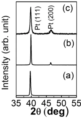
Figure1shows the x-ray diffraction (XRD) patterns of different commercial platinized substrates, used for the film deposition. As depicted in Fig. 1(a), XRD pattern of first type of Pt/TiO2/SiO2/Si substrate shows no peaks of Pt layer but (111) and this is in an agreement with manufacturer that this substrate (for convenience substrate A or epitaxial sub-strate) has the epitaxial Pt layer. In the studied range, the XRD pattern of other Pt/Ti/SiO2/Si and Pt/TiO2/SiO2/Si sub-strates consists of two peaks such as (111) and (200) related to Pt layer. The ratio of relative intensities of these two peaks was found to be 0.07 and 0.20 and the full width of half max-imum (FWHM) was equal to 0.20 and 0.42 for Pt/TiO2/ SiO2/Si (substrate B) and Pt/Ti/SiO2/Si (substrate C) sub-strates, respectively. The ratio I(200)/I(111) is 0.5 for poly-crystalline Pt (JPCDS card no. 4-0802), hereafter, the respective substrates are highly (111) (substrate B) and less (111) textured (substrate C, with poor crystalline properties of Pt layer).
Figures 2(a)–2(c) show the atomic force microscopic images of the A, B, and C substrates. The substrates A and C consist of homogenous Pt grains with mean size of 30 nm. However, the grain structure was found to be denser in the case of epitaxial substrate (Fig. 2(c)) than for substrate C. The substrate B has non-homogenous distribution of grains and also has some clusters of Pt grains with size of about 180 nm. The average root mean square (RMS) value of the surface roughness lies between 2 and 4 nm in all the sub-strates which ensures a quite planar interface between the Pt layer and the BST film.
B. Structural properties of BST thin films
1. X-ray diffraction and AFM studies
The XRD patterns of BST thin films deposited on A, B, and C substrates are illustrated in Fig. 3(a). All the BST thin films have been crystallized. The presence of clear splitting of (200) peak around 2h¼45 in the film grown on epitaxial substrate A confirms its tetragonal symmetry at
FIG. 2. AFM images of substrates (a) A, (b) B, and (c) C (1lm1lm). FIG. 1. XRD patterns of substrates (a) A, (b) B, and (c) C.
room temperature. The extended scan of XRD around 2h¼45 is shown in Fig. 3(b). The splitting of the (200) peak is not visible in the case of film grown on substrate B, but this peak is broader and asymmetric as compared with the film grown on substrate C. Hence, the decomposition of the peak was performed assuming the existence of two (002) and (200) peaks of tetragonal phase as shown in Fig.
3(b). The observed shift in the diffraction peak positions of the films with respect to bulk BST gives a small change in the lattice parameters. The lattice parameters calculated by the least-square method, tetragonality (c/a ratio), and the cell volume of thin films grown on different substrate are shown in the TableI. The tetragonality ratio is found to be the highest in the films grown on epitaxial Pt layer. Thec/a
ratio obtained for the films grown on epitaxial substrate is similar to the values found in literature for bulk BST13–15 and is slightly lower than the values obtained in the BST films grown on MgO substrate.16 For a qualitative charac-terization of the films orientation, the following equation was used:17
I0 I0100þI0101þI0111
; (1)
whereI0is equal toI/I*. TheIandI*are the intensities of a particular reflection in the film and powdered polycrystalline (JPCDS card No. 44-93), respectively. The intensity ratios are shown in TableI. It is seen that the films become more (100) textured with the increase of degree of (111) texture of Pt layer.
The AFM images of the BST thin films grown on differ-ent Pt layers reveal the similar morphology of BST thin films irrespective of Pt orientation as shown in Fig.4. All the films consist of homogenous distribution of grains with an average size of 30 nm. The average RMS value of surface roughness was found to be 6–7 nm.
2. Raman spectroscopy
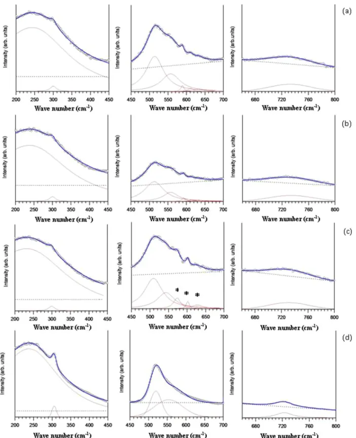
Figure5shows the room temperature unpolarized micro-Raman spectra of sintered target (inset on Fig. 5) and thin films grown on different substrates in the spectral range of 200–800 cm1. The Raman spectra of target consists of a broad peak centered at 235 cm1, a weak shoulder peak at 305 cm1, an asymmetric peak near 519 cm1, and a broad weak peak at 720 cm1. The peaks at 235, 305, 519, and 720 cm1can be assigned to A1 (2TO), E (3TOþ2LO) þ
B1, A1 (3TO), and E (4LO) phonon modes, respectively.18–20 The presence of peaks at 305 and 720 cm1in Raman spectra of the target evidences its tetragonal symmetry. The Raman spectra of films grown on different substrates consist of the referred above peaks, but their positions are slightly shifted as compared to the target. In order to analyze them in detail, a sum of independent damped oscillators, according to the gen-eral formula21 Iðx;TÞ ¼ ð1þnðx;TÞÞX N j¼1 Aoj xX2ojCoj ðX2ojx2Þ 2 þx2C2 oj (2)
was fitted to the experimental spectra. In Eq. (2), nðx;TÞ is the Bose-Einstein factor, Aoj, Xoj, and Coj are the strength,
wave number, and damping coefficient of the jth oscillator, respectively. The solid line in Fig.6shows the resultant fitting curve to the experimental data (discrete points). The wave number of the Raman active modes observed in the films is summarized in TableII. From the fitting, it can be seen three more bands in the 450–700 cm1 spectral range, which are marked with *. These bands are recognised as disorder-activated bands16,22arising from the random distribution of Ti ions, which can occupy four off-center sites in the tetragonal phase. The Ba/Sr substitution could cause local distortions, partially breaking the translational symmetry of the BT lattice. Also from the Fig.6, it is clear that the intensity of these peaks is higher for the film deposited on the less (111) textured sub-strate. This feature reveals that this Pt layer enhances disorder in the films, resulting in a decrease of tetragonality. The inten-sities of Raman modes E (3TO þ2LO)þB1 and A1 (2TO) and the ratio of their intensities were also shown in TableII. These results also suggest that tetragonality increases for more (111) textured Pt layer and is in a good agreement with XRD analysis.
C. Electrical properties
1. Dielectric and ferroelectric properties
Figure7shows the frequency dependent dielectric per-mittivity (¾r) and dielectric loss (tand) of BST films grown
TABLE I. Lattice parameters, tetragonality (c/a), cell volume, and the relative intensity ratio of peaks in BST thin films grown on different substrates.
Samples a(A˚ ) c(A˚ ) c/a Volume(A˚3)
I0 100 I0100þI0101I0111 I0 101 I0100þI0101I0111 I0 111 I0100þI0101I0111 BST/A substrate 3.984 4.011 1.007 63.7 0.78 0.22 0.00 BST/B substrate 3.981 4.002 1.005 63.5 0.12 0.68 0.20 BST/C substrate 3.991 3.999 1.002 63.7 0.09 0.65 0.26
FIG. 3. XRD patterns of BST thin films grown on substrates (i) A, (ii) B, (iii) C and (b): extended XRD scans.
on different Pt layers. Both¾rand tandhave shown a small dispersion with frequency. At high frequencies, the values of¾rand tandare found to be nearly the same in the films grown on epitaxial and highly (111) textured Pt layers. Nevertheless, the BST thin films grown on the less (111) textured Pt layer (substrate C) have much low ¾r (nearly 3 times) and high tan din the all measured frequency range. The ¾r and tandvalues obtained in the films are higher as compared to that of values reported by Pandaet al.23 and are similar to other BST films grown on platinized substrates.12,24,25
Figure8shows theP-Ehysteresis loop of BST thin films grown on different Pt layers. These loops were obtained with applying sinusoidal signal of frequency 1 kHz at room tem-perature. The values of remnant polarization (Pr), maximum polarization (Pmax), and coercive field (Ec) observed in dif-ferent films are shown in Table III. The films produced on epitaxial Pt layer (substrate A) exhibited hysteresis loops with Pr of 0.5lC/cm2, Pmax of 7.8lC/cm2 at 275 kV/cm, andEcof 16.0 kV/cm. ThePrvalue is found to be in a good agreement with the values obtained in BST films produced by other techniques.12,26 Whereas, the polarization values observed for the films grown on substrate C is much lower as compared to the values observed for the films deposited on A and B substrates and this can be attributed to the value of tetragonality. The value of the (c-a)/aratio (%) in the films grown on A, B, and C Pt layers was found to be 0.7%, 0.5%, and 0.2%, respectively. This is in consistent with the fact observed by Golovkoet al.27that BST ceramics exhibit hys-teresis loops only when the ratio (%) of (c-a)/a should be
0.19%.
2. Domain reversal process
The time dependence polarization reversal characteris-tics of the BST thin films grown on different substrates is shown in Fig.9. The bell shape curve in polarization current arises due to domains reversal. When an electric field is reversed, the domain reversal process takes place via nuclea-tion, growth, and coalescence of domains.28The whole pro-cess causes a rapid change in the polarization current. The polarization current at any time is proportional to the rate of change in fraction of domain reversal volume to the total volume of domains in the thin films. The maximum value in polarization current (im) occurs at which most of the domains are reversed and is found to be enhanced in the films grown on epitaxial substrates. The polarization during the switching (Ps) can be estimated from the area (equal to charge Q) under the transient curves using the relationQ¼2PsA(A is the area of electrode) was found to be in a good agreement with the values obtained from theP-Eloops29(TableIII).
The effect of pulse amplitude on the time dependence of polarization current transients of BST films grown on epitax-ial substrate is shown in Fig. 10. As the pulse amplitude increases from 3 to 11 V, the imvalue increases from 24 to 69 mA, whereas the tmvalues decrease from 0.61 to 0.25ls. This could be due to switching of new regions into the field direction at higher pulse amplitudes. The im values exhibit exponential dependence on the 1/E according to equation given as follows:30
im¼i0expðai=EÞ; (3)
whereaiis the activation field. The semi-log plot ofimversus 1/Eis shown in the inset of Fig.10. The activation field esti-mated from Eq.(3)is found to be 74.7 kV/cm.
3. Leakage current characteristics
Because in many applications the ferroelectrics operate under applied external electrical field, the study of leakage current mechanism is very important. Figure 11depicts the leakage current versus applied voltage (I–V) characteristics of the BST thin films grown on different substrates. We will define forward bias as the case when the top Au electrode is at a higher potential than the bottom Pt electrode and because we are interested to study the effect of Pt bottom electrode texture, the reverse bias currents will be analyzed. The I–V
characteristics were found to be slightly asymmetric, which may originate from the different work functions of Pt and Au electrodes which are about 5.6 and 5.40 eV, respectively, depending on crystallographic direction.31 In the voltage region (4–5 V), it can be seen that the leakage current increases when the Pt orientation changes from the epitaxial
FIG. 5. Raman spectra of BST thin films grown on different substrates and the BST target (inset). The arrows evidence the tetragonal peak.
FIG. 4. AFM images of BST thin films grown on substrates (a) A, (b) B, and (c) C (1lm1lm).
to less textured ones. In order to understand the conduction mechanism in BST thin films, several leakage models, such as the space-charge-limited current (SCLC), Poole-Frenkel (PF), Schottky emission (SE), and the hopping conduction, were considered.32–34 At low voltages (0–1 V), the leakage current was found to follow the Ohmic behavior, irrespective of substrate used. In the voltage range (1–5 V), the I–V de-pendence becomes non-linear that will be discussed below.
In the case of BST film deposited on substrate C, the leakage current could be well scaled with J E2, which relates to the bulk limited SCLC mechanism.34However, as is seen from Fig.12, the measurements on films of different thicknesses revealed an increase of current density with the thickness that speaks in favor of the hopping conduction mechanism.35,36In this case, the carrier injection in the film is interface controlled and the movement of the injected
carriers inside the film is through a hopping mechanism in a narrow band located in the gap and associated with some kind of structural defects. According to the hopping conduc-tion theory, the current density is described by35,36
Jsinh qEa 2kT exp Wa kT ; (4)
whereais the distance between the nearest neighbors,qthe electronic charge,Tthe temperature,Ethe electrical field,k
the Boltzmann constant, andWathe activation energy for the hopping mechanism. The plot ofJversus sinh(aV) (inset to Fig.12) shows that Eq.(4)fits well the experimental data, by adjusting the parameter a¼(qa)/(2kTw) and the fixed
a¼4 A˚ , wherewis the thickness of the layer over which the voltage drop is equal to the applied voltageV. The best fit leads to a thicknesswof 8.0 nm. This value is much lower than the film thickness (400 nm) that allows us to suggest a partial depletion of the film. These results are in a good agreement with the study of BaTiO3films
36
where the deple-tion region was suggested to be about 15 nm at room temperature.
In the case of BST film grown on epitaxial substrate A, the data showed a good fitting to two conduction mecha-nisms, namely PF and Schottky emission. The former is bulk limited that consists of field-assisted hopping from one defect to another. The later is the interface limited and caused by thermionic injection of carriers from metal elec-trode into ferroelectric. According to PF emission, the cur-rent density is as follows:32
J¼AEexp qðut ffiffiffiffiffiffiffiffiffiffiffiffiffiffiffiffiffiffiffiffi qV=pe0ew p Þ kT " # (5)
and according to Schottky emission, the current density is given by33 J¼AT2exp qðuB ffiffiffiffiffiffiffiffiffiffiffiffiffiffiffiffiffiffiffiffiffiffi qV=4pe0ew p Þ kT " # ; (6)
whereJis the leakage current density, A is a constant, E is the electric field,utis the trapped level,A**is the effective Richardson constant,Tis the temperature,qis the electronic charge, uB is the Schottky barrier height, V is the applied voltage,e0is the free space dielectric constant,eis the opti-cal dielectric constant,wis the depletion layer width, and k
is the Boltzmann constant. As it emerges from Eqs.(5)and
(6), these conduction mechanisms have similar functional dependence of current on applied voltage and one of the ways to distinguish between them is the estimated value of dielectric permittivity. Since PF conduction is a bulk mecha-nism, it is usual to assume w to be equivalent to the film thickness400 nm. In the case of Schottky model (Eq.(6)), we examined different situation from full depletion to the values of wdown to few nanometers.37 However, data han-dling in both cases of PF and Schottky emission leads to non-physical values of e. The “standard Schottky equation” relates to the situation when the mobility is high and trans-port is limited by the recombination velocity at the potential barrier maximum. In the case of reduced mobility (that could be in our case of polycrystalline film due to scattering on grain boundaries), more appropriate may be the use of Sim-mons expression(7)38 JðT;EÞ ¼aT3=2El m m0 3=2 exp /b KT expbpffiffiffiE; (7)
which takes into account both the carrier density at the potential barrier maximum near the interface and the mobil-ity which is a bulk property. As is seen from Fig.13, the data can be well fitted with the Simmons equation and give the appropriate values of e¼3.90 anduB¼0.50 eV, which are in a good agreement with the reported values for BST materials.39,40
In the case of BST film grown on substrate B, none of the mentioned models fit the experimental data in a wide voltage range. As can be seen in Fig. 14, at high voltages (2.8–5 V), the data fit to the “standard Schottky equation”(6)
withe¼3.99 anduB¼0.36 eV and suggesting full depletion. In the middle range (1–2.8 V), the most probably, several mechanisms give a considerable contribution to the leakage current.
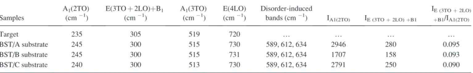
TABLE II. Optical phonon frequencies (in cm1) of Raman modes observed in BST target and in films grown on different substrates, the intensity of A1 (2TO) and E (3TOþ2LO)þB1 modes and also their intensity ratio in BST films.
Samples A1(2TO) (cm1) E(3TOþ2LO)þB1 (cm1) A1(3TO) (cm1) E(4LO) (cm1) Disorder-induced
bands (cm1) IA1(2TO) IE (3TOþ2LO)þB1
IE (3TOþ2LO) þB1/IA1(2TO) Target 235 305 519 720 … … … … BST/A substrate 245 300 515 730 589, 612, 634 2946 280 0.095 BST/B substrate 245 300 515 731 589, 612, 634 1707 158 0.093 BST/C substrate 240 300 513 730 589, 612, 634 2791 250 0.090
FIG. 7. Frequency dependent dielectric constant and tangent loss of BST films grown on different substrates.
TABLE III. Polarization values and coercive fields observed in the BST thin films grown on different substrates.
Samples Pr (lC/cm2) Ec (kV/cm) Pmax (lC/cm2) from P-Eloops Pmax (lC/cm2) from switching current BST/A substrate 0.5 16.0 7.8 8.3 BST/B substrate 0.3 16.0 6.7 6.2 BST/C substrate 0.03 29.0 0.3 0.4
FIG. 9. Time dependence polarization reversal characteristics of BST films on different substrates measure at pulse amplitude of 11 V.
FIG. 8.P-E hysteresis loops of BST films grown on substrates (a) A, (b) B, and (c) C.
FIG. 10. Effect of pulse amplitude on polarization reversal current of BST films on substrate A. The inset shows semi-log plot ofimversus 1/E.
FIG. 11. Plot of leakage current versus applied voltage of BST films on dif-ferent substrates.
FIG. 12. The plot of J versus E of films grown on substrate C with different thicknesses. The inset shows the plot ofJversus sinh(aV) for the film grown on C substrate with 400 nm thickness with linear fit.
FIG. 13. The Simmons plot of ln(J/E) versusE1/2for the films grown on substrate A.
So, we can conclude that BST films grown in the same conditions on platinized substrate of different texture showed the different conduction mechanisms. This is due to the texture selection of Pt layer. As it known, the work function of Pt depends on crystallographic direction. This is 5.93 eV for
h111idirection and decreases to 5.64 eV in the case of poly-crystalline Pt.31Thereby, when BST films were grown on epi-taxial (111) Pt layer (substrate A), the barrier height for the injection of carriers from Pt electrode into BST film was maxi-mum and the conductivity was governed by both interface and bulk properties (Simmons model). In the case of less textured Pt layers (substrates B and C), the barrier height was lower, the carriers were more easily injected into film, and conductiv-ity was governed by bulky properties of BST films.
IV. CONCLUSIONS
This work highlights the strong relationship between the texture of Pt layer and the tetragonality of the grown BST thin films. A detailed study of the influence of the bottom Pt electrode texture on the structural and ferroelectric properties of BST thin films produced by pulsed laser deposition has been performed. The XRD and Raman analysis suggest that films on epitaxial Pt layer have the highest tetragonality, which causes superior dielectric and ferroelectric properties than compared to the films on textured Pt layers. The polar-ization estimated from P-E loops agrees well with the one calculated from the domain reversal process. The polariza-tion current exhibits exponential dependence on the pulse amplitude. In the case of BST film grown on less textured Pt layer, the leakage current was observed to be governed by the hopping conduction mechanism, whereas in the case of epitaxial Pt bottom electrode, the Schottky-Simmons emis-sion was responsible for the leakage current at high fields.
ACKNOWLEDGMENTS
The author J.P.B.S. thanks FCT for the financial support (Grant SFRH/BD/44861/2008). K.C.S. thanks FCT for Post-doc Grant (SFRH/BPD/68489/2010). J.M.S. thanks FCT for the financial support (Grant SFRH/BPD/64850/2009).
1M. Dawber, K. M. Rabe, and J. F. Scott,Rev. Mod. Phys.77, 1083 (2005). 2
P. K. Sharma, G. L. Messing, and D. K. Agrawal,Thin Solid Films491, 204 (2005).
3
G. C. Jha, S. K. Ray, and I. Manna,Thin Solid Films516, 3416 (2008). 4I. Aulika, J. Pokorny, V. Zauls, K. Kundzins, M. Rutkis, and J. Petzelt,
Opt. Mater.30, 1017 (2008). 5
H.-F. Cheng,J. Appl. Phys.79, 7965 (1996). 6
C. B. Parker, J.-P. Maria, and A. I. Kingon,Appl. Phys. Lett.81, 340 (2002). 7J. Miao, L. Cao, J. Yuan, W. Chen, H. Yang, B. Xu, X. Qiu, and B. Zhao,
J. Cryst. Growth276, 498 (2005). 8
W. J. Kim, H. D. Wu, W. Chang, S. B. Qadri, J. M. Pond, S. W. Kirchoe-fer, D. B. Chrisey, and J. S. Horwitz,J. Appl. Phys.88, 5448 (2000). 9T. Delage, C. Champeaux, A. Catherinot, J. F. Seaux, V. Madrangeas, and
D. Cros,Thin Solid Films453, 279 (2004). 10
A. Sharma, Z.-G. Ban, S. P. Alpay, and J. V. Mantese,J. Appl. Phys.95, 3618 (2004).
11Z. Ma, T. Zhang, M. He, R. Pan, K. Fu, and J. Wang,J. Mater. Sci.: Mater. Electron.22, 35 (2011).
12
Z. Fu, A. Wu, and P. M. Vilarinho,Chem. Mater.18, 3343 (2006). 13
H. Y. Wang, L. Chen, H. Meng, X. M. Xiong, and J. X. Zhang,Phys. Status Solidi B246, 2392 (2009).
14D. R. Patil, S. A. Lokare, R. S. Devan, S. S. Chougule, C. M. Kanamadi, Y. D. Kolekar, and B. K. Chougule,Mater. Chem. Phys.104, 254 (2007). 15
C. Fu, C. Yang, H. Chen, Y. Wang, and L. Hu,Mater. Sci. Eng., B119, 185 (2005).
16S. Anokhin, Y. I. Yuzyuk, Y. I. Golovko, and V. M. Mukhortov, Bull. Russ. Acad. Sci. Phys.74, 1228 (2010).
17
A. Khodorov, M. Pereira, and M. J. M. Gomes,J. Eur. Ceram. Soc.25, 2285 (2005).
18
F. M. Pontes, E. R. Leite, D. S. L. Pontes, E. Longo, F. Lanciotti, T. M. Boschi, and J. A. Varela,J. Appl. Phys.91, 5972 (2002).
19
R. S. Katiyar, M. Jain, and Y. I. Yuzyuk,Ferroelectrics303, 101 (2004). 20Y. I. Yuzyuk, V. A. Alyoshin, I. N. Zakharchenko, E. V. Sviridov,
A. Almeida, and M. R. Chaves,Phys. Rev. B65, 134107 (2002). 21
J. A. Moreira, A. Almeida, M. R. Chaves, M. L. Santos, P. P. Alferes, and I. Gregora,Phys. Rev. B76, 174102 (2007).
22Y. I. Yuzyuk, J. L. Sauvajol, P. Simona, V. L. Lorman, V. A. Alyoshin, I. N. Zakharchenko, and E. V. Sviridov,J. Appl. Phys.93, 9930 (2003). 23
B. Panda, A. Roy, A. Dhar, and S. K. Ray,J. Appl. Phys. 101, 064116 (2007).
24M. Mascot, D. Fasquelle, G. Velu, A. Ferri, R. Desfeux, L. Courcot, and J. C. Carru,Ferroelectrics362, 79 (2008).
25
J. Wang, T. Zhang, N. Wan, and J. Xiang,J. Mater. Sci.: Mater. Electron
19, 1184 (2008).
26M. Kumar, S. C. Roy, M. C. Bhatnagar, S. Agarwal, and G. L. Sharma, Ferroelectrics329, 33 (2005).
27
I. Golovko, V. M. Mukhortov, Y. I. Yuzyuk, P. E. Janolin, and B. Dkhil, Phys. Solid State50, 485 (2008).
28A. Gruverman, D. Wu, and J. F. Scott,Phys. Rev. Lett.100, 097601 (2008). 29K. C. Sekhar and R. Nath,Appl. Phys. Lett.
94, 102905 (2009). 30
K. C. Sekhar, A. Nautiyal, and R. Nath,Appl. Phys. Express1, 091601 (2008).
31Electron work function of elements,” inCRC Handbook of Chemistry and
Physics, 84th ed., edited by David R. Lide (CRC Press, 2003), pp. 12–124, Internet version.
32
C. Fu, F. Pan, and W. Cai,Integr. Ferroelectr.91, 112 (2007).
33B. Chen, H. Yang, J. Miao, L. Zhao, L. X. Cao, B. Xu, X. G. Qiu, and B. R. Zhao,J. Appl. Phys.97, 024106 (2005).
34
A. A. Saif, N. Ramli, and P. Poopalan, Solid State Sci. Technol.19, 150 (2011).
35U. Boettger and V. Bryksin, Hopping Conduction in Solids(Akademie Verlag, Berlin, 1985), pp 55–73.
36
L. Pintilie, “Charge transport in ferroelectric thin films,” in Ferroelec-trics—Physical Effects, edited by Dr. M. Lallart (InTech, 2011), http://www.intechopen.com/books/ferroelectrics-physical-effects/charge-transport-in-ferroelectric-thin-films.
37
L. Pintilie, I. Vrejoiu, D. Hesse, G. LeRhun, and M. Alexe,Phys. Rev. B
75, 224113 (2007).
38J. F. Scott,J. Phys.: Condens. Matter18, R361 (2006).
39K. Sahoo, D. Misra, D. C. Agrawal, Y. N. Mohapatra, S. B. Majumder, and R. S. Katiyar,J. Appl. Phys.108, 074112 (2010).
40
S. Zafar, R. E. Jones, B. Jiang, B. White, V. Kaushik, and S. Gillespie, Appl. Phys. Lett.73, 3533 (1998).
FIG. 14. The Schottky plots of ln(J/T2) versusE0.5for the film grown on substrate B.