This is a repository copy of Mechanical strain engineering of dielectric tunability in polycrystalline SrTiO3 thin films.
White Rose Research Online URL for this paper: http://eprints.whiterose.ac.uk/128776/
Version: Accepted Version
Article:
Tkach, A., Okhay, O., Reaney, I.M. orcid.org/0000-0003-3893-6544 et al. (1 more author) (2018) Mechanical strain engineering of dielectric tunability in polycrystalline SrTiO3 thin films. Journal of Materials Chemistry C, 6 (10). pp. 2467-2475. ISSN 2050-7534
https://doi.org/10.1039/c8tc00414e
[email protected] https://eprints.whiterose.ac.uk/
Reuse
Items deposited in White Rose Research Online are protected by copyright, with all rights reserved unless indicated otherwise. They may be downloaded and/or printed for private study, or other acts as permitted by national copyright laws. The publisher or other rights holders may allow further reproduction and re-use of the full text version. This is indicated by the licence information on the White Rose Research Online record for the item.
Takedown
If you consider content in White Rose Research Online to be in breach of UK law, please notify us by
Mechanical strain engineering of dielectric tunability in polycrystalline
SrTiO
3thin films
Alexander Tkach,a Olena Okhay,a Ian M. Reaney,b Paula Maria Vilarinhoa,* a CICECO – Aveiro Institute of Materials, Department of Materials and Ceramic
Engineering, University of Aveiro, Aveiro, 3810-193, Portugal
b Functional Materials and Devices Group, Department of Engineering Materials, University
of Sheffield, Sheffield S1 3JD, England * e-mail: [email protected]
Optimizing performance using low cost scalable processing and substrates is critical if functional oxide thin films are to achieve commercialisation. Here, we present a comprehensive investigation of the role low cost Al2O3, SrTiO3, MgO substrates on the
structure, microstructure and electrical properties of SrTiO3 (ST) thin films, deposited by sol
gel processing. We demonstrate that the dielectric properties, of polycrystalline ST films depend on the strain/stress induced by the substrates. ST films deposited on Al2O3/Pt
substrates under a high tensile stress possess the smallest grain size and present the lowest value of the relative permittivity, r, with the lowest dielectric tunability. In contrast, ST films
deposited on MgO/Pt substrates, under the highest compressive stress, have the highest value
of r, tunability and polarization. It is thus demonstrated that for polycrystalline ST films the
relative permittivity and dielectric tunability may be optimised through an induced compressive stress state.
1. Introduction
Dielectric and ferroelectric based functional materials are used in wide range of important microelectronic devices. In frequency agile microwave electronics (FAME), such as phase shifters, delay lines and tunable oscillators, they are used as low dielectric loss materials. In dynamic random access memories (DRAMs) and ferroelectric random access memories
(FeRAεs) they are utilised for their high relative permittivity, r, and polarization reversal,
respectively. In general, primary objectives of research into dielectric and ferroelectric thin films are two-fold (i) to reproduce the properties of bulk polycrystals or single crystals and (ii) to explore new functionalities of these films for device applications, not observed in the counterpart bulk structures.1
Strontium titanate (SrTiO3, ST) is an incipient ferroelectric with high r at low temperature
(up to 24000) without the onset of a ferroelectric phase transition.2 In addition to the high r,
ST possesses low dielectric loss (tan) and a non-linear electric field dependence of the permittivity at low temperature.3 ST thin films usually exhibit lower
r and higher dielectric
loss than their single-crystal counterparts, as typically observed in most perovskite-type dielectrics. Reasons behind this behaviour include compositional and microstructural inhomogeneity, like the so-called “dead layer effect” at the interface,4 defects such as oxygen vacancies and related local polar regions,5 and strain.6 The properties of thin films therefore, differ from bulk and depend markedly on the surface and film/substrate interface quality which are determined by substrate type, preparation method and processing conditions.7,8 The
extent to which the surface and film/substrate interface quality impact on the properties is generally speaking dependent on the thickness with “dead layers”, for example, have a lesser effect for thicker films.
Substrates not only act as support and bottom electrodes but also play an essential role as templates for film growth. During the processing, lattice mismatch and differences in thermal expansion coefficient (TEC) can produce phase transformations and create either compressive or tensile internal stresses.9 Due to mechanical interaction with the much thicker substrate, the film is clamped in two dimensions and strain inducing effects such as: (i) anisotropy of dielectric properties (different responses in out-of-plane and in-plane directions); (ii) rotation of the spontaneous polarization relatively to the film plane (out-of-plane into in-plane polarization);10 (iii) shifting of Curie temperature TC,11 thereby dramatically changing
dielectric and piezoelectric constants; (iv) modification of type of dielectric anomaly (sharp versus diffuse)12 and critically affecting the intrinsic (optical-phonon interaction with the applied electric field) and extrinsic (lattice defects/films processing/substrate) dielectric losses.3 For example, SrRuO3, YBa2Cu3O7-x (YBCO) and amorphous buffer layers as well as
annealing treatments have been shown to decrease residual stresses and reduce loss.13,14 Thus, the evolution of strain during in situ growth and subsequent cooling is a complex process, and a clear understanding of the nature of strain in ferroelectric and incipient ferroelectric thin films is of both scientific and technological importance.
According to the theoretical prediction by Pertsev et al.,15 a ferroelectric anomaly has been
observed at room temperature in ST films grown by reactive molecular-beam epitaxy, due to in-plane stresses from the DyScO3 substrates by Haeni et al.16 The high r at room
temperature in these films (nearly 7000 at 10 GHz) and its sharp dependence on the electric field are interesting for device applications, despite the elevated loss (tan = 0.β). However,
the strain-induced enhancement in TC is attained through the utilization of a (110) DyScO3
substrate, too expensive and rare to be used in practical applications. More common substrates such as Si, MgO, Al2O3, and SrTiO3 coupled with a more scalable fabrication
process should be considered. Si/SiO2/TiO2/Pt, MgO/Pt, Al2O3/Pt, and SrTiO3/Pt substrates
(Pt is a 150 nm electrode layer in each case) are unlikely to induce strain in the film due to epitaxy and lattice mismatch, as described by Pertsev et al.15 Instead, the difference in thermal expansion coefficient between the substrates and film may be used to create tensile and compressive stresses which should influence the performance of polycrystalline as well as oriented films.
Sol-gel processing, being a chemical solution deposition method, facilitates compositional control, provides good homogeneity, lowers processing temperature within films and may be used for the fabrication of large area devices at low cost. We refer the reader to previous work, which report a systematic study on sol-gel derived ST films deposited on Si/SiO2/TiO2/Pt substrates.17 However, the effect of stress in polycrystalline sol-gel ST films
arising from the differing substrates on their dielectric performance has not been addressed. In this work, the influence of substrates such as platinized Al2O3, SrTiO3 and MgO single
crystals on the properties of 350-400 nm thick sol-gel derived ST thin films obtained at 900 °C is reported and discussed. The phase assemblage, lattice parameters and film stress (sin2 method) are evaluated by X-ray diffraction (XRD). Transmission electron microscopy (TEM) is used to inspect the microstructure of the deposited films. The dielectric and ferroelectric properties are evaluated in a metal – insulator – metal (MIM) configuration (Au/ST/Pt/substrate capacitors) in a wide frequency and temperature range. It is found that the dielectric tunability of polycrystalline ST films on platinized substrates was strongly dependent on the strain/stress induced by the substrates. Accordingly, in polycrystalline ST films, r and its tunability can be optimised via induced compressive stresses.
2. Experimental section
SrTiO3 solutions were prepared using strontium acetate (98%, ABCR Germany),
tetra-n-butyl orthotitanate (98%, MERCK Germany) as starting precursors. Acetic acid (99.8%, MERCK Germany), 1,2-propanediol (99.5%, Riedel-de Haën Germany) and absolute ethanol (99.8%, MERCK Germany) were used as solvents. Strontium acetate was initially dissolved into heated acetic acid under constant stirring to form a transparent solution. After cooling to room temperature the former solution was diluted with 1,2-propanediol and then titanium isopropoxide was added. The resultant clear solution was continuously stirred during 12 h in a
closed flask and ethanol was added as a final step. Using these solutions layers of ST were deposited on Al2O3/Pt, SrTiO3/Pt and MgO/Pt substrates by spin-coating (4000 rpm).
Subsequently the films were heated on a hot plate (T ≈ γ00 °C) for 1 min. This step was repeated after each layer to ensure complete removal of volatile species between the layers. ST thin films were annealed at Tann = 900 °C for 60 min.
Conventional XRD measurements were performed at room temperature in out-of-plane geometry using a Rigaku D-max X-ray diffractometer. The data were recorded in 0.02º step mode with β from 30º to 70º using Cu K radiation. The room-temperature in-plane incidence measurements of the ST thin films were conducted using a Philips X’Pert MPD
X-ray diffractometer, equipped with a mobile arm and X’Pert Data Collector controller software,
with Cu K radiation. The X-ray diffraction patterns were recorded with β between γ0º and 70º in 0.03º step mode using a grazing incidence angle of 3º. The X’Pert εPD Diffractometer using Cu K radiation in point focus mode that employs a crossed slit collimator (3 mm horizontal and 0.5 mm axial apertures) and a 1 mm receiving slit was also used for residual strain measurements. The diffracted beam intensity was measured for a range from -80° to 80° and a rotational angle range from 0° to 360° in 5° steps. Background and defocusing corrections were made to the diffraction patterns. Due to overlapping of the ST diffraction peaks observed in preliminary Bragg–Brentano geometry analysis, the stresses were analysed in the (211) plane because it gives the most isolated ST peak. For each /β scan subsequent analysis of the diffraction peaks was made to determine precisely the correspondent Bragg angle and therefore the lattice spacing d211 value for a certain sample tilt. The peaks were fitted by pseudo-Voigt functions using the PROFITprogram taking into account subtraction of the necessary background and K 2 contribution. The d211 values corresponding to the
maximum of the pseudo-Voigt functions and the sin2 method were used to calculate the
relative interplanar distance variation to the strain free lattice spacing d0211 value and the overall lattice strain 211. The positions of (110), (211) and (220) reflections were also used
for determination of the film lattice parameters both in in-plane and out-of-plane geometry. The structure and microstructure of the films were studied using TEM (Hitachi 9000). Dielectric measurements were conducted on MIM capacitors using Au as top and Pt as bottom electrodes. The dielectric permittivity and loss were measured using a precision LCR-meter (HP 4284A) in the temperature range of 10-300 K during heating up at a rate of 0.75 K min-1 in a He closed cycle cryogenic system (Displex ADP-Cryostat HC-2), controlled by a
digital temperature controller (Scientific Instrument Model 9650) with silicon diode thermometers. The capacitance-voltage (C-V) measurements were performed as cycle sweeps (positive voltage to negative voltage back to positive voltage) also using a precision LCR-meter HP 4284A. Hysteresis loops were measured using a ferroelectric tester (TF analyser 1000 aixACCT) at 100 Hz from 10 K to 150 K.
3. Results
3.1. Electrical Characterisation
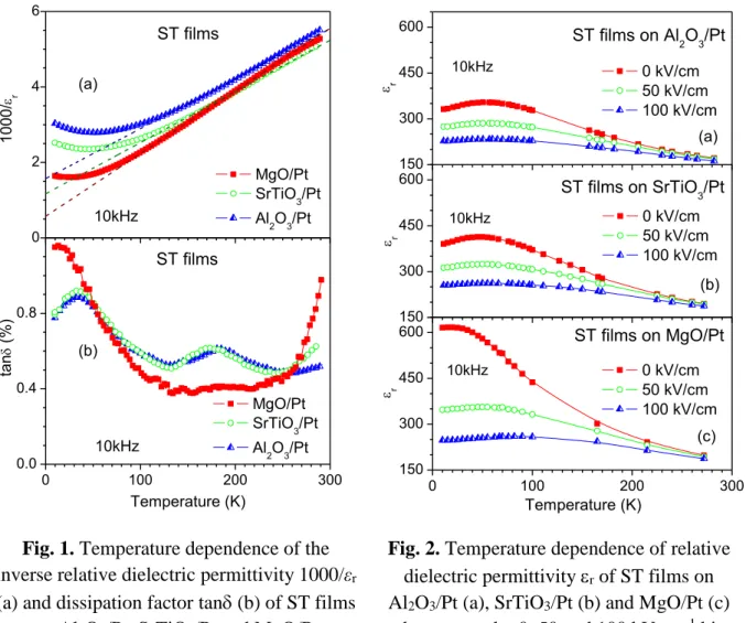
The dielectric response of 350-400 nm thick ST films deposited on different substrates is presented in Figure 1 as a function of temperature for a measurement frequency of 10 kHz. The inverse out-of-plane relative permittivity 1000/ r for ST films on all substrates above
~100 K, follows the Curie-Weiss law r = C/(T-TC), as depicted by dash lines in Figure 1a.
The Curie constant C and temperature T0 are presented in Table 1. T0 is negative for all the
films, probably due to the “dead-layer” effect previously reported,18 decreasing from about
-35 K for MgO/Pt to -86 K for SrTiO3/Pt and further to -119 K for Al2O3/Pt substrate. C varies
less dramatically within 60-76 × 103 K. Below ~100 K however, a deviation from the Curie-Weiss law is apparent and all the films exhibit a wide minimum in the 1000/ r (T) curves at
~25 - 53 K. Similar behaviour was observed in ST films prepared by excimer laser deposition on MgO/YBCO,19 deposited by inverted cylindrical magnetron sputtering on SrTiO3/YBCO
[Ref. 20] and obtained by radio-frequency magnetron sputtering on c-plane sapphire Al2O3/Pt
substrates.18Figure 1b depicts the temperature dependence of the dissipation factor tan at 10 kHz for SrTiO3 thin films deposited on Al2O3/Pt, SrTiO3/Pt and MgO/Pt. The peaks observed
at ~180 K use to be related to oxygen vacancies and observed both in ST ceramics and films.17 For all ST films, the dissipation factor is smaller than 0.012.
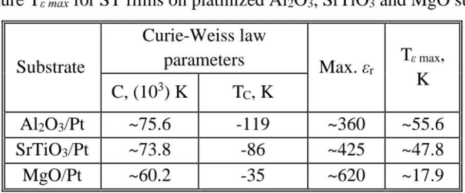
Table 1. Curie constant C and temperature TC, as well as maximum relative permittivity r
and its temperature T max for ST films on platinized Al2O3, SrTiO3 and MgO substrates.
Substrate Curie-Weiss law parameters Max. r T max, K C, (103) K TC, K Al2O3/Pt ~75.6 -119 ~360 ~55.6 SrTiO3/Pt ~73.8 -86 ~425 ~47.8 MgO/Pt ~60.2 -35 ~620 ~17.9
The temperature dependence of the relative dielectric permittivity r of ST thin films on
Al2O3/Pt, SrTiO3/Pt and MgO/Pt is found to relate to the dc electric field as plotted in Figure
2. For all the curves, a small broad peak at low temperature is presented at zero field. The highest zero-field r is obtained for ST films on MgO/Pt (~620 at 17.9 K) and the smallest on
Al2O3/Pt (~360 at 55.6 K), while for ST films on SrTiO3/Pt r exhibits an intermediate value
of ~425 at 47.8 K. The peak is smoothed with increasing electric field and shifts to high temperature, although differently for the different substrates. For Al2O3, the peak temperature
shifts to just 58.6 K under 100 kV cm-1. For SrTiO3 substrate, the shift is slightly larger to
56.1 K, whereas for magnesium oxide there is huge variation for the peak temperature from 17.9 K under zero field to 85.2 K under 100 kV cm-1. At the same time as the applied electric field increases, the r decreases. The highest dc-field effect was also observed for ST films on
MgO/Pt substrates with the highest zero-field permittivity and the lowest dc-field influence was detected for ST films on Al2O3/Pt substrates with the lowest permittivity.
Fig. 1. Temperature dependence of the inverse relative dielectric permittivity 1000/ r
(a) and dissipation factor tan (b) of ST films on Al2O3/Pt, SrTiO3/Pt and MgO/Pt
substrates at 10 kHz. Dash lines correspond to the Curie-Weiss law fits.
Fig. 2. Temperature dependence of relative dielectric permittivity r of ST films on
Al2O3/Pt (a), SrTiO3/Pt (b) and MgO/Pt (c)
substrates under 0, 50 and 100 kV cm-1 bias fields at 10 kHz. 0 2 4 6 0 100 200 300 0.0 0.4 0.8 1 0 0 0 / r 10kHz MgO/Pt SrTiO 3/Pt Al 2O3/Pt (a) ST films ta n (% ) MgO/Pt SrTiO 3/Pt Al2O3/Pt 10kHz Temperature (K) (b) ST films 150 300 450 600 150 300 450 600 10kHz 0 kV/cm 50 kV/cm 100 kV/cm r ST films on Al2O3/Pt (a) 10kHz 0 kV/cm 50 kV/cm 100 kV/cm r ST films on SrTiO3/Pt (b) 0 100 200 300 150 300 450 600 r Temperature (K) 10kHz ST films on MgO/Pt 0 kV/cm 50 kV/cm 100 kV/cm (c)
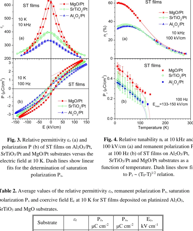
For comparison, the field dependence of the relative dielectric permittivity of ST films on all the substrates measured at 10 kHz and 10 K is presented in Figure 3a. At this temperature weak hysteresis is present in r(Edc) for all ST films, independent of the substrate. ST films on
MgO/Pt show the strongest narrow bell-shaped dependence of r on dc electric field. ST films
on Al2O3/Pt substrates reveal the lowest wide bell-shaped variation of r with Edc.
To quantify the dependence of the relative permittivity on the applied dc electric field, the relative tunability was calculated for ST films on the different substrates according to the following relation:
nr = [ r(0) – r(E)] / r(0) × 100% (1)
where r(0) and r(E) are r at zero bias and under an applied dc electric field.3 The
temperature dependence of the relative dielectric tunability (nr) obtained at 10 kHz and 100
kV/cm in ST films on Al2O3/Pt, ST/Pt and MgO/Pt is depicted in Figure 4a. At room
temperature, nr is similar for all the studied films (~3-5%), but on cooling it increases to a
different extent. For ST films on Al2O3/Pt the relative tunability reaches only ~35% at ~50 K,
for ST films on SrTiO3/Pt it reaches ~37% at ~45 K, whereas ST films on MgO/Pt present the
highest tunability of ~60% at ~15 K, whereas it is 57% at 45 K. This important result clearly indicates that the properties of polycrystalline films can be optimised by the substrate.
Variation of the polarisation under the ac electric field, P(E), of ST films on Al2O3/Pt,
SrTiO3/Pt and MgO/Pt measured at 100 Hz and 10 K is shown in Figure 3b. At this
temperature, all the studied ST films prepared on the different substrates show an s-shape hysteretic P(E) dependence with quite similar coercive field Ec of 12-15 kV cm-1, as shown in
Table 2. However, there is a stronger variation of the remanent polarization Pr from ~0.36 C
cm-2 for Al2O3/Pt and ~0.39 C cm-2 for SrTiO3/Pt to ~0.52 C cm-2 for MgO/Pt substrate
(Table 2). Moreover, the nonlinearity for ST films on MgO/Pt is higher than that of the films on Al2O3/Pt and SrTiO3/Pt substrates. Quantitatively, it can be displayed by the increase of
the saturation polarization Ps value, obtained by the linear extrapolation of data above 50 kV
cm-1 to zero field, as shown by the straight lines in Figure 3b. For MgO/Pt substrate, P
s is 1.44
C cm-2 at 10 K, as shown in Table 2. In comparison, for films on SrTiO
3/Pt and Al2O3/Pt, Ps
is 1.07 C cm-2 and 0.91 C cm-2, respectively. This behaviour apparently results in the
strengthening of polar ordering, in accordance with the enhanced r, whose values at 10 K for
Fig. 3. Relative permittivity r (a) and
polarization P (b) of ST films on Al2O3/Pt,
SrTiO3/Pt and MgO/Pt substrates versus the
electric field at 10 K. Dash lines show linear fits for the determination of saturation
polarization Ps.
Fig. 4. Relative tunability nr at 10 kHz and
100 kV/cm (a) and remanent polarization Pr
at 100 Hz (b) of ST films on Al2O3/Pt,
SrTiO3/Pt and MgO/Pt substrates as a
function of temperature. Dash lines show fits to Pr ~ (T0-T)1/2 relation.
Table 2. Average values of the relative permittivity r, remanent polarization Pr, saturation
polarization Ps and coercive field Ec at 10 K for ST films deposited on platinized Al2O3,
SrTiO3 and MgO substrates.
Substrate r Pr, C cm-2 Ps, C cm-2 Ec, kV cm-1 Al2O3/Pt 331 ~0.36 ~0.91 ~14.6 SrTiO3/Pt 391 ~0.39 ~1.07 ~13.1 MgO/Pt 616 ~0.52 ~1.44 ~12.1
With increasing temperature, the remanent polarization Pr decreases for all the studied
films, as seen from Figure 4b. ST films on MgO/Pt have the best defined hysteresis curves with the highest remanent polarization, although the loop nonlinearity diminishes on heating. The lowest values of Pr were found for ST films on Al2O3/Pt substrates, whereas for ST films
200 300 400 500 600 -150 -100 -50 0 50 100 150 -3 -2 -1 0 1 2 3 10 kHz MgO/Pt SrTiO 3/Pt Al 2O3/Pt 10 K r (a) ST films MgO/Pt SrTiO3/Pt Al 2O3/Pt 10 K E (kV/cm) 100 Hz P ( C /c m 2 ) (b) ST films 0 20 40 60 0 100 200 300 0.0 0.2 0.4 MgO/Pt SrTiO3/Pt Al 2O3/Pt 10 kHz 100 kV/cm nr (% ) ST films (a) 100 Hz Emax=133-150 kV/cm Temperature (K) P r ( C /c m 2 ) MgO/Pt SrTiO 3/Pt Al 2O3/Pt ST films (b)
on SrTiO3/Pt the Pr values are slightly higher. According to Devonshire’s theory for second
-order ferroelectric phase transitions, P ~ (T0-T)1/2 [Ref. 20], remanent polarization data from
10 to 100 K was fitted and the plots indicated by dash lines in Fig. 4b. T0 values vary from
124±2 K for Al2O3/Pt and 127±3 K for SrTiO3/Pt to 138±3 K for MgO/Pt substrate. A similar
value was obtained for ST films sputtered on SrTiO3/YBCO [Ref. 20] and related to an
electric field induced phase transition. In our case, the P(E) curves were recorded as well under the maximum electric field as high as 133-150 kV cm-1 that strongly affects the dielectric and ferroelectric response of the films.
Summarising the results shown above, one can note that ST films, deposited on the Al2O3/Pt substrates, present the lowest value of r, the weakest dependency of r on dc electric
field, the most linear P(E) behaviour (with the lowest value of Pr), and the lowest value of nr.
On the other hand, ST films deposited on MgO/Pt substrates show the highest value of r, the
highest dependency of r on dc electric field, the most well defined S-shape P(E) hysteresis
loops (with the highest value of Pr), and the highest value of nr. Finally ST films, deposited on
SrTiO3/Pt substrates have shown intermediate values. The origin of such marked modification
of dielectric properties as a function of the substrate relates to differences in the structure and microstructure of these films. Indeed it is known that phase formation, grain size21,22 and residual stress,15,16 among other structural and microstructural features affect the dielectric response of thin films. Second phases and increasing number of grain boundaries is known to suppress the overall dielectric response, originating from the polar dielectric grain cores.21,22 On the other hand, non-centrosymmetric tetragonal distortion of ST, which is known to have centrosymmetric structure in bulk, can enhance its polarizability and induce ferroelectric properties along the largest cell parameter.15,16 Hence, further structural and microstructural characterization is necessary to interpret the electrical response of the ST films.
3.2. Structure and Microstructure
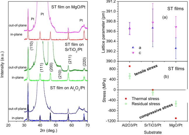
To check phase formation and assemblage, room-temperature XRD profiles of ST films deposited on different platinised substrates and annealed at 900°C were recorded both conventionally and at low incident beam angle (LIBAD) to avoid the substrate response, as shown in Figure 5. Besides the substrate and Pt reflections observed using conventional XRD in out-of-plane geometry, no secondary phase reflections were detected, indicating that all the ST films are monophasic within the XRD detection limit. No preferred orientation or texture is observed as well.
Analysing the positions of (110), (211) and (220) reflections in the profiles obtained conventionally in out-of-plane geometry and by LIBAD in in-plane geometry, a and c lattice parameters of ST films deposited on the different platinized substrates were estimated, respectively. As shown in Figure 6a, for all the ST films under study a and c values vary within the error bar around 390.69 pm, except a values for ST films on MgO/Pt substrates that lie slightly out of the error bar edge, being relatively small. Such lattice suppression can be attributed to residual stress.
Fig. 5. XRD profiles of ST films on Al2O3/Pt,
SrTiO3/Pt and MgO/Pt substrates measured in
out-of-plane and in-plane geometries. Reflections of SrTiO3 phase are marked by
corresponding indexes, while those from Pt layer are marked as Pt.
Fig. 6. (a) In-plane a (up triangles) and out-of-plane c (down triangles) lattice parameters
of ST films on Al2O3/Pt, SrTiO3/Pt and
MgO/Pt. (b) Average residual stress (open circles) and theoretical thermal stress (closed squares) for ST films on Al2O3/Pt, SrTiO3/Pt
and MgO/Pt substrates.
To obtain the residual stress values, strain measurements were conducted by the XRD sin2 method. Lattice spacings, d, of a specific (hkl) plane were measured at different tilt
angles (inclined exposure). In this work, the (211) reflection of ST was used and from the shift of this reflection as a function of tilt angle , strains were measured. Linear behaviour of the obtained strains (see Figure S1, Supplementary information) indicates a homogeneous
20 30 40 50 60 70 Pt Pt Pt in-plane out-of-plane ST film on MgO/Pt in-plane out-of-plane (2 2 0 ) (2 1 1 ) (2 1 0 ) (1 1 0 ) (1 1 1 ) (2 0 0 ) ST film on SrTiO3/Pt 2 (deg.) ST film on Al 2O3/Pt In te n s it y (a .u .) out-of-plane in-plane
Al2O3/Pt SrTiO3/Pt MgO/Pt -1200 -800 -400 0 400 800 Substrate tensile stress compre ssive stress Thermal stress Residual stress St re s s (M Pa ) ST films (b) 390.0 390.2 390.4 390.6 390.8 391.0 391.2 ST films a c L a tt ic e p a ra m e te r (p m ) (a)
stress level in all of the ST films of this study and reinforces the applicability of the sin2 method to the calculation of the stresses in these ST films. Using the average values of the obtained strain, the stress values can be calculated through the following formula:
2 0 0 sin 1 1 Y d d d hkl hkl hkl (2)
where d stands for the lattice spacing at each , d0 for the d value for =0° (perpendicular
exposure), Y and stand for the Young’s modulus and Poisson’s ratio of the film, respectively, which are taken here as Y = 265 GPa and = 0.236.23
The calculated resulting values of the average residual stress for ST films deposited on different substrates were plotted in Figure 6b. The highest tensile stress (~529 MPa) was found for ST films deposited on Al2O3/Pt substrates and the highest compressive stress (~-531
MPa) was obtained for ST films deposited on MgO/Pt substrates. The tensile stress of ST on Al2O3/Pt permits the formation of an ST lattice with almost no distortion from cubic (a ≈ c, as
shown in Figure 6a). In contrast, films on MgO are characterised by a mechanical compressive state (a < c, as shown in Figure 6a). For ST films on SrTiO3/Pt substrates a small
compressive stress (~-99 MPa) was calculated.
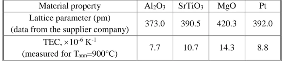
Generally in films, residual stresses come from the sum of phase transition stress, lattice misfit, and thermal stress. Since no phase transition is expected to occur either in the films or in the substrates used in this work above room temperature, the phase transition stress can be eliminated. Lattice misfit, although small, is expected between the ST film (a = 390.5 pm) and Pt electrode (a = 392.0 pm (see Table 3)). However, any stress relating to misfit should be tensile for all films, which is not the observed case.
Table 3. The lattice parameters and thermal expansion coefficients (TEC’s) of the Al2O3,
SrTiO3 and MgO substrates as well as Pt electrode.
Material property Al2O3 SrTiO3 MgO Pt
Lattice parameter (pm)
(data from the supplier company) 373.0 390.5 420.3 392.0 TEC, 10-6 K-1
(measured for Tann=900°C)
Thermal stresses that originate during cooling from the growth (Tann) to room temperature
(RT), due to differential thermal expansion coefficients (TEC’s) between film and substrate may be calculated using the following formula:
dT T T Y sub f T RT th a nn )) ( ) ( ( 1 .
(3)where f(T) and sub(T) are the temperature dependence of the TEC of ST films and
corresponding substrate (see Table 3), Y is Young’s modulus and is Poisson’s ratio of the film.24 A tensile thermal stress of ~911 MPa may be calculated for ST films deposited on non-platinised Al2O3, zero thermal stress on ST and compressive thermal stress of ~-1093 MPa on
MgO substrates. These values are plotted on Figure 6b and show the same tendency as the measured residual stress. Thus, thermal stress is the main component of the residual stress of the ST films obtained in this work.
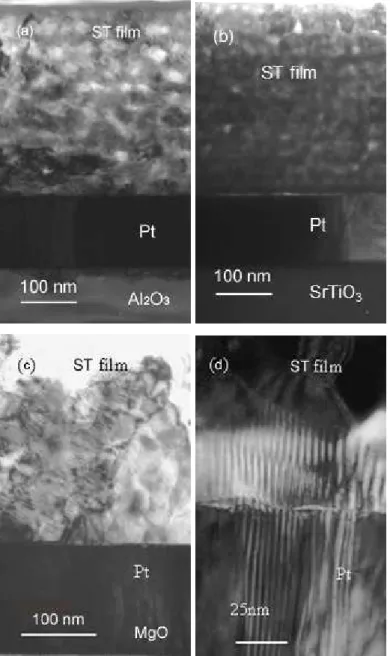
Stress relaxation however, depends on the film microstructure. The cross-section TEM images of the microstructure of ST films deposited on different platinized substrates: Al2O3/Pt, SrTiO3/Pt and MgO/Pt, are shown in Figure 7. The films (~350 nm thick) on all the
used substrates reveal dense and crack free microstructure. The micrographs evidence the polycrystalline nature of these sol-gel films with the absence of any orientation or textured features, corroborating the XRD analysis.
ST films on Al2O3/Pt (Figure 7a) and SrTiO3/Pt (Figure 7b) substrates reveal evidence thin
layers parallel to the substrate surface, from the spin-coating and crystallisation process. These films exhibit a grain size of ~30-40 nm. ST films on MgO/Pt however, exhibit no horizontal features corresponding to layer terminations (Figure 7c) and the grain size was found to be ~50-70 nm. Thus, the largest grain size is observed in ST films on MgO/Pt with the highest TEC. This statement is in agreement with the highest roughness (~4.86 nm) observed for ST films on and MgO/Pt substrates (see Figures S2 and S3, Supplementary information) using atomic force microscopy (AFM). In contrast, the smallest roughness was obtained for ST films on Al2O3/Pt (~1.21 nm) and SrTiO3/Pt (~1.35 nm) substrates.
Moreover, analysing the surface morphology by AFM the in-plane average grain size was found to be the largest as well for ST films deposited on MgO/Pt substrates (~245 nm), while ST films on Al2O3/Pt substrate show the smallest average grain size (~175 nm) similar to that
on SrTiO3/Pt substrate (~183 nm) as also shown in Figure S2, Supplementary information.
relax to lesser extent through the grain boundaries than ST films on Al2O3/Pt and SrTiO3/Pt
substrates.
The microstructure of the interfaces between ST films and the different substrates was further analysed by TEM using larger scale magnification. The most striking differences were observed in the microstructure of the interface of ST films on MgO/Pt substrates. "Line-like
defects” in ST grains are easily observed, as depicted in Figure 7d. These vertical “lines” start
at the MgO substrate and continue through the 150-nm-thick layer of Pt and cross the ST grains. This is in agreement with the compressive effect of MgO substrate on ST films. Our results indicate that when the number of grain boundaries, in which the atoms have larger free volume to relax the induced stress, is small, the stress may be relaxed via a defect formation mechanism.
Fig. 7. Cross-section TEM micrographs of ST films on Al2O3/Pt (a), SrTiO3/Pt (b) and
4. Discussion
Looking for factors, which could have an influence on the observed variation of tunability and other dielectric responses, one can suggest: stress, grain size distribution, impurities, crystallographic texture, differences in oxygen vacancy concentration, etc. However, all these factors besides those related to the grain size and stress should be quite the same for the equally deposited and processed films. Thus, the residual stress is the main factor affecting the dielectric properties of the sol-gel derived films deposited on different substrates, whereas such microstructural factor as grain size can have influence of the stress relaxation as demonstrated above. The stress/strain influence can be also expressed in general, when the thermodynamic potential G as function of polarization P, electric field E applied along P, and in-plane strain uT of the film can be expressed as:
EP S S u P P P E) , T,u G(P, 2 4 6 T T 12 11 2 (4)
where is the dielectric stiffness, and are higher order stiffness coefficients at constant stress, P is the polarization, and E is the applied electric field, while S11 and S12 are the elastic
compliances of the film at constant P.25 uT = ( f– sub) T, where f and sub are the TECs of
the film and the substrate, respectively, and T is the difference between the growth temperature Tann and room temperature. Thus, strain in polar dielectric films is one of the
most critical issues, since the dielectric properties are closely related to the ionic motions in crystal structures. As predicted from thermodynamic theory and demonstrated experimentally, strain-induced ferroelectricity can appear in epitaxial ST thin films and thus their physical properties may differ drastically from those of bulk ST crystals.15,16,26,27 However, Pertsev et
al. considered the mismatch strain-temperature phase diagram of (001)-oriented single-domain ST films grown on cubic substrates,15 whereas for the sol-gel derived ST films of this
work, mismatch strain effect is not strong and similar for all the substrates. The 150 nm of Pt electrode layer deposited on each substrate is not significant compared to the thicknesses of the substrates (~1 mm) and therefore, the differential TEC between substrate and film plays the major role. Similar conclusions were done in computational paper that also emphasizes the role of differential thermal expansion between the film and substrate from the growth (or anneal) temperature, although the calculations assumed (001)-oriented single-domain STO films.28
Thus, for our ST films on MgO/Pt, the lattice of the film is compressed on cooling from growth temperature by the thermal expansion mismatch ( MgO > ST). Therefore, a tetragonal
distortion is induced allowing the Ti ionic motions dominantly out-of-plane. As result, the dielectric properties of these films are enhanced in the parallel plate capacitor geometry, yielding the maximum polarization, permittivity and tunability. Moreover, the enhanced out-of-plane permittivity can be also explained by lower number of grain boundaries due to enlarged grain size in ST films on MgO/Pt, since grain boundaries are known to possess lower permittivity than grain bulk and to suppress the overall permittivity.21
For ST films on SrTiO3/Pt, the induce stress/strain is rather low and the out-of-plane
permittivity is lower, being diluted by dead layers and numerous grain boundaries. In the case of Al2O3/Pt substrates, grain boundaries promote as well the release of the substrate induced
tensile stress. As result, in-plane and out-of-plane lattice parameters in these films are very similar and dielectric response is just slightly lower than that for ST films on SrTiO3/Pt.
It should be noted as well that the films are polycrystalline and not so thin to avoid heterogeneous strains along the film thickness that could also lead to a flexoelectric effect contribution.29
5. Conclusions
Sol-gel derived SrTiO3 thin films were deposited on Al2O3/Pt, SrTiO3/Pt and MgO/Pt
substrates under the same processing conditions. Despite buffering by a 150 nm thick Pt layer and with a polycrystalline morphology of 350-400 nm thick ST films, the substrate is found to have a strong effect on the structure, microstructure and, consequently on the dielectric response of the films.
According to the XRD data, films on MgO/Pt have a more distorted lattice (a < c) compared to those films on Al2O3/Pt and SrTiO3/Pt (a ≈ c) which is explained by a
compressive stress/strain induced by the difference in TEC between the MgO substrate and ST film. An increase in tetragonality (c/a ratio) implies a larger displacement of Ti4+ ions and hence STO films prepared on MgO/Pt show maximum values of polarization, highest values of r with the strongest dependency on dc electric field and consequent tunability out-of-plane.
The enhanced grain growth for films on MgO/Pt also increases the out-of-plane permittivity. In contrast, the lowest polarization, permittivity and tunability were observed for ST films under tensile strain on Al2O3/Pt substrates.
As a result, variation of the tunability can be achieved by controlling the stain/stress level on the films via the choice of the substrate. Substrates inducing compressive strain/stress in
polycrystalline ST films improve the dielectric permittivity and tunability in the parallel plate capacitor geometry. The importance of these results lie in the demonstration of the possibility to design the electrical performance of ST films for applications such as tunable devices, via the use of a simple cost effective process as sol gel and commercially available substrates, without resorting to expensive and complex techniques and substrates (as DyScO3).
Acknowledgments
This work was funded by FEDER funds via Programa Operacional Factores de Competitividade – COMPETE and National funds via FCT (Fundação para a Ciência e Tecnologia) within the Project CICECO - FCOMP-01-0124-FEDER-037271 (FCT PEst-C/CTM/LA0011/2013) as well as within FCT independent researcher grant IF/00602/2013. I. M. Reaney acknowledges the support of the Engineering and Physical Sciences Research Council grant, EP/L017563/1. M. R. Soares is acknowledged for XRD analysis.
References
1 P. Zubko, S. Gariglio, M. Gabay, P. Ghosez, and J.-M. Triscone, Interface Physics in Complex Oxide Heterostructures, Annu. Rev. Condens. Matter Phys., 2011, 2, 141. 2 K. A. Müller and H. Burkard, SrTiO3: An intrinsic quantum paraelectric below 4 K,
Phys. Rev. B, 1979, 19, 3593.
3 A. K. Tagantsev, V. O. Sherman, K. F. Astafiev, J. Venkatesh and N. Setter,
Ferroelectric Materials for Microwave Tunable Applications, J. Electroceram., 2003, 11, 5.
4 C. Zhou and D. M. Newns, Intrinsic dead layer effect and the performance of ferroelectric thin film capacitors, J. Appl. Phys., 1997, 82, 3081.
5 A. A. Sirenko, I. A. Akimov, J. R. Fox, A. M. Clark, H.-C. Li, W. Si, and X. X. Xi, Observation of the First-Order Raman Scattering in SrTiO3 Thin Films, Phys. Rev. Lett.,
1999, 82, 4500.
6 T. R. Taylor, P. J. Hansen, B. Acikel, N. Pervez, R. A. York, S. K. Streiffer and J. S. Speck, Impact of thermal strain on the dielectric constant of sputtered barium strontium titanate thin films, Appl. Phys. Lett., 2002, 80, 1978.
7 J. Junquera and P. Ghosez, Critical thickness for ferroelectricity in perovskite ultrathin films, Nature, 2003, 422, 506.
8 Chang W., J. S. Horwitz, A. C. Carter, J. M. Pond, S. W. Kirchoefer, C. M. Gilmore and D. B. Chrisey, The effect of annealing on the microwave properties of Ba0.5Sr0.5TiO3
thin films, Appl. Phys. Lett., 1999, 74, 1033.
9 N. A. Pertsev, A. G. Zembilgotov, S. Hoffmann, R. Waser and A. K. Tagantsev, Ferroelectric thin films grown on tensile substrates: Renormalization of the Curie–Weiss law and apparent absence of ferroelectricity, J. Appl. Phys., 1999, 85, 1698.
10 A. Y. Emelyanov, N. A. Pertsev and A. L. Kholkin, Effect of external stress on ferroelectricity in epitaxial thin films, Phys. Rev. B, 2002, 66, 214108.
11 G. A. Rossetti, Jr., L. E. Cross and K. Kushida, Stress induced shift of the Curie point in epitaxial PbTiO3 thin films, Appl. Phys. Lett., 1991, 59, 2524.
12 A. K. Tagantsev, N. A. Pertsev, P. Muralt, and N. Setter, Strain-induced diffuse dielectric anomaly and critical point in perovskite ferroelectric thin films, Phys. Rev. B, 2001, 65, 012104.
13 H.-C. Li, W. Si, A. D. West and X. X. Xi, Near single crystal-level dielectric loss and nonlinearity in pulsed laser deposited SrTiO3 thin films, Appl. Phys. Lett., 1998, 73, 190.
14 L. A. Knauss, J. M. Pond, J. S. Horwitz, D. B. Chrisey, C. H. Muelle, and R. Treece, The effect of annealing on the structure and dielectric properties of BaxSr1-xTiO3
ferroelectric thin films, Appl. Phys. Lett., 1996, 69, 25.
15 N. A. Pertsev, A. K. Tagantsev and N. Setter, Phase transitions and strain-induced ferroelectricity in SrTiO3 epitaxial thin films, Phys. Rev. B, 2000, 61, R825.
16 J. H. Haeni, P. Irvin, W. Chang, R. Uecker, P. Reiche, Y. L. Li, S. Choudhury, W. Tian, M. E. Hawley, B. Craigo, A. K. Tagantsev, X. Q. Pan, S. K. Streiffer, L. Q. Chen, S. W. Kirchoefer, J. Levy and D. G. Schlom, Room-temperature ferroelectricity in strained SrTiO3, Nature, 2004, 430, 758.
17 O. Okhay, A. Tkach, A. Wu and P.M. Vilarinho, Manipulation of dielectric permittivity of sol-gel SrTiO3 films by deposition conditions, J. Phys. D: Appl. Phys.,
2013, 46, 505315.
18 N. A. Finstrom, J. Cagnon and S. Stemmer, Properties of dielectric dead layers for SrTiO3 thin films on Pt electrodes, J. Appl. Phys., 2007, 101, 034109.
19 T. Hirano, T. Fujii, K. Fujino, K. Sakuta and T. Kobayashi, Epitaxial SrTiO3 thin
films grown by ArF Excimer Laser Deposition, Jpn. J. Appl. Phys., 1992, 31, L511. 20 D. Fuchs, C. W. Schneider, R. Schneider and H. Rietschel, High dielectric constant and tunability of epitaxial SrTiO3 thin film capacitors, J. Appl. Phys., 1999, 85, 7363.
21 J. Petzelt, T. Ostapchuk, I. Gregora, I. Rychetsky, S. Hoffmann-Eifert, A. V. Pronin, Y. Yuzyuk, B. P. Gorshunov, S. Kamba, V. Bovtun, J. Pokorny, M. Savinov, V.
Porokhonskyy, D. Rafaja, P. Vanek, A. Almeida, M. R. Chaves, A. A. Volkov, M. Dressel and R. Waser, Dielectric, infrared, and Raman response of undoped SrTiO3 ceramics:
Evidence of polar grain boundaries, Phys. Rev. B, 2001, 64, 184111.
22 T. Ostapchuk, J. Petzelt, V. Zelezny, A. Pashkin, J. Pokorny, I. Drbohlav R. Kuzel, D. Rafaja, B. P. Gorshunov, M. Dressel, Ch. Ohly, S. Hoffmann-Eifert and R. Waser, Origin of soft-mode stiffening and reduced dielectric response in SrTiO3 thin films, Phys. Rev. B,
2002, 66, 235406.
23 J. B. Wachtman, Jr., M. L. Wheat, and S. Marzullo, A Method for Determining the Elastic Constants of a Cubic Crystal from Velocity Measurements in a Single Arbitrary Direction; Application to SrTiO3, J. Res. NBS, 1963, 67, A193.
24 M. Beihai, L. Shanshan, T. Sheng, N. Manoj, E. K. Rachel, H. Zhongqiang, and B. Uthamalingam, Residual stress of (Pb0.92La0.08)(Zr0.52Ti0.48)O3 films grown by a sol-gel
process, Smart Mater. Struct., 2013, 22, 055019.
25 A. Sharma, Z. G. Ban, S. P. Alpay, and J. V. Mantese, Pyroelectric response of ferroelectric thin films, J. Appl. Phys., 2004, 95, 3618.
26 D. Nuzhnyy, J. Petzelt, S. Kamba, P. Kužel, C. Kadlec, V. Bovtun, ε. Kempa, J. Schubert, C. M. Brooks, and D. G. Schlom, Soft mode behavior in SrTiO3/DyScO3 thin
films: Evidence of ferroelectric and antiferrodistortive phase transitions, Appl. Phys. Lett., 2009, 95, 232902.
27 R. Wordenweber, J. Schubert, T. Ehlig, and E. Hollmann, Relaxor ferro- and
paraelectricity in anisotropically strained SrTiO3 films, J. Appl. Phys., 2013, 113, 164103.
28 J. Zhang, C. V. Weiss, and S. P. Alpay, Effect of thermal stresses on the dielectric properties of strontium titanate thin films, Appl. Phys. Lett., 2011, 99, 042902.
29 A. N. Morozovska, E. A. Eliseev, M. D. Glinchuk, L.-Q. Chen, and V. Gopalan, Interfacial polarization and pyroelectricity in antiferrodistortive structures induced by a flexoelectric effect and rotostriction, Phys. Rev. B, 2012, 85, 094107.