International Journal of Emerging Technology and Advanced Engineering
Website: www.ijetae.com (ISSN 2250-2459,ISO 9001:2008 Certified Journal, Volume 3, Issue 5, May 2013)
PV System Using DC-DC Converter In A Delta Conversion
Concept
S. Niissha Begam
1, Dr. SP. Umayal
21Student of Power Electronics and Drives, Sethu Institute of Technology, Viruthunagar, India 2
Head of Power Electronics and Drives, Sethu Institute of Technology, Viruthunagar, India
Abstract—Photovoltaic (PV) systems are increasingly used
to generate electrical energy from solar irradiation incident on PV modules. PV modules are connected either in series or parallel to get high output power. Each PV cell has its own Maximum Power Point (MPP). This MPP varies with illumination, temperature, radiation and partial shading. Due to partial shading, difference between output powers of various PV modules exists. This difference leads to voltage drop in PV output power. Hence system efficiency decreases. Delta Conversion concept is introduced to overcome this problem which increases the output voltage of PV by means of using DC/DC Converter. In this proposed project SEPIC converter is used as a DC-DC converter or Delta converter. Simulation is carried out using MATLAB R2009b. PV system is widely used in terrestrial and space applications.
Keywords— Delta Converter, Maximum Power Point
(MPP), Photovoltaic, Single ended Primary Inductor Converter(SEPIC).
I. INTRODUCTION
Over the past few years conventional sources of energy results in fuel price hikes, decaying the environment leads to global warming. Hence, demand of renewable source of energy is increased compared to conventional sources.
Solar energy is one of the most readily available sources of energy. It is also the most important of the renewable sources of energy because it is non-polluting and therefore, helps in reduction of the greenhouse effect [1]-[2]. India is one of the few countries with long days and bounty of sunshine, especially in the Thar Desert region. This zone, having rich solar energy available, is suitable for using solar energy for a number of applications. In areas with same intensity of solar radiation, solar energy could be harnessed without any difficulty. Solar energy is being used in India for heating water for both industrial and domestic purposes. Solar energy can also be used to meet our electricity requirements. Through Solar Photovoltaic (SPV) cells, solar radiation gets converted into electricity. This electricity can be used as it is or that can be stored in the battery for continuous power supply. This stored electrical energy then can be used at night or when main power is decoupled from the supply. SPV can be used for a number of applications such as: domestic lighting, water heater, street lighting, water pumping, and railway signals.
A . Photovoltaic Cell
A photovoltaic cell or photoelectric cell is a semiconductor device that converts light to electrical energy by photovoltaic effect. When light shines on a PV cell, only the absorbed light generates electricity. With their newfound energy, these electrons escape from their normal positions in the atoms and become part of the electrical flow in an electrical circuit. Built in electrical field is the special property of PV cell which provides the voltage required to drive the current through an external load. Crystalline silicon PV cells are the most common photovoltaic cells in use today [3]-[9].
Usually a number of PV modules are arranged in series and parallel to meet the energy requirements. Various sizes of PV modules are commercially available. A PV module is a current delivery device whose output varies with light levels. In practical cases, due to shading of PV system over 10% will reduce the output power by more than 30% [10].
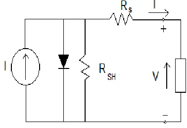
A PV array consists of several photovoltaic cells in series and parallel connections. In Series connections the voltage of the module increases whereas in parallel connection is increases the current in the array. Typically a solar cell is a current source type behavior and an inverted diode connected in parallel to it. Series resistance is due to complexity in the path of flow of electrons from n to p junction and parallel resistance is due to the leakage current.
[image:1.612.342.531.594.723.2]To maximize a photovoltaic (PV) system's output power, continuous tracking of maximum power point (MPP) of the system is necessary. The MPP depends on temperature, irradiance conditions, and the load connected.
International Journal of Emerging Technology and Advanced Engineering
[image:2.612.78.251.138.342.2]Website: www.ijetae.com (ISSN 2250-2459,ISO 9001:2008 Certified Journal, Volume 3, Issue 5, May 2013)
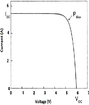
Fig 2: I-V Characteristics of A Solar Panel.
Tracking of MPP can be done by using Perturb and Observe (P&O) Algorithm and Incremental Conductance Method (ICM).
B. Perturb And Observe
The concept behind the "perturb and observe" (P&O) method is to modify the operating voltage or current of the photovoltaic panel until obtaining maximum power. For instance, if increasing the voltage to a panel increases the power output of the panel, the system continuously increase the operating voltage until the power output begins to decrease. Once this happens, the output voltage is decreased to get back towards the maximum power point. This cyclic operation continues indefinitely. Thus, the output power oscillates around a maximum power point and never stabilizes.P&O is simple to implement and thus can be implemented quickly. The major drawbacks of this method are that the power obtained oscillates around the maximum power point in steady state operation. Under rapidly varying irradiance levels and load levels it leads to wrong direction of tracking MPP.
C. Incremental Conductance
Incremental conductance considers the fact that the slope of the power-voltage curve is zero at the maximum power point, positive at the left of the MPP, and negative at the right of the MPP. The MPP is found by comparing the instantaneous conductance (I/V) to the incremental conductance (ΔI/ΔV). Once you have the MPP, the system maintains this power point unless a change in V or I occurs (caused by an external event).
If this happens, the algorithm will find the new MPP. This technique has an advantage that it can reach and maintain the MPP without losing some efficiency by having to oscillate around this point. Under rapidly changing conditions this algorithm tracks more accurately than the P&O method. The disadvantage of this method is that it can take longer to reach the MPP because the increased computation required decreases the number of perturbations to the operating voltage and current possible in a set amount of time.
II. DELTA CONVERTER
The Delta converter is a DC-DC converter. The main function of Delta Converter is to improve the decreased output voltage of PV modules. The DC-DC converter may be a Buck, Boost or Buck-Boost Converter. Here, Single Ended Primary Inductor Converter (SEPIC) is used as a Delta Converter. Conventional module-level DC-DC conversion and module level DC-DC conversion was explained in [11-18].
Fig 3: Schematic of Delta Conversion.
The figure3 shows the schematic of Delta Converter. It consists of two substrings and one SEPIC Converter.
Here, the Delta means difference. Only when difference between two strings exists, the conversion takes place i.e., the SEPIC Converter is active, otherwise it is in OFF state. Hence, it is called Delta Conversion. Therefore, low cost and low efficiency converter can be used. Also, here one converter for two strings is used compared to conventional one, where each string consists of its own DC-DC Converter. When two strings are equal the voltage is fed into the DC-DC Converter which drives the load.
[image:2.612.326.573.370.548.2]International Journal of Emerging Technology and Advanced Engineering
Website: www.ijetae.com (ISSN 2250-2459,ISO 9001:2008 Certified Journal, Volume 3, Issue 5, May 2013)
III. SEPIC CONVERTER
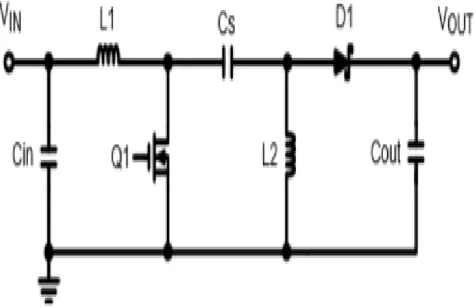
The single-ended primary-inductor converter—the SEPIC converter—is capable of operating from an input voltage that is greater or less than the regulated output voltage. Aside from being able to function as both a buck and boost, the SEPIC design also has minimal active components, a simple controller, and clamped switching waveforms which provide low noise operation. Fig3 shows the schematic of SEPIC Converter.
[image:3.612.58.296.445.599.2]The single-ended primary-inductance converter (SEPIC) is a DC/DC-converter topology that provides a positive regulated output voltage from an input voltage that varies from above to below the output voltage. This type of conversion is handy when the designer uses voltages (e.g., 12 V) from an unregulated input power supply such as a low-cost wall wart. Unfortunately, the SEPIC topology is difficult to understand and requires two inductors, making the power-supply footprint quite large. Recently, several inductor manufacturers began selling off-the-shelf coupled inductors in a single package at a cost only slightly higher than that of the comparable single inductor. The coupled inductor not only provides a smaller footprint but also, to get the same inductor ripple current, requires only half the inductance required for a SEPIC with two separate inductors. This article explains how to design a SEPIC converter with a coupled inductor.
Fig 4: Schematic of SEPIC converter.
MODE1: WHEN Q1 IS ON
When switch Q1 is turned on, current IL1 increases and the current IL2 increases in the negative direction. The Energy to increase the current IL1 comes from the input source. Since Q1 is a short while closed, and the instantaneous voltage VCS is approximately VIN, the voltage
VL2 is approximately −VIN.
Therefore, the capacitor Cs supplies the energy to increase the magnitude of the current in IL2 and thus increase the energy stored in L2. The easiest way to visualize this is to consider the bias voltages of the circuit in a dc state, then close Q1.
MODE2: WHEN Q1 IS OFF
When switch Q1 is turned off, the current ICs becomes the same as the current IL1, since inductors do not allow instantaneous changes in current. The current IL2 will continue in the negative direction, in fact it never reverses direction. It can be seen from the diagram that a negative
IL2 will add to the current IL1 to increase the current delivered to the load. Using Kirchhoff's Current Law, it can be shown that ID1 = ICS - IL2. It can then be concluded, that while S1 is off, power is delivered to the load from both L2 and L1. Cs, however is being charged by L1 during this off cycle, and will in turn recharge L2 during the on cycle.
Because the potential (voltage) across capacitor Cs may reverse direction every cycle, a non-polarized capacitor should be used. However, a polarized tantalum or electrolytic capacitor may be used in some case, because the potential (voltage) across capacitor Cs will not change unless the switch is closed long enough for a half cycle of resonance with inductor L2, and by this time the current in inductor L1 could be quite large.
The voltage drop and switching time of diode D1 is critical to a SEPIC's reliability and efficiency. The diode's switching time needs to be extremely fast in order to not generate high voltage spikes across the inductors, which could cause damage to components. Fast conventional diodes or Schottky diodes may be used.
The resistances in the inductors and the capacitors can also have large effects on the converter efficiency and ripple. Inductors with lower series resistance allow less energy to be dissipated as heat, resulting in greater efficiency (a larger portion of the input power being transferred to the load). Capacitors with low equivalent series resistance (ESR) should also be used for Cs and C2 to minimize ripple and prevent heat build-up, especially in Cs where the current is changing direction frequently.
IV. PERFORMANCE ANALYSIS
International Journal of Emerging Technology and Advanced Engineering
[image:4.612.329.564.133.298.2]Website: www.ijetae.com (ISSN 2250-2459,ISO 9001:2008 Certified Journal, Volume 3, Issue 5, May 2013)
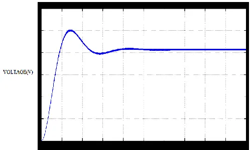
Fig 5: Output Voltage From SEPIC Converter When Two Voltages Are Different.
The Fig6 output voltage from boost converter when two voltages are different. This output voltage is used to supply the load. The output voltage obtained after simulation is 82.69V. The input voltage to the boost converter comes from the SEPIC converter output.
Fig 6: Output Voltage From Boost Converter When Two Voltages Are Different.
[image:4.612.51.287.382.514.2]The Fig7 output voltage from SEPIC converter when two voltages are equal. The output voltage obtained after simulation is 0V. Here, the SEPIC converter will be in OFF condition.
Fig 7: Output Voltage From SEPIC Converter When Two Voltages Are Equal.
The Fig8 output voltage from boost converter when two voltages are equal. This output voltage is used to supply the load. The output voltage obtained after simulation is 83.2V. The input voltage to the boost converter comes directly from the input voltage. At this condition SEPIC converter is OFF.
[image:4.612.325.575.405.554.2]International Journal of Emerging Technology and Advanced Engineering
Website: www.ijetae.com (ISSN 2250-2459,ISO 9001:2008 Certified Journal, Volume 3, Issue 5, May 2013)
V. CONCLUSION
A novel module-level DC/DC SEPIC converter concept has been introduced in this paper. In this delta-conversion concept two DC/DC SEPIC converters along with three modules are connected in order to take into account of shaded string. Hence, the decreased output voltage of PV module can be improved. This concept is
Implemented for a steady state condition. The future focus of this work includes the use of PV module for different shadings of voltage.
REFERENCES
[1] Henk Jan Bergveld, Dick Büthker, Cristiano Castello, Toby Doorn, Adrie de Jong, Ralf van Otten, and Klaas de Waal,‘Module-Level DC/DC Conversion for Photovoltaic Systems: the Delta-Conversion Concept ’,IEEE 2011.
[2] ‘Global Market Outlook for Photovoltaics until 2015’, European Photovoltaic Industry Association, EPIA, May 2011, www.epia.org. [3] E.R. Weber, ‘Aussichten der PV in Deutschland und Global’, presented at 26th Symposium Photovoltaic Solar Energy, Bad Staffelstein, Germany, March 2-4, 2011.
[4] ‘Planning and Installing Photovoltaic Systems – A Guide for Installers, Architects and Engineers’, 2nd Edition, Earthscan, London, United Kingdom, 2008.
[5] H.J. Bergveld, D. Büthker, C. Castello, T.S. Doorn, A. de Jong, R. van Otten, K. de Waal, ‘Module-level DC/DC Conversion for Photovoltaic Systems’, in Proc. IEEE International Telecommunications Energy Confererence, Amsterdam, the Netherlands, October 9-13, 2011, pp. 1-9.
[6] H. Häberlin, ‘Photovoltaik – Strom aus Sonnenlicht für Verbundnetz und Inselanlagen’, 2nd Edition, Electrosuisse Verlag, Chur, Switserland, 2010.
[7] M.G. Villalva, J.R. Gazoli, E.R. Filho, ‘Comprehensive Approach to Modeling and Simulation of Photovoltaic Arrays’, IEEE Trans. On Power Electronics, vol. 24, no. 5, May 2009, pp. 1198-1208. [8] W. Herrmann, W. Wiesner, W. Vaaßen, ‘Hot Spot Investigations on
PV Modules – New Concepts for a Test Standard and Consequences for Module Design with Respect to Bypass Diodes’, in Proc. 26th IEEE Photovoltaic Specialist Conference, Anaheim, USA, September 29-October 3, 1997, pp. 1129-1132.
[9] M. Calais, J. Myrzik, T. Spooner, V.G. Agelidis, ‘Inverters for Single-Phase Grid Connected Photovoltaic Systems – An Overview’, in Proc. IEEE Power Electronics Specialist Conference, Cairns, Australia, June 24-27, 2002, pp. 1995-2000.
[10] J.M.A. Myrzik, M. Calais, ‘String and Module Integrated Inverters for Single-Phase Grid Connected Photovoltaic Systems – A Review’, in Proc. IEEE Bologna PowerTech Conference, Bologna, Italy, June 23-26, 2003.
[11] N. Chaintreuil, F. Barruel, X. Le Pivert, H. Buttin, J. Merten, ‘Effects of Shadow on a Grid-Connected PV System’, in Proc. 23rd European Photovoltaic Solar Energy Conference, Valencia, Spain, September 2008, pp. 3417-3421.
[12] B. Burger, B. Göldi, S. Rogalla, H. Schmidt, ‘Module-Integrated Electronics – An Overview’, in Proc. 25th European Photovoltaic Solar Energy Conference, Valencia, Spain, September 2010, pp. 3700-3707.
[13] G. Bettenwort, T. Bülo, C. Merz, J. Laschinski, S. Thon, S. Zanger, ‘Benchmarking the Different PV System Concepts Focussing on Their Total Cost of Ownership’, in Proc. 25th European Photovoltaic Solar Energy Conference, Valencia, Spain, September 2010, pp. 3708-3714.
[14] G.R. Walker, P.C. Sernia, ‘Cascaded DC-DC Converter Connection for Photovoltaic Modules’, IEEE Trans. On Power Electronics, vol. 19, no. 4, July 2004, pp. 1130-1139
[15] E. Roman, R. Alonso, P. Ibañez, S. Elorduizapatarietxe, D. Goitia, ‘Intelligent PV Module for Grid-Connected PV Systems’, IEEE Trans. On Industrial Electronics, vol. 53, no. 4, August 2006, pp. 1066-1073.
[16] N. Femia, G. Lisi, G. Petrone, G. Spagnuolo, M. Vitelli, ‘Distributed Maximum Power Point Tracking of Photovoltaic Arrays: Novel Approach and System Analysis’, IEEE Trans. On Power Electronics, vol. 55, no. 7, July 2008, pp. 2610-2621. [17] L. Zhang, K. Sun, I. Xing, L. Feng, H. Ge, ‘A Modular
Grid-Connected Photovoltaic Generation System Based on DC Bus’, IEEE Trans. On Power Electronics, vol. 26, no. 2, February 2011, pp. 523-531.
[18] B. Liu, S. Duan, T. Cai, ‘Photovoltaic DC-Building-Module-Based BIPV System – Concept and Design Considerations’, IEEE Trans. On Power Electronics, vol. 26, no. 5, May 2011, pp. 1418-1429. [19] S.B. Kjaer, J.K. Pedersen, F. Blaabjerg, ‘A Review of Single-Phase
Grid-Connected Inverters for Photovoltaic Modules’, IEEE Trans. On Industry Applications, vol. 41, no. 5, September/October 2005, pp. 1292-1306.
[20] R.W. Erickson, D. Maksimović, ‘Fundamentals of Power Electronics’, 2nd edition, Springer, 2011
AUTHORS
Niissha Begam.S is a post graduate student pursuing Power Electronics And Drives from Sethu Institute of Technology under Anna University, Chennai. Her area of interest is in the field of solar applications.