Advanced coatings through pulsed
magnetron sputtering
Kelly, PJ, Hisek, J, Zhou, Y, Pilkington, RD and Arnell, RD
http://dx.doi.org/10.1179/026708404225010702
Title
Advanced coatings through pulsed magnetron sputtering
Authors
Kelly, PJ, Hisek, J, Zhou, Y, Pilkington, RD and Arnell, RD
Type
Article
URL
This version is available at: http://usir.salford.ac.uk/1562/
Published Date
2004
USIR is a digital collection of the research output of the University of Salford. Where copyright
permits, full text material held in the repository is made freely available online and can be read,
downloaded and copied for noncommercial private study or research purposes. Please check the
manuscript for any further copyright restrictions.
Published by Maney Publishing (c) IOM Communications Ltd
ADVANCED COATINGS THROUGH PULSED
MAGNETRON SPUTTERING
P. J. Kelly, J. Hisek, Y. Zhou, R. D. Pilkington and R. D. Arnell
Pulsed magnetron sputtering (PMS) has become established as the process of choice for the deposition of dielectric materials for many applications. The process is attractive because it offers stable arc free operating conditions during the deposition of, for example, functional films on architectural and auto-motive glass, or antireflective/antistatic coatings on displays. Recent studies have shown that pulsing the magnetron discharge also leads to hotter and more energetic plasmas in comparison with continuous dc discharges, with increased ion energy fluxes delivered to the substrate. As such, the PMS process offers benefits in the deposition of a wide range of materials. The present paper describes three examples where PMS has led to either significant enhancement in film properties or enhanced process flexibility: in low friction titanium nitride coatings, in Al doped zinc oxide transparent conductive oxide coatings sputtered directly from powder targets and in thin film photovoltaic devices based on copper (indium/gallium) diselenide. These
examples demonstrate the versatility of PMS and open up new opportunities for the production of advanced
coatings using this technique. SE/499
The authors are in the School of Computing Science and Engineering, University of Salford, Salford M5 4WT, UK ([email protected]). Based on a presentation at the meeting on ‘Pulsed plasma process-ing’ held at Salford University on 17 September 2003. Accepted 3 December 2003.
Keywords: Pulsed magnetron sputtering, Titanium nitride, Al doped zinc oxide, Thin film photovoltaic devices, Copper (indium/gallium) diselenide
#2004 IoM Communications Ltd. Published by Maney for
the Institute of Materials, Minerals and Mining.
INTRODUCTION
Pulsed magnetron sputtering (PMS) is widely recog-nised as an enabling technology, particularly for the deposition of dielectric materials.1 – 8 Pulsing the
magnetron discharge in the midfrequency range (20 – 350 kHz) alleviates the chief problem associated with the continuous dc reactive sputtering of such materials, namely the occurrence of arc events at the target. This is achieved through the discharging of the poisoned regions on the target during the reverse voltage or ‘pulse off’ phase. The correct selection of pulse parameters (frequency, duty, reverse voltage) can result in extended arc free operating conditions, even during the deposition of highly insulating materials.4 The suppression of arcs stabilises the
deposition process and reduces the incidence of defects in the film. Consequently, films of, for example, alumina, titania and silica, can be produced by pulsed sputtering with very much enhanced structural, electrical and optical properties, in com-parison with films produced by continuous dc processing.5,6 The pulsed sputtering technique is
now being exploited commercially in large area multiple magnetron systems for many applications, including solar control and low emissivity coatings, barrier layers on packaging, flat panel displays and solar cells. Again, very long term process stability, reduced defect densities, improved film properties and enhanced dynamic deposition rates have been reported for these systems.7,8
Recent Langmuir probe studies have shown that pulsing the magnetron discharge also significantly modifies the characteristics of the deposition plasma.9,10 For example, increased plasma densities
and electron temperatures have been measured adjacent to the substrate in pulsed discharges.
Therefore, higher ion energy fluxes can be transported to the growing film. Additionally, mass spectrometry studies of the distribution of ion energies at the substrate in an asymmetric bipolar pulsed dc magne-tron discharge have identified the existence of popu-lations of ions whose energies can be directly related to distinct phases or features within the target voltage waveform.11Clearly, the increased flux and energy of
the particles incident at the substrate may also contri-bute to the observed improvements in the structure and properties of films produced by pulsed process-ing. Furthermore, these benefits are not limited to dielectrics but can be exploited in the deposition of new, advanced coating materials. The present paper describes three examples where use of the PMS process has led to either significant enhancement in film properties or enhanced process flexibility:
(i) low friction titanium nitride (TiN) coatings (ii) Al doped zinc oxide transparent conductive
oxide (TCO) coatings sputtered directly from blended powder targets
(iii) thin film photovoltaic devices based on copper indium diselenide (CIS).
Low friction TiN coatings
Published by Maney Publishing (c) IOM Communications Ltd
Al doped zinc oxide TCO coatings sputtered directly from blended powder targets
Mixed zinc oxide and alumina powder targets have been used to produce transparent semiconductive films on glass by PMS. Resistivities of the order of 1023Vcm were obtained after annealing, without deterioration of the coating to substrate adhesion. The results to date demonstrate that the PMS of doped ZnO films from powder targets is a flexible, novel technique for the deposition of high quality TCO materials.13,14
Thin film photovoltaic devices based on CIS
These have demonstrated exceptional energy conver-sion efficiencies and a high tolerance to radiation damage. The opto-electronic properties of this complex material are a function of its defect structure and therefore the material growth parameters. To date, the reproducible growth of CIS has been problematic; it has always been necessary to use post-deposition processing to obtain material with the required properties. Initial work with PMS has produced single phase, stoichiometric p-type films with resistivities in the range 5Vcm and excellent optical absorption properties.
EXPERIMENTAL
TiN coatings were deposited by continuous and pulsed reactive magnetron sputtering in a Teer Coatings Ltd UDP250 rig.12 Sputtering took place from a single
3006100 mm, 99.5% pure titanium target. The reac-tive sputtering process was controlled by optical emissions monitoring (OEM), using conditions selected to produce stoichiometric TiN coatings, based on previous experience.12The magnetron was driven by a
5 kW Advanced Energy1 MDX dc power supply. When operating in pulsed mode, this supply was connected in series with an Advanced Energy SPARC-LE 20 pulse unit. The SPARC-LE 20 con-verts the dc input from the MDX into an asymmetric bipolar pulsed dc output to the magnetron, with the pulse frequency fixed at 20 kHz. The SPARC-LE 20 has a duty cycle of 90%, i.e. each pulse on cycle, during which sputtering takes place, has a duration of 45ms, and each pulse off cycle, during which the target voltage is reversed, has a duration of 5ms. During pulse off, the target voltage is reversed to 10% of the nominal pulse on voltage.
Coatings were deposited onto various substrate materials, including silicon wafers and tool steel, to suit different analytical techniques. All substrates were ultrasonically precleaned in propanol. Prior to the deposition of the TiN coatings, the substrates were also dc sputter cleaned at21000 V for 15 min. The coatings were characterised in terms of their structures and properties using a range of analytical and measurement techniques, including SEM, elec-tron probe microanalysis (EPMA), X-ray diffraction (XRD), microhardness testing and surface profilo-metry. The tribological properties of the TiN films were investigated by thrust washer friction and wear testing15 and scratch adhesion testing.
The ZnO : Al and CIS coatings were both deposited in a rig specifically designed for powder target use.13
A single 180 mm dia. unbalanced magnetron was installed in the base plate of the chamber in the
‘sputter up’ configuration. The magnetron was built at Salford and utilises rare earth magnets to give high field strengths at the target (2.2 kG maximum). The substrate holder was positioned directly above the magnetron at a separation of 120 mm. The substrate holder could be rf biased, if required. A 500 W radiant heater was also installed in the rig, which could be positioned, post-deposition, to face the coated sub-strate. This allowed annealing of the coatings to take place in controlled atmospheres at temperatures of up to 500uC. Finally, a dummy magnetron was installed in the chamber roof vertically opposed to the magne-tron. This dummy device only included an outer ring of magnets and was installed to produce a closed magnetic field across the chamber, maximising the ion to atom ratio incident at the substrate.16 The rig is
shown schematically in Fig. 1.
The Al doped – ZnO powder blends were made by mixing appropriate quantities of zinc oxide and aluminium oxide powders in a rotating drum for several hours. For each material, the average particle size was 5mm, and the purity was 99.99%. Initial batches were produced with a dopant concentration of 4 wt-%alumina. Following blending, approxi-mately 60 g of powder was evenly distributed across the surface of a copper backing plate on the magne-tron to form a target. The backing plate had been recessed to a depth of 2 mm to allow a reasonable target thickness to be produced. The powder was lightly tamped down to produce a uniform thickness and surface to the target. No further processes were involved in target production. To demonstrate the flexibility of this technique, subsequent experiments have been carried out in the same manner using zinc oxide blended with oxides of tin, antimony, indium and gallium.14Tin doped indium oxide (ITO) blends
have also been produced and tested.
In all cases, coatings were deposited onto glass microscope slides by PMS using an Advanced Energy Pinnacle Plus magnetron driver supply. This unit, which is also an asymmetric bipolar supply, can
1 Schematic representation of powder target rig
158 Kelly et al. Advanced coatings through PMS
Published by Maney Publishing (c) IOM Communications Ltd
operate at pulse frequencies of up to 350 kHz at duties in the range 50 – 100%. The glass substrates were rf sputter cleaned prior to deposition (see Kelly
et al.13 and Zhou et al.14 for full run details). The
coatings were subsequently analysed by SEM, EPMA and XRD. The electrical properties were investigated using a four point probe and the optical properties were investigated using an Aquila Instruments nkd8000 spectrophotometer.
The starting material for the CIS coatings was powder prepared from crushed stoichiometric single and polycrystalline CIS ingots which were grown in what is a standard technique at Salford Univer-sity.17,18 This powder was sieved to particle sizes in
the range 0.05 – 1 mm, and was formed into a target in the manner described above. The composition of the starting powder was 29Cu – 17In – 54Se (at.-%), as determined by EPMA. Coatings were again deposited onto glass substrates by PMS using the Pinnacle Plus supply at a range of frequencies and duties. The coatings were analysed using the techniques described previously.
RESULTS TiN coatings
EPMA analysis of the continuous and pulsed dc TiN coatings confirmed that both sets of coatings had stoichiometric compositions. Both sets of coatings had similar hardness values, as measured using a Fischerscope H100 with a 50 mN load (typically
y26 GPa), and similar roughness values, as mea-sured using a Talysurf 10 (Ra~0.30 – 0.38 mm for
coatings deposited onto tool steel). XRD analysis indicated that the strong (111) texture of the continuous films was shifted to a weaker (002) texture in the pulsed films.12
The most interesting results, though, for the TiN films were the relative tribological properties of the continuous and pulsed films. Figure 2 compares the friction response of these films in unlubricated thrust washer tests, running against phosphated shim counterfaces (full test conditions are summarised in the figure caption). In these tests, the pulsed films repeatedly gave significantly lower coefficients of friction than did the continuous films. Indeed, in the example shown, the average coefficient of the pulsed
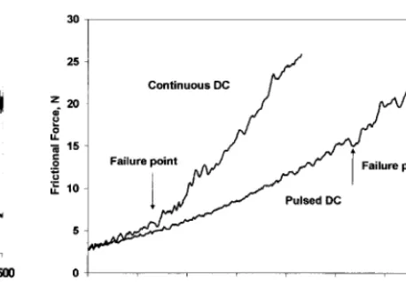
film is 0.09, compared with 0.34 for the continuous film. No measurable wear was observed on the surface of either film after a test duration of 60 min. The pulsed films also performed notably better than the continuous films during scratch adhesion testing. A comparison of the friction forcev.normal load for an example of each film type is shown in Fig. 3. The critical load for the continuous film was 24 N, whereas the pulsed film did not fail until the normal load reached 65 N (again, full test conditions are summarised in the figure caption).
Examination of these films by high resolution SEM revealed significant structural differences in the pulsed and continuous films. Figure 4 shows exam-ples of micrographs of the surfaces of TiN coatings deposited onto silicon wafers. The pulsed films are denser, smoother and have fewer voids than the continuous films.
Doped ZnO coatings
[image:4.595.279.508.38.197.2]The magnetron discharge readily ignited under the operating conditions chosen for the deposition of the ZnO : Al coatings (pulse frequency 350 kHz, duty 62%, target current 2 A, pressure 0.2 Pa). The process proved stable, with no problems such as outgassing or arcing being observed. Figure 5 shows a SEM micrograph of the fracture section of a typical ZnO : Al coating, deposited using the conditions described above. The coating has a dense columnar structure and appears to be defect free. Based on Fig. 5, the coating deposition rate was estimated to be 500 nm h21. EPMA analysis indicated that the coat-ings contained approximately 2 wt-%Al, i.e. close to the composition of the target (4 wt-%Al2O3).
The coatings were post-deposition annealed at reduced pressure in nitrogen at 470uC for 2 h. Prior to annealing, the coatings were highly insulating. However, following this process, resistivities of
v361023Vcm were recorded. XRD analysis
indi-cated that the annealed coatings had strong (002) textures. Optical transmission spectra for examples of the ZnO : Al coatings are shown in Fig. 6. It is apparent from this figure that annealing the coatings has shifted the absorption edge towards shorter wave-lengths, i.e. higher band gap energies. This process has also increased the average and peak visible
2 Frictional response from unlubricated thrust washer testing of TiN coatings deposited by continuous dc and pulsed dc reactive magnetron sputtering (normal load 100 N; rotation speed 30 rev min21
; counterface phosphated shim, 55Rockwell C)
Published by Maney Publishing (c) IOM Communications Ltd
transmission of the coatings. The average visible transmission of the as deposited coatings was 86.2% (90% peak), compared with 88.7% (92% peak) for the annealed coatings.
CIS coatings
Once again, no problems were observed sputtering the powder targets in pulsed dc mode, with stable
discharges being achieved over a wide range of frequencies and duties. SEM examination of the coatings showed they were uniform, fully dense and pinhole free. By way of example, Fig. 7 is a SEM micrograph showing the fracture section of a CIS coating deposited onto a glass substrate. As one of the major issues in the fabrication of CIS thin films, the composition of the samples has been analysed by EPMA. All samples showed near stoichiometry, with the average composition being 24.5 – Cu – 24.5In – 51Se (at.-%).
Analysis of the electrical properties of these coat-ings showed that they were p-type semiconductors with resistivity values of the order of 5Vcm. Optically, these coatings are highly absorbing across the visible spectrum and into the IR spectrum. This is evidenced in Fig. 8, which shows the transmission spectra from 350 to 1700 nm for a typical example of the CIS coatings deposited by PMS from a powder target.
DISCUSSION
PMS has become well established as a highly effective deposition technique with numerous commercial applications. To date, though, most of these applica-tions involve the deposition of dielectric materials.
5 SEM micrograph of fracture section of ZnO – 2Al (wt-%) coating deposited on glass substrate by PMS from blended powder target (ZnO – 4 wt-%Al2O3)
6 Optical transmission spectra for ZnO – 2Al (wt-%) coatings before and after annealing (pure nitrogen at 420uC for 1 h)
a b
4 High resolution SEM micrographs showing surface topography of TiN coating deposited onto silicon wafer by a con-tinuous dc reactive magnetron sputtering,b pulsed dc reactive magnetron sputtering
7 SEM micrograph of fracture section of CIS coating deposited onto glass substrate by PMS from CIS powder target
160 Kelly et al. Advanced coatings through PMS
Published by Maney Publishing (c) IOM Communications Ltd
However, as discussed in the present paper, the benefits of utilising this technology extend well beyond this category of materials.
Taking the first example, the production of TiN coatings with coefficients of friction v0.1 in
un-lubricated tests is a remarkable result, and demon-strates the enhancement in properties that can be achieved through the use of pulsed processing. As stated earlier, TiN and its derivatives (TiAlN, etc.) are not known as low friction materials.19Coefficients of
friction would not normally be lower than, say, 0.3 for these materials in any form of unlubricated test. The enhancement in the tribological properties of the films grown by pulsed processing can be attributed to the significant structural modifications observed in these coatings. The exact mechanisms by which these changes have been brought about are not yet known, but may, perhaps, be related to the increased ion energy flux known to be delivered to the substrate during pulsed processing.11 The shift to a (200)
tex-ture in the pulsed TiN films supports this hypothesis, as this has been observed to occur elsewhere following high energy bombardment and has also been associ-ated with enhanced mechanical properties.20
The deposition of doped zinc oxide coatings from blended powder targets is an example of how pulsed processing can bring enhanced process flexibility. As a consequence of using pulsed dc power to sputter oxide targets directly, no reactive sputtering control system is required, and the complexities of rf matching networks are avoided. These targets will not actually sputter using continuous dc power, as it is not possible to initiate a discharge. In fact, it is difficult to initiate a discharge even using pulsed dc at pulse frequencies below approximately 200 kHz. However, above this frequency, a stable discharge can be readily ignited and sputtering can take place directly from the oxide blends with no evidence of arcing or outgassing. The reason for the existence of an apparent ‘cut off’ frequency is not known. However, it is believed to be related to the nature of the target voltage waveforms. A feature of the Pinnacle Plus supply is a positive voltage overshoot at the beginning of the pulse off period. The magnitude of this voltage increases with pulse frequency, as can be seen in Fig. 9, which compares the target voltage waveform from this supply at both 140 kHz and 350 kHz pulse frequencies. At the lower frequency, the magnitude of the overshoot voltage is approxi-mately 300 V, whereas at 350 kHz, this reaches 600 V. It is postulated that these significant voltage
overshoots at the higher frequency range of the power supply (i.e. w200 kHz) aid plasma ignition with
poorly conducting targets.
Doped zinc oxide coatings are attracting consider-able interest as competitors for the most widely used TCO coating, namely ITO.21 – 24The dopant materials
are used to modify the electrical and optical properties of the TCO coatings. The choice and concentration of dopant are critical to the film performance. While solid targets are limited to one composition per target, powder targets offer an infinite variety of composi-tions. Furthermore, multiple dopant compositions, giving tailored film properties are readily achievable. Although doped zinc oxide coatings have been produced elsewhere by pulsed sputtering21,24 and
from sintered powder targets,22 the authors believe
this is the first time that blended oxide powder targets and pulsed dc processing have been used in combina-tion. The film properties presented here bear compar-ison with published data for ZnO : Al coatings produced by other techniques21 – 24 and, while this
may not be a production technique, this approach provides an ideal means of screening candidate materials and identifying optimum compositions.
The deposition of CIS coatings directly from a CIS powder target using PMS is also unique. CIS and the related copper indium gallium diselenide (CIGS) are very promising absorbent semiconductors for use in high efficiency photovoltaic applications. They pos-sess the highest absorption coefficients known.25 To
date, solar panels using these materials reached a stabilised efficiency of 10 – 12%. However, there is a great performance discrepancy between laboratory solar cells and commercial modules. Several research groups have achieved individual solar cell devices with efficiencies over 18%. This mismatch is mainly the result of the complexity of the material and the resulting requirements for its fabrication. To deposit stoichiometric thin films and to control the crucial properties, research and module fabrication tend to concentrate on a three stage evaporation process. A major problem is the incorporation of selenium to achieve stoichiometry and the desired crystal struc-ture, and further annealing steps are always neces-sary. The ability to deposit stoichiometric coatings directly from a powder target in a single stage process is a major step forward in this area. Furthermore, the coatings have dense, defect free structures and the necessary electrical and optical properties to be incorporated into high performance photovoltaic devices. Their high resistance to radiation damage
8 Optical transmission spectra for CIS coating deposited onto glass substrate by PMS from CIS powder target
Published by Maney Publishing (c) IOM Communications Ltd
makes them particularly attractive for use in space applications.
CONCLUSIONS
Although PMS has tended until now to be associated with the deposition of dielectric materials, the benefits offered by pulsed processing in comparison with continuous processing extend well beyond this class of materials. Examples presented here demonstrate the enhanced film properties and enhanced process flexibility that can be achieved through the use of pulsed processing. The production of low friction TiN coatings, doped zinc oxide coatings from blended oxide powder targets and dense, stoichiometric CIS coatings directly from a CIS powder target all represent important steps forward in coating techno-logy. Furthermore, they point the way to the production of new generations of advanced coating materials through the use of pulsed processing.
ACKNOWLEDGEMENTS
The present paper combines the results of several projects. The authors would like to acknowledge the contributions made by current and former colleagues at Salford University, including Dr C. F. Beevers, Dr P. S. Henderson, Mr Geoff France and Dr Chester Faunce. Furthermore, we should like to acknowledge that the high resolution microscopy presented in the present paper was carried out in the Center for Microanalysis of Materials, University of Illinois, which is partially supported by the US Department of Energy under grant DEFG02-91-ER45439.
REFERENCES
1. s. schiller,k. goedicke,j. reschke,v. kirchoff,s. schneider
andf. milde:Surf. Coat. Technol., 1993,61, 331.
2. p. j. kelly,o. a. abu-zeid,r. d. arnellandj. tong:Surf. Coat. Technol., 1996,86 – 87, 28.
3. r. a. scholl:Surf. Coat. Technol., 1998,98, 823.
4. p. j. kelly,p. s. henderson,r. d. arnell,g. a. rocheand d. carter:J. Vac. Sci. Technol., 2000,A18, 2890.
5. j. o’brienandp. j. kelly:Surf. Coat. Technol., 2001,142 – 144,
621.
6. j. o’brien,p. j. kelly,j. w. bradley,r. hallandr. d. arnell:
Proc. 45th S.V.C. Tech. Conf., Florida, 306 – 311; 2002, Society of Vacuum Coaters, Albuquerque, New Mexico.
7. g. brauer, j. szczyrbowski and g. teschner: Surf. Coat. Technol.,94 – 95, 658.
8. k. suzuki:Thin Solid Films, 1999,351, 8.
9. j. w. bradley,h. bA¨cker,p. j. kellyandr. d. arnell:Surf. Coat. Technol., 2000,135, 221.
10. j. w. bradley,h. bA¨cker,p. j. kellyandr. d. arnell:Surf. Coat. Technol., 2001,142 – 144, 337.
11. j. w. bradley,h. bA¨cker,y. aranda-gonzalez,p. j. kelly
andr. d. arnell:Plasma Sources Sci. Technol., 2002,11, (2),
165.
12. p. j. kelly,c. f. beevers,p. s. henderson,r. d. arnell,j. w. bradleyandh. bA¨cker:Surf. Coat. Technol., 2003,174 – 175,
779.
13. p. j. kelly,y. zhouanda. postill:Thin Solid Films, 2003,426,
111.
14. y. zhou,p. j. kellyanda. postill: Proc. 7th Int. Symp. on
‘Sputtering and Plasma processes, I.S.S.P.’, Kanazawa, Japan, June, 145 – 148; 2003, The Vacuum Society, Japan.
15. p. j. kelly,r. d. arnell,m. d. hudson,a. e. j. wilsonand g. jones:Vacuum, 2001,61, 6.
16. p. j. kelly and r. d. arnell: Surf. Coat. Technol., 1998, 108 – 109, 317.
17. j. parkes, r. d. tomlinson and m. j. hampshire: J. Cryst. Growth, 1973,20, 315.
18. r. d. tomlinson:Solar Cells, 1986,16, 17.
19. p. j. kellyandr. d. arnell:Vacuum, 2000,56, 159.
20. p. patsalas, c. charitidis ands. logothetidis:Surf. Coat. Technol., 2000,125, 335.
21. b. szyszka:Thin Solid Films,351, 164.
22. t. minami, s. suzukiand t. miyata:Thin Solid Films, 2001, 398 – 399, 53.
23. p. nunes,d. costa, e. fortunatoand r. martins:Vacuum,
2002,64, 293.
24. r. hong, x. jiang, v. sittinger, b. szyszka, t. hoing, g. brauer,g. heideandg. h. frischat:J. Vac. Sci. Technol.,
2002,A20, 900.
25. m. a. contreras, b. eggas, k. r. ramanathan, j. hiltner, s. schwartzlander,f. hasoonandr. noufi:Prog. Photovolt.,
1999,7, 311. 162 Kelly et al. Advanced coatings through PMS