N A N O E X P R E S S
Open Access
Understanding catalyst behavior during
in situ
heating through simultaneous secondary and
transmitted electron imaging
Jane Y Howe
1,4*, Lawrence F Allard
1, Wilbur C Bigelow
2, Hendrix Demers
3and Steven H Overbury
1Abstract
By coupling techniques of simultaneous secondary (SE) and transmitted electron (TE) imaging at high resolution in a modern scanning transmission electron microscope (STEM), with the ability to heat specimens using a highly stable MEMS-based heating platform, we obtained synergistic information to clarify the behavior of catalysts during in situthermal treatments. Au/iron oxide catalyst 'leached' to remove surface Au was heated to temperatures as high as 700°C. The Fe2O3support particle structure tended to reduce to Fe3O4and formed surface terraces; the formation, coalescence, and mobility of 1- to 2-nm particles on the terraces were characterized in SE, STEM-ADF, and TEM-BF modes. If combined with simultaneous nanoprobe spectroscopy, this approach will open the door to a new way of studying the kinetics of nano-scaled phenomena.
Keywords:Scanning transmission electron microscopy; Scanning electron microscopy; Catalyst; Phase transformation;In situcharacterization
Background
Our ability to image surface and bulk features of nanoma-terials plays an important role in the field of nano-scaled materials research. Even more desirable (especially for the study of catalytic materials) is the capability to simultan-eously image morphological and structural changes that occur on the surface and within the bulk during in situ
heating. Scanning electron microscopy (SEM) is by far the most widely used technique for imaging the surfaces of materials. Standard SEMs used for imaging bulk materials (i.e., samples installed below the final imaging lens) do not have a resolution high enough to clearly reveal the smal-lest nanoparticles such as catalysts. SEMs capable of in-lens operation have given sub-nanometer image resolution at a relatively low accelerating voltage, but the majority lack the capability for transmission electron microscopy. A modern scanning transmission electron microscope (STEM), operating at 60 to 300 kV (e.g., the Hitachi HF-3300 STEM/TEM (Hitachi, Tokyo, Japan)), can routinely
provide imaging in the 0.2-nm range in both TEM and STEM imaging modes. Bulk crystal lattice structure is imaged with a 0.1-nm information limit in bright-field (BF) TEM mode and about 0.2-nm resolution in BF and annular dark-field (ADF) STEM modes. SE imaging resolution is limited by specimen-beam interaction effects, but resolution at the 1-nm level is achieved, even at elevated temperatures as shown in the present study. We report herein a simultan-eous SE and TE study of morphological evolution of an Au/ iron oxide catalyst during in situ heating in an Hitachi HF-3300 STEM/TEM operated at 300 kV. This microscope permits rapid and facile switching between TEM and STEM operating modes. In addition to the standard ADF and BF detectors that are fitted on most STEMs, this instrument also comes equipped with a secondary electron (SE) de-tector. Because it has a cold-field emission electron gun with an energy spread of <0.4 eV, the small probe size (approxi-mately 0.2 nm) and the high-efficiency SE detector lead to an SE imaging resolution at better than 0.5 nm. It was of special interest in the present study to characterize the ability to image in SE mode at high temperatures, where light emit-ted from the heating device would typically (in conventional SE mode using a standard heater in a SEM [1,2]) cause the SE detector to be adversely affected and make high * Correspondence:[email protected]
1
Physical Sciences Directorate, Oak Ridge National Laboratory, 1 Bethel Valley Rd, TN 37831 Oak Ridge, USA
4
Hitachi High-Technologies Canada Inc, 89 Galaxy Blvd, Toronto, ON M9W 6A4, Canada
Full list of author information is available at the end of the article
was carried out using a TEM/STEM without an aberration corrector. The goal of this work was to demonstrate the advantage of obtaining surface and bulk information of catalysts by simultaneous imaging using both transmitted (ADF, TE) and secondary electron signals (SE).
In this study, we have selected gold nanoparticles on hematite support as the material of interest, because gold nanoparticles have generated considerable interest for cata-lytic applications for certain oxidation reactions and selective hydrogenation reactions [11-14]. Recently, a series of Au catalysts supported on Fe2O3(hematite) were characterized with atomic resolution during elevated temperature treat-ments, using Protochips Aduroin situheating technology in an aberration-corrected STEM (JEOL 2200FS, JEOL, Tokyo, Japan) fitted with a CEOS hexapole corrector (CEOS GmbH, Heidelberg, Germany) on the probe-forming lenses) [15-17]. In order to extend the understanding of the behavior of Au species during heating, we carried out this simultaneous SE and TE imaging study in a sample of the Au/Fe2O3system selected from the prior study [17,18].
Methods
The microscopy was carried out using the Hitachi HF-3300 TEM/STEM at Oak Ridge National Laboratory. This instrument is fitted with a SE detector (using a photomultiplier tube), in addition to both BF and high-angle annular dark-field (HAADF) detectors for STEM imaging, and a Gatan 2 k × 2 k Ultrascan CCD camera (Gatan Inc., Pleasanton, CA, USA) for conventional TEM imaging. The advantage of TEM recording during
in situ heating is that it provides shorter exposure times (approximately 1 s) relative to the slower scans required by SE in the STEM modes. This allows higher accuracy and more reliable analysis of the atomic structure via computed diffractograms (sample drift and scan artifacts can strongly affect STEM diffractograms). The column vacuum was maintained at 4.8 × 10⁻⁶ Pa even during
in situheating.
The capability of SE imaging in the Hitachi HF-3300 at the high temperatures afforded by the Protochips Aduro heater system is an added benefit for complemen-tary analysis of catalyst structure and behavior during el-evated temperature treatments. The MEMS-fabricated
profile of temperature as a function of input current is calibrated by the manufacturer, using an optical pyrometer while heating the device in a vacuum chamber, thus allow-ing estimation of temperature of the sample deposited on it, up to 1,200°C. Owing to its miniature heated volume, the heating chip has minimal thermal drift and a near instantaneous temperature response at a heating/cooling rate on the order of 106°C/s [15].
An Au/Fe2O3(hematite) catalyst with nominal 2 wt% Au loading, acquired from World Gold Council (WGC Ref. No. 60C), was leached in sodium cyanide solutions at pH 12, to remove the weakly bound surface Au spe-cies, and was shown to contain 0.7 wt% Au after the leaching process [15]. The TEM specimen was prepared by depositing dry powder onto an Aduro device and then simply shaking off the excess. Imaging experiments were conducted first at room temperature, and the sam-ple was then heated for 10 min at 250°C for stabilization (prior work had indicated that heating at 250°C for up to 30 min did not measurably affect the morphology of Au species in the support) [16,17]. The sample was imaged during further heating at target temperatures of 500°C, 600°C, and 700°C. It was estimated that it reached the targeted temperature in no more than 10 s. This estima-tion is derived from a separate study which used pow-dery materials with known melting point.
Results and discussions
Conventional TEM imaging (TEM-BF)
disappeared in a time period of 10 min, while internal Au species diffused to the surfaces to form new 1- to 2-nm Au nanoparticles. The TEM-BF image of the same area obtained after several minutes of heating at 500°C is shown in Figure 1B. The voids were observed to shrink somewhat during this period of heating at 500°C, an observation consistent with earlier results. Some void struc-ture remained after this short heating time, but no surface Au nanoparticles were observed until further heating was conducted. The support particle morphology apparently changed due to the void shrinkage effects but primarily due to a significant rotation of the particle during the thermal treatment. This rotation brought the iron oxide particle into a strong zone-axis alignment, as shown by the lattice structure visible in the image and by the diffractogram from this image of the particle that shows periodicities consistent with d-spacings for the <112 > zone axis orientation of magnetite (Fe3O4). This indicates that the hematite particle was reduced during heating to 500°C in vacuum.
In the past, reduction of hematite to magnetite at elevated temperatures in vacuum was studied using a
[image:3.595.56.540.89.229.2]thermomagnetic analysis method. Shive and Diehl sug-gested that partial reduction to magnetite occurs on the surfaces of micron-sized hematite crystallites in a vacuum of 1.4 × 10⁻³ Pa starting at 350°C [19]. Absalyamov and Mulyukov measured the value of saturation magnetization of submicron-grained hematite in a 1.4 × 10⁻³Pa vacuum during heating and cooling up to 750°C [20]. They attrib-uted the sharp increase of saturation magnetization near 500°C to the reduction of hematite to magnetite and further suggested that nano-crystallites of hematite could not exist in vacuum at elevated temperatures. Neither group pro-vided any direct evidence of such a phase transition, citing that the fraction of formed magnetite is too low to be de-tected by X-ray diffraction. Ourin situTEM study, for the first time, presents the direct evidence that the nano-sized hematite completely converts to magnetite at 500°C in a vacuum of 4.8 × 10⁻⁶Pa. Our experimental condition was at higher vacuum than the previous two groups. The higher vacuum level may contribute to a more favorable condition for the reduction of hematite nanocrystals. Because this is an Au/Fe2O3 (hematite) material system, it is also worth
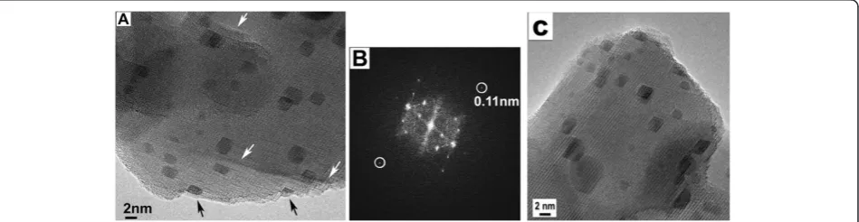
[image:3.595.64.539.572.695.2]Figure 2TEM-BF image, diffractogram, and movie clip. (A)TEM-BF image recorded at 600°C, showing the emerging Au on the surfaces (by black arrows) and the developing steps on Fe3O4(by white arrows);(B)diffractogram showing information transfer to 0.11 nm; and(C)movie clip constructed from the 1-s exposure still images.
Figure 1Bight-field transmission electron micrographs recorded in TEM mode. (A)Of leached Au/Fe2O3(hematite) catalyst at room temperature, showing voids and Au nanoparticles;(B)same support particle imaged at 500°C, revealing Au particle growth and void shrinkage;
black arrows. The information transfer from this image was calculated from the diffractogram of Figure 2B to be about 0.11 nm [21]. In Figure 2C, a movie clip is constructed from the TEM-BF images taken at 600°C that revealed the epitaxial growth of gold on iron oxide (Additional file 1).
STEM imaging results
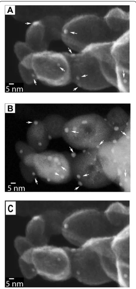
In Allard et al.’s earlier study of this materials system, whether the Au particles were on the surface or interior of the iron oxide support were deduced from the through-focus HAADF image series. The high resolution in Z (depth sectioning) in their study was made possible by the large probe incidence semiangle in the aberration-corrected in-strument [17]. It is a time-consuming approach which re-quired careful interpretation of a series of ADF images taken only from an aberration-corrected instrument. Unlike TE imaging, SE imaging has the advantage of being surface-sensitive and can thereby better reveal topographic informa-tion. Figure 3 presents a pair ofunprocessed, simultaneously acquired STEM-SE and STEM-ADF images taken at 500°C and 1.2 million times direct magnification. The SE image in Figure 3A reveals the Au particles as lighter-contrast dots (marked by white arrows), providing a better three-dimensional impression of the area than that of the ADF micrograph in Figure 3B. There are many more bright spots (Au) in Figure 3B, suggesting the extra spots are either within the iron oxide or on the bottom surfaces of the sup-port. The internal voids were revealed only in the ADF micrograph. Comparing the pair of images, the information from both surface and bulk are readily obtained. Movies of 30 frames/s were also recorded through the NTSC port pro-vided on the scanning control system. For instance, a movie clip in Figure 3C captures the structural change during heat-ing; the instant switching among SE, ADF, and BF signals provides a powerful means for studying dynamic processes that occurred on the surface and bulk of the catalyst (Additional file 2).
The spatial resolutions of Figure 3A,B were determined with the SMART-J method [22,23]. This method uses the Fourier transform (FT) of the image to separate the contribution of the signal (object) and the noise in the FT image. A resolution of 1.5 nm was determined for the SE image (Figure 3A), and a resolution of 1.6 nm was
determined for the ADF image (Figure 3B). The particle sizes were measured from intensity line scans extracted from the image. The size was defined by the full-width-half-maximum (FWHM) of the intensity peak correspond-ing to the particle. An average size of 3.3 ± 0.4 nm was obtained after the analysis of five particles. No difference in size was observed between the SE and ADF images.
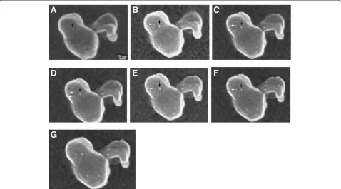
[image:4.595.306.538.88.579.2]Further heating at 700°C resulted in additional morpho-logical changes. Figure 4 shows a series ofunprocessedSE
Figure 3Simultaneous acquisition of a pair ofunprocessed
images taken at 700°C. Figure 4A shows a relatively smooth surface at the beginning of the 700°C heating cycle and the presence of a number of 1 nm Au particles. Figure 4B,C,D, E,F, acquired over 3 min, shows that the support surface developed terraces and facets and that some Au particles migrated on the terraces to coalesce into larger particles (e.g., as arrowed). A movie included in Figure 4G was con-structed from the still images (Additional file 3). A spatial resolution of 1.1 nm was determined with SMART-J method for all images in Figure 4. Heating of the specimen did not affect the resolution of the microscope, and although heating to 700°C caused the membrane to glow in the visible light range, no significant effect on the quality of the SE image was observed. This can be attributed to the tiny mass of the Aduro heating element, which does not emit enough photons to affect the electron detector, as opposed to the effect of light on secondary electron imaging when more standard heating stages employing bulk furnaces are used [1,2]. The size of the particle indi-cated by a black arrow was also measured on all images. An average size of 2.3 ± 0.3 nm was obtained. The size was not affected by heating, indicating it was isolated on the terrace of the iron oxide.
Secondary electron micrographs are formed using sec-ondary electrons (SE) and backscattered electrons (BSE). In
a recent study by Zhu et al. [24], conducted using an essen-tially identical secondary detector, the ratio of SE and BSE was found to be in the range of 85% to 90% (SE) to 15% to 10% (BSE) at 200 kV. We estimated the fraction of second-ary electrons exceeds 95% from a test using an atomically smooth silicon nitride film of 50-nm thick: the film facing the electron incident beam was clean. On the opposite side, we deposited Li3FePO4. There was absolutely no detectable contrast from the SE image. This test demon-strated that the signals from Figure 3A and Figure 4 are mostly from secondary electrons emitted from less than 50 nm depth. We further calculated that at 700°C the SE image resolution was 1.1 nm.
Conclusions
[image:5.595.59.538.90.355.2]In summary, we have demonstrated that 1.1-nm spatial resolution in secondary electron imaging can be achieved even during in situheating up to 700°C using a conven-tional TEM/STEM. We also have shown that information transfer in TEM imaging is about 0.14 nm at 600°C. Such a combined SEM and TEM in situ study is useful for nanomaterials research because information from the sur-face via SEM imaging and bulk via TEM/STEM imaging can be simultaneously obtained. If combined with simul-taneous nanoprobe spectroscopy (e.g., energy dispersive
from a series of SE images recorded at 300 kV at 700°C.
Competing interests
The authors declare that they have no competing interests.
Authors’contributions
JYH, LFA, and SHO came up with the research idea and wrote up the manuscript. JYH and LFA carried out experiments. WCB was responsible for the instrumentation. HD performed the SE imaging analysis and data interpretation. All authors read and approved the final manuscript.
Acknowledgements
Microscopy research at the Oak Ridge National Laboratory’s High Temperature Materials Laboratory was sponsored by the US Department of Energy, Office of Energy Efficiency and Renewable Energy, Vehicle Technologies Office, Propulsion Materials Program. This is a contributed paper and published as part of the Proceedings of the Microscopy and Microanalysis 2010, Portland, OR, USA, August, 2010.
Author details
1
Physical Sciences Directorate, Oak Ridge National Laboratory, 1 Bethel Valley Rd, TN 37831 Oak Ridge, USA.2Department of Materials Science and
Engineering, University of Michigan, 1221 Beal Avenue, Ann Arbor, MI 48104, USA.3Department of Mining and Materials Engineering, McGill University,
845 Rue Sherbrooke Ouest, Montreal, QC H3A 2B2, Canada.4Hitachi High-Technologies Canada Inc, 89 Galaxy Blvd, Toronto, ON M9W 6A4, Canada.
Received: 5 September 2014 Accepted: 3 November 2014 Published: 14 November 2014
References
1. Gregori G, Kleebe HJ, Siegelin F, Ziegler G:In situ SEM imaging at temperatures as high as 1450 degrees C.J Electron Microsc (Tokyo)2002, 51(6):347–352.
2. Seward GG, Prior DJ, Wheeler J, Celotto S, Halliday DJ, Paden RS, Tye MR: High-temperature electron backscatter diffraction and scanning electron microscopy imaging techniques: in-situ investigations of dynamic processes.Scanning2002,24(5):232–240.
3. Boyes ED, Gai PL:Environmental high-resolution electron microscopy and applications to chemical science.Ultramicroscopy1997,67:219–232. 4. Gai PL, Kourtakis K, Ziemecki S:In situreal-time environmental high
resolution electron microscopy of nanometer size novel xerogel catalysts for hydrogenation reactions in nylon 6,6.Microsc Microanal2000, 6(4):335–342.
5. Boyes ED:High resolutionin situSEM of competitive particle sintering and other surface processes.Microsc Microanal2002,8:408–409. 6. Williamson MJ, Tromp RM, Vereecken PM, Hull R, Ross FM:Dynamic
microscopy of nanoscale cluster growth at the solid-liquid interface.
Nat Mater2003,2:532–536.
7. Liu L:Advanced electron microscopy characterization of nanostructured heterogeneous catalysts.Microsc Microanal2004,10:55–76.
8. Gai PL, Boyes ED:Advances in atomic resolution in situ environmental transmission electron microscopy and 1A aberration corrected in situ electron microscopy.Microsc Res Tech2009,72(3):153–164.
A new MEMS-based system for ultra-high-resolution imaging at elevated temperatures.Micros Res Tech2009,72:208–215.
16. Allard LF, Borisevich A, Deng W, Si R, Flytzani-Stephanopoulos M, Overbury SH:Evolution of gold structure during thermal treatment of Au/FeOx
catalysts revealed by aberration-corrected electron microscopy.J Electron Microsc2009,58:199–212.
17. Allard LF, Flytzani-Stephanopoulos M, Overbury SH:Behavior of Au species in Au/FeOxcatalysts as a result ofin situthermal treatments, characterized via
aberration-corrected STEM imaging.Microsc Microanal2010,16:375–385. 18. Howe JY, Allard LF, Bigelow BC, Overbury SH:Synergy of combined (S)TEM
imaging techniques for the characterization of catalyst behavior during in situheating.Microsc iMicroanal2010,16(S2):312–313.
19. Shive PN, Diehl J:Reduction of hematite to magnetite under natural and laboratory conditions.J Geomagn Geoelectr1977,29:345–354.
20. Absalyamov SS, Mulyukov KY:The stability of hematite in small-size particles.Dokl Phys2000,45:657–658.
21. Russ JC:The image processing handbook 6th edn.Boca Raton: CRC Press; 2011. 22. Joy DC:SMART - a program to measure SEM resolution and imaging
performance.J Microsc Oxford2002,208:24–34.
23. Kim J, Jalhadi K, Lee SY, Joy DC:Fabrication of a Fresnel zone plate through electron beam lithographic process and its application to measuring of critical dimension scanning electron microscope performance.J Vac Sci Technol B2007,25:1771–1775.
24. Zhu Y, Inada H, Nakamura K, Wall J:Imaging single atoms using secondary electrons with an aberration-corrected electron microscope.Nat Mater
2009,8:808–812.
doi:10.1186/1556-276X-9-614
Cite this article as:Howeet al.:Understanding catalyst behavior during
in situheating through simultaneous secondary and transmitted
electron imaging.Nanoscale Research Letters20149:614.
Submit your manuscript to a
journal and benefi t from:
7Convenient online submission
7Rigorous peer review
7Immediate publication on acceptance
7Open access: articles freely available online
7High visibility within the fi eld
7Retaining the copyright to your article