N A N O E X P R E S S
Open Access
Formation of Self-Connected Si
0.8
Ge
0.2
Lateral Nanowires and Pyramids on
Rib-Patterned Si(1 1 10) Substrate
Lei Du, Gang Chen
*and Wei Lu
Abstract
In this work, Si0.8Ge0.2is deposited onto the rib-patterned Si (1 1 10) template oriented in the [1−1 0] direction. Atomic force microscopy (AFM) reveals that the rib sidewalls reshape into pyramid-covered (0 0 1) and smooth {1 1 3} facets, respectively, while the {1 0 5} facets-bounded lateral SiGe nanowires dominate the rib top along the [5 5−1] direction. At both the rib shoulder sites and the pyramid vacancy sites, self-connecting occurs between the meeting nanowire and pyramids to form elongated huts, which are driven by the minimization of the total energy density according to the finite-element simulations results. These results suggest a convenient solution to form lateral SiGe nanowires covering multi-faceted surfaces on the patterned template.
Keywords:Germanium, Lateral nanowires, Finite-element simulation, Patterned template, Molecular beam epitaxy
Background
As an alternative candidate for the miniaturized comple-mentary metal oxide semiconductor field effect transis-tors (MOSFET) [1–3], and many other promising applications [4–6], Ge-based nanowires have been exten-sively studied owing to their compatibility with the well-established Si-based semiconductor technology. So far, the bottom-up vapor-liquid-solid (VLS) growth method has been successfully developed and applied to fabricate Ge and Ge/Si core/shell nanowires with excellent device performance [4, 7]. Nevertheless, there has not been any convenient solution available to transfer/arrange these vertically grown nanowires yet, which limits its potential application in microelectronics [6]. On the other hand, recently laterally aligned heteroepitaxial in-plane Ge nanowires on Si substrate have been regarded as an al-ternative solution on both singular [8–12] and miscut [13, 14] Si (0 0 1) and Si (1 1 1) [15, 16] substrates, espe-cially the Si (1 1 10) surface [17–19], where the lateral nanowires can naturally extend along the [5 5−1] direc-tion. The mechanism behind the formation and stability of these nanowires are attributed to abnormal faceting
of the wetting layer [6, 13] or extended huts [10, 20], which is driven by the low surface energy of their {1 0 5} side facets under equilibrium phase. These lateral wires have shown potential applications for nano-electronics [10, 21], spintronic devices [22, 23], and optoelectronics [24, 25].
To further explore the excellent features of SiGe lat-eral nanowires, it becomes necessary to fully understand the mechanism of the nanowire formation on various substrates for the steerable growth. So far, template pat-terning is one of the most successful routes to achieve controllable growth of the lateral SiGe nanowires on both miscut [19] and singular Si (001) substrate [26]. Re-cent work has also showed the morphology evolution between the nanowires and the islands during the vari-ation of the growth temperature and the thickness of the Si spacer [27, 28]. Nevertheless, there has been very few reports on the evolution of the SiGe lateral nanowires on the patterned miscut substrate, where the coexistence of the nanowires and islands are inevitable. It is neces-sary to study the controlled growth of SiGe nanowires on patterned templates, while the interaction between the nanowires and the islands on multi-faceted template, and especially at the shoulders or connecting edges, also has to be investigated.
* Correspondence:[email protected]
National Laboratory for Infrared Physics, Shanghai Institute of Technical Physics, Chinese Academy of Sciences, 500 Yutian Road, Shanghai 200083, China
Therefore, here we apply a different strategy for the template patterning from what have been used before. In our previous work, the ribs are patterned onto the Si (1 1 10) substrate along the [5 5 −1] direction to ensure the formation of micromillimeter-long nanowires via the geometry-induced self-elongation and self-alignment effects [19]. On the other hand, in this work, the ribs are patterned along the [1−1 0] orientation which is perpen-dicular to the expected SiGe nanowire direction. Since the SiGe nanowires self-align along the [5 5 −1] direction, such a configuration will truncate the nanowires at the shoulder of the ribs [29]. With a well-tuned lithography technique and the buffer layer growth conditions, the (001) faceted sidewalls are introduced adjacent to the (1 1 10) terminated rib top. Thus, we can study the interactions between the nanowires and other self-assembled nano-structures on two adjacent facets.
As for the choice of the SiGe concentration, we fo-cused on the Si0.8Ge0.2 nanowires in this work due to the promising features both in thermal transport [30] and carrier transport [31] for Si-rich Si1-xGex hetero-structures (especially when x= 0.2), which recently have been intensively explored for potential thermoelectronic applications [32, 33], and for achieving semiconductor quantum dot spin qubit [34–36].
Thus, we studied the behavior of the formation of the nanowires and islands by Si0.8Ge0.2heteroepitaxy on rib-patterned Si (1 1 10) substrates in this work. Total en-ergy density studies via finite-element methods (FEM) were also carried out for discussion on the possible evo-lution routes on the patterned substrate and their under-lying driven forces.
Methods
9 × 9 mm2pieces of Si (1 1 10) substrates were patterned with a Leo Supra 35 field emission scanning electron microscope (FE-SEM) and subsequent reactive ion etch-ing in an Oxford Plasmalab 80 reactor into 200 × 200 μm2 large arrays of parallel ribs along the [1 −1 0] direction. And the periodicities range from 0.5 to 2.5μm, with the bottom width of the ribs ranging from 0.4 to 2.4 μm. The samples were chemically pre-cleaned using the RCA method. Immediately after a final hydro-fluoric acid treatment, the samples were loaded into Riber® SIVA45 system for the molecular beam epitaxy (MBE) growth. After an in situ thermal desorption step at 950 °C for 10 min, a 30-nm-thick Si buffer layer was de-posited while ramping the substrate temperature from 450 to 520 °C. Subsequently, 150 monolayers (ML) of Si0.8Ge0.2were deposited at 650 °C with a rate of 0.12 Å/s. This thickness has been selected based on the successful formation of SiGe nanowires on both singular Si (1 1 10) [19] and patterned Si (0 0 1) [26] substrates without intro-duction of defects. As in previous work, the surface
morphologies were characterized via ex situ atomic force microscopy (AFM) using a Veeco® Dimension 3100 system in the tapping mode. The AFM images were processed with the Gwyddion® analysis package. The experimental geometry was used for finite-element method (FEM) cal-culations of the total energy density. Modeling based on the experimentally observed geometry was performed by a FEM analysis of the Ge nanowires with the commercial COMSOL Multiphysics® 4.3 package.
Results and Discussion
Figure 1a shows the derivative view of a 5 × 5μm2AFM image for a reference sample after the growth of 150 ML Si0.8Ge0.2 on a flat Si (1 1 10) substrate at 650 °C. The {105} faceted ripples dominated the whole surface, as can be seen in the surface orientation map (SOM; lower left inset). They are oriented along the [5 5−1] direction, with the average ripple width of 140 ± 20 nm via 2D Fourier transform analysis (not shown here). The surface morphology of a typical rib-patterned Si (1 1 10) tem-plate used in this work is shown in Fig. 1b with a three dimensional (3D) rendering of the AFM image for an area of 2 × 2 μm2 and with the ribs’ orientation aligned along [1−1 0] as a lower right inset in Fig. 1a. The peri-odicity of the ribs is about 500 nm, and the top width of the ribs is about 200 nm.
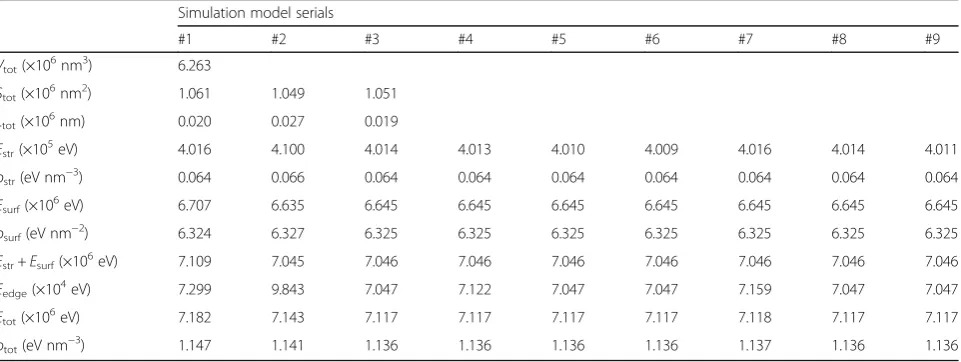
Figure 2a, c are the top view and the 3D rendering of a 5 × 2.5 μm2 AFM image for the patterned Si (1 1 10) templates with the rib-top width of 450 nm after growth of 150 ML Si0.8Ge0.2 at 650 °C. And Fig. 2b is the
[image:2.595.306.538.461.684.2]sectional profiles measured along the dashed guiding lines in Fig. 2a. Figure 2d is the SOM which helps to de-termine the faceting of the surface morphology. The AFM images show the top of the ribs has already been dominated by the {105} facet-bounded SiGe nanowires labeled as “A” with the width of about 200 nm as con-firmed by SOM in Fig. 2d. The ribs are connecting two neighboring sidewalls, one of which is fully decorated with SiGe pyramid-shaped islands (labeled as “C” in Fig. 2a–c) featured with {105} facets as well according to the SOM. The symmetric geometry of the pyramids indicates that the sidewall they are sitting on has been faceted into an (0 0 1) surface. The opposites sidewall of the ribs are rather smooth with an inclination angle α= 17 ± 0.5° measured from the profile in Fig. 2b, which can be attributed to the {113} facets by SOM in Fig. 2d as well. This sidewall connects to the valley between the neighboring ribs, where short nanowires have also formed and have been labeled as “B” with an average width of about 200 nm. Nevertheless, these nanowires are terminated with dome-like {15 3 23} facets and {1 1 3} facets as indicated by the inclination map of two nanowires in the inset of Fig. 2c, and the SOM in Fig. 2d confirms these observations. With the bottom width increased up to 1.5μm, the morphology of the rib top develops into the {105} facet-bounded nano-wires as well, as shown in Fig. 2e, f. The length of these
[image:3.595.56.291.87.336.2]nanowires are limited by the width of the rib top, which is about 200 ± 50 nm as indicated in Fig. 2f. Be-sides the islands, short huts along the [100] direction can also be observed as pointed with white arrows in Fig. 2e. With the bottom width of the rib increasing up to 1.6 ± 0.1 μm, the rib top is fully covered by nanowires with the length of about 1.1 ± 0.1 μm as can be seen in Fig. 2g, h.
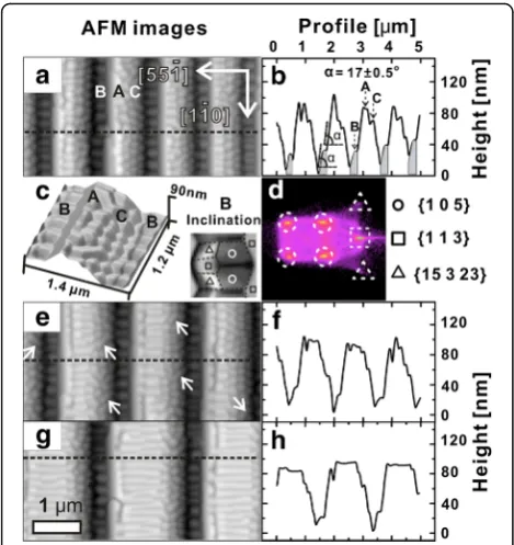
Figure 3a shows a Laplacian-filtered AFM image for the sample with the rib bottom width of about 1.6μm to highlight the surface morphology, especially the faceting. It is well resolved that most of the nanowires on the rib top are terminated with two intersecting {105} facets [27]. Moreover, a self-connecting phenomenon at the rib shoulder between the nanowires on rib-top and the pyr-amids on the (0 0 1) faceted sidewall has been observed as highlighted with dashed circles in Fig. 3a. A zoom-in view of the AFM image in the down-right inset of Fig. 3a reveals that self-connecting is achieved through the fill-ing of the vacancies between the neighborfill-ing nanowires and the pyramids with ad-atoms, which enables the mer-ging of the two opposite {105} facets of the nanowires seamlessly to form extended nanowires on both the rib-top and the (0 0 1) faceted sidewall. Figure 3b is a 3D schematic for an idealized sample morphology with the whole Si (001) facet fully packed by pyramids, which is also the base for further finite-element simulation study. The diagonal of the pyramids is the same as the width of the nanowires on the rib-top of 200 nm, based on the AFM measurement. To form the extended nanowires, a tetrahedron section highlighted with red lines between for the nanowire and the pyramid is to be filled as shown in Fig. 3b. Figure 3c is the top view of the sche-matic where the two smoothly self-connected {105} facets of extended nanowires are marked with shadows to indicate the final surface morphology. While the co-existence of SiGe huts with the pyramids on both flat Si (001) and Si (1 1 10) substrates has been observed and studied systematically [26, 27], the self-connecting of the nanowires with the pyramids at the rib shoulder between the (1 1 10) rib-top and the (0 0 1) faceted sidewall has not been reported yet. Many huts can be observed sit-ting on the faceted sidewalls at various sites in the AFM images as highlighted by square dashes shown in Fig. 3a, although they are missing in Fig. 3b to simplify the model based on the observation that they are not ob-servable overall, as Fig. 3a suggests. Meanwhile, we also find the absence of the self-connecting phenomenon at the bottom of the sidewall connecting to the {1 1 3} facet as highlighted by the yellow dashed rectangle in Fig. 3a.
The profile of the model with the information on the faceting and concentration of the materials is shown in Fig. 3d. The model itself is constructed based on the AFM results of the sample shown in Fig. 3a. A 100-nm-Fig. 2a,c,e 5 × 2.5μm2 AFM images for the rib-patterned Si
(1 1 10) templates with the top width of 450, 800, and 1100 nm after growth of 150 ML Si0.8Ge0.2at 600 °C.b,d,f
The cross-sectional profiles measured along the corresponding
thick Si is chosen as the template. The rib is 56 nm in height, with a 25-nm-thick Si0.8Ge0.2 wetting layer shell painted in violet in Fig. 3d and a Si substrate core. The width of the Si0.8Ge0.2 nanowires is 200 nm, and thus, they are 14 nm in height, based on the AFM measure-ment as well. The width of the pyramids is fixed as the same value of the nanowires, i.e., 200 nm. The position and the orientation of the {113} faceted sidewall and the pyramid-covered (0 0 1) sidewall are also highlighted with a red solid line and green dashed line, respectively.
In this work, the rib-patterned template provides geometric condition to achieve the coexistence of both (1 1 10) faceted rib top and the (0 0 1) faceted sidewall. This leads to the simultaneous formation of nanowires on the rib top and the packed pyramids on the sidewall. Moreover, the onset of the self-connections between the nanowires and the pyramids at the rib shoulder and be-tween the pyramids on the sidewall has also been ob-served. These results raise the question whether the self-connecting occurs at any preferential site, e.g., at the rib shoulder or at a rather random site without preference. The other question is: what is the driving force for the self-connecting of the nanowire-pyramid and pyramid-pyramid pairs? That is, is there any other energetically favorite way to distribute the volume of the tetrahedron
with the concentration of the deposited materials being fixed. To answer these two questions, total energy density study for the deposited system including the nanowires and the pyramids using FEM calculations were carried out. The total energy density ρtot is given by ρtot= (Estr+Esurf+Eedge) /Vtot, where Estr, Esurf, and
[image:4.595.59.539.88.391.2]observed in previous studies [9, 14, 39]. This means that the trend of the surface energy with strain is implemented in the model and the effective value of the surface energy is computed by taking into account the real strain on these facets. Finally, the edge energy termEedgeis given by
Eedge=ρedge×L, where ρedge is the energy density of the top and two basal ripple facet intersections, andL is the length of the nanowire. In our calculation,ρedge= 3.7 eV/ nm is adopted for the {105}/{105} edge as well as the pro-posed (1 1 10)/{1 0 5} and (0 0 1)/{1 0 5} edges [17]. Dur-ing the calculation, periodic boundary conditions are applied to both [5 5−1] and [1−1 0] directions. Thus, the region in the pink dashed line in Fig. 3d is used to perform the FEM simulation.
As an indication for the experimental origin of the proposed models, Fig. 4a is a section of the rotated 3D rendering of the AFM image in Fig. 3a. The black arrow
indicates a self-connecting between the nanowire and the pyramid at the rib shoulder. Figure 4b–j shows the final improved models for the calculation with the self-connecting effect on the sidewall being taken into con-sideration. The major strategy is to compare the total energy density of the various models created by the dis-tribution of the fixed amount of Si0.8Ge0.2materials onto the basic model dominated by the combination of nano-wires and pyramids on the rib-patterned template as shown in Fig. 3b with different configurations. The vol-ume of the distributed Si0.8Ge0.2materials is equal to the volume of two tetrahedron sections. Figure 4b, c shows models #1 and #2 representing the two alternative con-figurations, respectively. In Fig. 4b, the distributed ad-atoms accumulate at the valleys in between the adjacent nanowires and the pyramids to fill the bottom of the concave valleys as a kinetic-driven behavior [40]. In
[image:5.595.58.538.308.695.2]Fig. 4c, the size of a single specific pyramid is increased with the accumulation of the additional SiGe materials as highlighted with blue. The rest of the models, i.e., models #3, #4, #5, #6, #7, #8, and #9 with different con-figurations of the tetrahedrons connecting the pyramids, are proposed partly based on the experimental observa-tions and are shown in Fig. 4d–j, respectively. Indeed, model #7 shown in Fig. 4h has not been observed in AFM images. And we also input this model into the cal-culation to investigate the reason for the absence of this configuration. In all these models, two tetrahedron sec-tions are inserted to fill the vacancies between the adja-cent nanowire/pyramid or pyramid/pyramid pairs to simulate the self-connecting phenomenon. In Fig. 4d, two huts are formed with two separate nanowire/pyra-mid pairs. In Fig. 4e, the situation that one nanowire is connecting to two separate pyramids simultaneously is considered. Models in Fig. 4f, g are used to simulate the cases that the self-connecting occurs between the neigh-boring pyramids at different sites on the Si (001) faceted sidewall. Then in Fig. 4h, the two tetrahedron sections are inserted to form the two separate huts connecting the nanowires sitting at the bottom of the rib valley and the pyramids at the sidewall. Elongated self-connecting is also taken into consideration with the models in Fig. 4i, j by aligning the two tetrahedron sections in a line. With these models, the typical configuration for the self-connecting observed are all represented. The 3D view and the cross-sectional view for the calculated strain en-ergy distribution for the nanowires and pyramids in model #3 are shown in Fig. 4k, l.
All the above models are then input into FEM simula-tion. The calculated results are exhibited in Table 1. The total volumeVtotfor the nanowires and the pyramids for all these models is determined to be 6.2632 × 10⁶ nm3. The total surface areaStotfor model #1 is 1.061 × 10⁶nm2, and for model #2 1.049 × 10⁶nm2. For model #1, the size
expansion of the center pyramid leads to the increasing of the exposed area. For model #2, the flattening of the bot-tom of the valleys with (0 0 1) and (1 1 10) facets for the pyramids and nanowires cause the reduction of the total exposed area. The remaining seven models have the same value of the surface area of 1.051 × 10⁶nm2due to the fact that they share similar geometry with different sites for the inserted tetrahedrons. The total edge length Ltot of model #1 is slightly larger than the rest of the models due to the increase of the volume of the center pyramid by about 5%. On the other hand, the flattening of the valley bottom leads to the introduction of additional edges, thus significantly increasing the total edge length by 42%. Fur-ther results show that the calculated strain energy density ρstrand the surface energy densityρsurffor all the models are almost of the same value 0.064 ± 0.002 eV nm−3 and 6.325 ± 0.002 eV nm−2, respectively. So the calculated sum of the surface energy and the strain energyEstr+ Esurf for model #1 is about 7.109 × 10⁶ eV, which is about 0.9% larger than all the rest of the models. Then, we take the edge energy into consideration. As can be seen in Table 1, the edge energy for model #2 is 9.843 × 10⁴ eV, which is about 35~40% higher than all the other models. This is due to the fact that in model #2, additional (1 1 10)/{1 0 5} and (0 0 1)/{1 0 5} edges are introduced during the flattening of the val-ley bottom. And in the other models, the filling of the vacancies with tetrahedrons can replace the four pyramid edges with one top edge, which effectively reduces the edge energy for the whole system.
[image:6.595.59.540.551.732.2]Thus, the total energy and the total energy density can be obtained. These results show that the total energy density for both models #1 and #2 are 1.147 and 1.141, which are about 1 and 0.4% higher than the rest models, respectively. For model #1, the higher surface area, and thus the higher surface energy, contributes to the higher total energy. This phenomenon has been observed
Table 1The calculated results with FEM for the nine proposed models with different configurations of surface morphology
Simulation model serials
#1 #2 #3 #4 #5 #6 #7 #8 #9
Vtot(×106nm3) 6.263
Stot(×106nm2) 1.061 1.049 1.051
Ltot(×106nm) 0.020 0.027 0.019
Estr(×105eV) 4.016 4.100 4.014 4.013 4.010 4.009 4.016 4.014 4.011
ρstr(eV nm− 3
) 0.064 0.066 0.064 0.064 0.064 0.064 0.064 0.064 0.064
Esurf(×106eV) 6.707 6.635 6.645 6.645 6.645 6.645 6.645 6.645 6.645
ρsurf(eV nm− 2
) 6.324 6.327 6.325 6.325 6.325 6.325 6.325 6.325 6.325
Estr+ Esurf(×106eV) 7.109 7.045 7.046 7.046 7.046 7.046 7.046 7.046 7.046
Eedge(×104eV) 7.299 9.843 7.047 7.122 7.047 7.047 7.159 7.047 7.047
Etot(×106eV) 7.182 7.143 7.117 7.117 7.117 7.117 7.118 7.117 7.117
ρtot(eV nm− 3
before during the synchrotron radiation-based grazing incidence small angle X-ray scattering measurement [41], in which the stabilization of the prism structure is attributed to the strain-dependence of the {105} surface energy. And our FEM results seem to support this in terms of total energy density analysis. As for model #2, although the edge energy only takes up about 1% of the total energy, the much higher edge energy still plays a key role in the comparison of total energy as discussed before [17], which rules out the possibility to form the enlarged pyramids on the patterned substrate. The total energy density difference exhibited above is quite small. Nevertheless, this is not uncommon that a small total energy difference in the order of 1% may lead to the onset of the energetically preferential geometry [19, 27], so long as the quasi equilibrium growth condition is fulfilled. The rather low deposition rate of 0.12 Å/s and medium temperature of 650 °C during our MBE growth exactly provide the favorite condition which enabled the thermodynamics the dominating driven force for the observed phenomena.
The rest of the configurations all behold almost identical total energy density of 1.136 eV/nm3no matter where the inserted tetrahedrons are, with the exception of model #7 that has the value of 1.137 eV/nm3. This result fits the fact that all the above configurations, except #7 with only about 0.88‰larger in the total energy density, have been experimentally observed. It is again the difference in the edge energy that counts for these results. The same value of the total energy density for configurations #3, #4, #5, #6, #8, and #9 indicates the self-connecting can onset at any vacancies to form hut-like structures without energet-ically preferential site, once the (0 0 1) faceting is achieved during the SiGe epitaxy [42].
FEM results provide possible explanations for the ex-perimentally observed phenomena in terms of energetic comparison. The driving force for the onset of the self-connecting instead of all competing configurations is at-tributed to the minimization of the total energy density. And all the components of the total energy, including the minimal edge energy term, contribute to the deter-mination of the final morphology.
It should be noted that the formation of the nanowires on (1 1 10) faceted rib top and the pyramids and the elongated huts on (0 0 1) faceted sidewall are mainly two separate processes. Early work shows the formation of pyramids on Si (001) substrate after deposition of 3.8 nm Si0.7Ge0.3 [43]. With similar coverage of 30 ML, Si0.8Ge0.2 nanowires formation also onsets on Si (1 1 10) substrate [41]. Thus, due to the rather low growth rate and medium growth temperature used in our work, it can be expected that the nanowires and the pyramids form simultaneously on both facets. Further geometry evolution for the Si-rich SiGe on flat Si(1 1 10) substrate
has also been elaborated in previous work [27, 41]. But in this work, the rib-patterning along the [1−1 0] direction induces the truncating for nanowires at the rib shoulders. Therefore, we observed that most of the nanowires on the rib top are terminated with two intersecting {105} facets, as shown and discussed in Fig. 3a, which coincides with the “tadpole” configuration onsets during the geometric evolution from 1D nanowire towards 3D island [27]. Since this configuration were evolved from the (0 0 1) termi-nated ripple, it is reasonable to suppose the nanowire ends terminated with intersecting {105} facets on the rib shoul-der also developed from (0 0 1) faceted termination during the growth. On the other hand, ab initio calculations show the potential fluctuations on reconstructed Ge {105} sur-face are very small [44], and the sursur-face migration of SiGe ad-particles on it is fast and almost isotropic, which can significantly enhance the interaction between the nano-wires on the rib top and the pyramids on the (0 0 1) side-wall. Indeed, the observed width of the nanowires and length of pyramid diagonal finally evolved into the same value of about 200 nm. Thus, at the shoulder sites, the nanowires and the pyramids generally self-arranged into the close packing configuration, with each nanowire wedging in between two neighboring pyramids, as ob-served in Fig. 3a and schematically illustrated in Fig. 3b, c. The well-developed geometry at the rib shoulder paves the evolution route for further connecting between the nanowires on (1 1 10) faceted rib top and the pyramids/ elongated huts on (0 0 1) faceted sidewall.
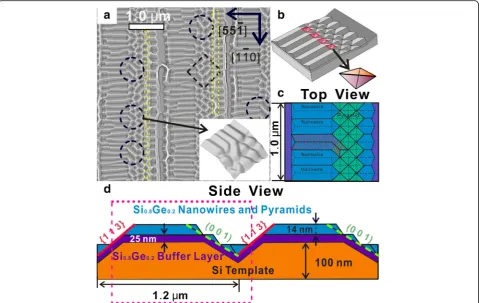
On the other hand, the formation the elongated huts through the self-connecting between the pyramids is indeed the precursor before the final formation of the Si-rich SiGe nanowires on Si (0 0 1) substrate [26, 42, 45]. Once the self-connecting can be achieved at the shoulder site, the long SiGe nanowire with random direction along orthogonal [0 −1 0] directions covering both the rib top and the sidewall as shown in Fig. 5a can be expected with increasing coverage and moderate annealing. However, to achieve a completely aligned nanowire array fully covering both connected facets as shown in Fig. 5b, alternative growth method with well-tuned growth condition [10]
[image:7.595.307.538.597.694.2]based on the thermodynamic wave model [17] and the additional geometric restrictions [26] have to be applied.
Conclusions
In conclusion, heteroepitaxy of Si0.8Ge0.2 onto rib-patterned Si (1 1 10) templates oriented along [1 −1 0] leads to the formation of SiGe nanowires on the rib top along [5 5 −1] direction, as well as the sidewalls bound with respective (0 0 1) and (1 1 3) facets. While the (1 1 3) dominated sidewalls keep smooth, the (0 0 1) faceted side-walls are fully decorated with closely packed SiGe pyra-mids and huts. Finite-element simulations reveal that the formation of the huts on Si (001) via the self-connecting of the adjacent pyramids, as well as between the nano-wires and the pyramids at the rib shoulder sites are both driven by the minimization of the total energy density, while the competing geometric evolution routes via pyra-mid expansion and valley flattening are suppressed. These results provide a convenient solution to fabricate the self-assembled in-plane nanowires covering multi-faceted sur-faces on the patterned templates.
Abbreviations
3D:Three dimension; AFM: Atomic force microscopy; FEM: Finite-element methods; FE-SEM: Field emission scanning electron microscope;
MBE: Molecular beam epitaxy; ML: Monolayer; SOM: Surface orientation map; VLS: Vapor-liquid-solid
Acknowledgements
This work is supported by Chinese Academy of Sciences via Hundred Talents Program and the National Natural Science Foundation of China via No.61474130. We also thank Daniele Scopece for the insightful discussion and proofreading.
Authors’Contributions
The idea of this study was conceived by GC. GC mainly took part in the SiGe heteroepitaxy growth and AFM measurement, preparing Figs. 1, 2, 3, 4, and 5. LD carried out the simulations via finite-element methods, preparing Figs. 3 and 4 and Table 1. WL, GC and LD interpreted the calculation results and completed the manuscript. All authors wrote and reviewed this manuscript. All authors read and approved the final manuscript.
Competing interests
The authors declare that they have no competing interests.
Received: 3 November 2016 Accepted: 26 December 2016
References
1. Morales AM, Lieber CM (1998) A laser ablation method for the synthesis of crystalline semiconductor nanowires. Science 279:208–211
2. Kodambaka S, Tersoff J, Reuter MC, Ross FM (2007) Germanium nanowire growth below the eutectic temperature. Science 316:729–732 3. Xiang J, Lu W, Hu YJ, Wu Y, Yan H, Lieber CM (2006) Ge/Si nanowire
heterostructures as high-performance field-effect transistors. Nature 441: 489–493
4. Duan XF, Huang Y, Agarwal R, Lieber CM (2003) Single-nanowire electrically driven lasers. Nature 421:241–245
5. Lu W, Xiang J, Timko BP, Wu Y, Lieber CM (2005) One-dimensional hole gas in germanium/silicon nanowire heterostructures. Proc Natl Acad Sci USA 102:10046–10051
6. Chan CK, Zhang XF, Cui Y (2008) High capacity Li ion battery anodes using Ge nanowires. Nano Lett 8:307–309
7. Wu YY, Yang PD (2000) Germanium nanowire growth via simple vapor transport. Chem Mater 12:605–607
8. Ohmori K, Foo YL, Hong S, Wen JG, Greene JE, Petrov I (2005) Directed self-assembly of Ge nanostructures on very high index, highly anisotropic Si(hkl) surfaces. Nano Lett 5:369–372
9. Persichetti L, Sgarlata A, Fanfoni M, Balzarotti A (2010) Shaping Ge islands on Si(001) surfaces with misorientation angle. Phys Rev Lett 104:036104 10. Zhang JJ, Katsaros G, Montalenti F, Scopece D, Rezaev RO, Mickel C,
Rellinghaus B, Miglio L, De Franceschi S, Rastelli A, Schmidt OG (2012) Monolithic growth of ultrathin Ge nanowires on Si(001). Phys Rev Lett 109: 085502
11. Bansen R, Schmidtbauer J, Gurke R, Teubner T, Heimburger R, Boeck T (2013) Ge in-plane nanowires grown by MBE: influence of surface treatment. CrystEngComm 15:3478–3483
12. Alonso MI, Bailo E, Garriga M, Molero A, Vaccaro PO, Goñi AR, Ruiz A, Alonso M (2015) Composition and strain imaging of epitaxial in-plane SiGe alloy nanowires by micro-Raman spectroscopy. J Phys Chem C 119:22154–22163 13. Zhou T, Vastola G, Zhang YW, Ren Q, Fan Y, Zhong Z (2015) Unique features
of laterally aligned GeSi nanowires self-assembled on the vicinal Si (001) surface misoriented toward the [100] direction. Nanoscale 7:5835–5842 14. Berbezier I, Ronda A (2007) Self-assembling of Ge dots on nanopatterns:
experimental investigation of their formation, evolution and control. Phys Rev B 75:195407
15. Zhu JH, Brunner K, Abstreiter G, Kienzle O, Ernst F, Ruhle M (1999) Correlated SiGe wires shaped by regular step bunches on miscut Si(113) substrates. Phys Rev B 6:10935–10940
16. Shklyaev AA, Latyshev AV (2016) Formation of lateral nanowires by Ge deposition on Si(111) at high temperatures. J Crystal Growth 441:84–88 17. Chen G, Sanduijav B, Matei D, Springholz G, Scopece D, Beck MJ, Montalenti F,
Miglio L (2012) Formation of Ge nanoripples on vicinal Si (1110): from Stranski-Krastanow seeds to a perfectly faceted wetting layer. Phys Rev Lett 108:055503 18. Zhong ZY, Gong H, Ma YJ, Fan YL, Jiang ZM (2011) A promising routine to
fabricate GeSi nanowires via self-assembly on miscut Si (001) substrates. Nanoscale Res Lett 6:322
19. Du L, Scopece D, Springholz G, Schäffler F, Chen G (2014) Self-assembled in-plane Ge nanowires on rib-patterned Si (1110) templates. Phys Rev B 90:075308 20. Daruka I, Grossauer C, Springholz G, Tersoff J (2014) Equilibrium phase
diagrams for the elongation of epitaxial quantum dots into hut-shaped clusters and quantum wires. Phys Rev B 89:235427
21. Maier F, Klinovaja J, Loss D (2014) Majorana fermions in Ge/Si hole nanowires. Phys Rev B 90:195421
22. Pan JZ, Zhou T, Jiang ZM, Zhong ZY (2013) Anomalous magnetoresistance of an array of GeSi nanowires. Appl Phys Lett 102:183108
23. Maier F, Kloeffel C, Loss D (2013) Tunable g factor and phonon-mediated hole spin relaxation in Ge/Si nanowire quantum dots. Phys Rev B 87:161305 24. Scopece D, Montalenti F, Bonera E, Bollani M, Chrastina D (2014) Straining
Ge bulk and nanomembranes for optoelectronic applications: a systematic numerical analysis. Semicond Sci Technol 29:095012
25. Zhou T, Zhong ZY (2014) Dramatically enhanced self-assembly of GeSi quantum dots with superior photoluminescence induced by the substrate misorientation. APL Mat 2:022108
26. Chen G, Springholz G, Jantsch W, Schaffler F (2011) Self-aligned fabrication of in-plane SiGe nanowires on rib-patterned Si (001) substrates. Appl Phys Lett 99:043103
27. Sanduijav B, Scopece D, Matei D, Chen G, Schaffler F, Miglio L, Springholz G (2012) One-dimensional to three-dimensional ripple-to-dome transition for SiGe on vicinal Si (1 1 10). Phys Rev Lett 109:025505
28. Zhang JJ, Schmidt OG (2013) Strain-induced self-assembly of Ge nanodashes, nanodumbbells, and dot chains on Si(001). Appl Phys Lett 103:143112 29. Chen G, Vastola G, Zhang JJ, Sanduijav B, Springholz G, Jantsch W, Schaffler F
(2011) Enhanced intermixing in Ge nanoprisms on groove-patterned Si(1 1 10) substrates. Appl Phys Lett 98:023104
30. Vining CB, Laskow W, Hanson JO, Van der Beck RR, Gorsuch PD (1991) Thermoelectric properties of pressure-sintered Si0.8Ge0.2thermoelectric
alloys. J Appl Phys 69:4333
31. Lu TM, Tsui DC, Lee CH, Liu CW (2009) Observation of two-dimensional electron gas in a Si quantum well with mobility of 1.6 × 106cm2/Vs. Appl
Phys Lett 94:182102
32. Xu B, Li CB, Thielemans K, Myronov M, Fobelets K (2012) Thermoelectric performance of Si0.8Ge0.2nanowire arrays. IEEE T Electron Dev 59:3193
34. Kim D, Shi Z, Simmons CB, Ward DR, Prance JR, Koh TS, Gamble JK, Savage DE, Lagally MG, Friesen M, Coppersmith SN, Eriksson MA (2014) Quantum control and process tomography of a semiconductor quantum dot hybrid qubit. Nature 511:70
35. Eng K, Ladd TD, Smith A, Borselli MG, Kiselev AA, Fong BH, Holabird KS, Hazard TM, Huang B, Deelman PW, Milosavljevic I, Schmitz AE, Ross RS, Gyure MF, Hunter AT (2015) Isotopically enhanced triple-quantum-dot qubit. Sci Adv 1, e1500214
36. Lu TM, Gamble JK, Muller RP, Nielsen E, Bethke D, Ten Eyck GA, Pluym T, Wendt JR, Dominguez J, Lilly MP, Carroll MS, Wanke MC (2016) Fabrication of quantum dots in undoped Si/Si0.8Ge0.2 heterostructures using a single metal-gate layer. Appl Phys Lett 109:093102
37. Cereda S, Montalenti F, Miglio L (2005) Atomistic modeling of step formation and step bunching at the Ge(105) surface. Surf Sci 591:23–31 38. Scopece D, Beck MJ (2013) Epilayer thickness and strain dependence of
Ge(113) surface energies. Phys Rev B 87:155310
39. Jernigan GG, Thompson PE, Silvestre CL (1997) Quantitative measurements of Ge surface segregation during SiGe alloy growth. Surf Sci 380:417 40. Myslivecek J, Schelling C, Schaffler F, Springholz G, Smilauer P, Krug J,
Voigtländer B (2002) On the microscopic origin of the kinetic step bunching instability on vicinal Si(001). Surf Sci 520:193–206
41. Chen G, Wintersberger E, Vastola G, Groiss H, Stangl J, Jantsch W, Schaeffler F (2010) Self-assembled Si0.80Ge0.20nanoripples on Si (1 1 10) substrates. Appl
Phys Lett 96:103107
42. Gray JL, Hull R, Lam CH, Sutter P, Means J, Floro JA (2005) Beyond the heteroepitaxial quantum dot: Self-assembling complex nanostructures controlled by strain and growth kinetics. Phys Rev B 72:155323 43. Rastelli A, Von Kanel H, Spencer BJ, Tersoff J (2003) Prepyramid-to-pyramid
transition of SiGe islands on Si(001). Phys Rev B 68:115301
44. Montalenti F, Migas DB, Gamba F, Miglio L (2004) Fast isotropic adatom diffusion on Ge(105) dot facets. Phys Rev B 70:245315
45. Berbezier I, Ronda A, Volpi F, Portavoce A (2003) Morphological evolution of SiGe layers. Surf Sci 531:231
Submit your manuscript to a
journal and benefi t from:
7Convenient online submission
7Rigorous peer review
7Immediate publication on acceptance
7Open access: articles freely available online
7High visibility within the fi eld
7Retaining the copyright to your article
![Fig. 1 a A 3D rendering of AFM image for the rib-patterned Si (1 1 10)template with the ribs aligned along [1 −1 0]](https://thumb-us.123doks.com/thumbv2/123dok_us/8850803.934837/2.595.306.538.461.684/fig-rendering-afm-image-patterned-template-ribs-aligned.webp)
![Fig. 4 aused in FEM calculation for total energy density comparison. A 3D rendering of AFM image for the rib-patterned Si (1 1 10) template with the ribs aligned along [1 −1 0]](https://thumb-us.123doks.com/thumbv2/123dok_us/8850803.934837/5.595.58.538.308.695/calculation-energy-density-comparison-rendering-patterned-template-aligned.webp)