N A N O E X P R E S S
Open Access
Effect of Rare-Earth Doping on Free-Volume
Nanostructure of Ga-Codoped Glassy
(As/Sb)
2
Se
3
Yaroslav Shpotyuk
1,2,3Abstract
Subsequent stages of atomic-deficient nanostructurization finalizing rare-earth functionality under Pr3+-doping in Ga2(As0.28Sb0.12Se0.60)98 glass are studied employing method of positron annihilation lifetime spectroscopy.
Genesis of free-volume positron trapping sites, composed of atomic-accessible geometrical holes (void cores) arrested by surrounding atomic-inaccessible Se-based bond-free solid angles (void shells), are disclosed for parent As2Se3, Ga-codoped Ga2(As0.40Se0.60)98, as well as Ga-codoped and Sb-modified Ga2(As0.28Sb0.12Se0.60)98
glasses. The finalizing nanostructurization due to Pr3+-doping (500 wppm) in glassy Ga2(As0.28Sb0.12Se0.60)98 is
explained in terms of competitive contribution of changed occupancy sites available for both rare-earth ions and positrons.
Keywords: Rare-earth doping, Positron annihilation lifetime spectroscopy, Atomic-deficient nanostructurization, Sb-modification
Background
Glassy-like compounds of chalcogens (i.e., S, Se, Te) with some elements from IV-V groups of the periodic table (typically Ge, As, Sb, Bi), also known as chalcogenide glasses (ChG) [1, 2], compose a promising class of functional media for modern optoelectronics and IR optics [2–5]. Because of wide transparency window up to 20μm accompanied by low phonon absorption, good chemical durability, and glass-forming ability, the ChG provide an excellent platform for modern fiber-optic amplifiers and mid-IR lasers [4, 5].
To be functional in many of such active photonic applica-tions, the ChG should successfully operate as high-efficient hostmatrices for embeddedguestactivators in the form of rare-earth (RE) ions (such as Dy3+, Er3+, Pr3+) [5]. This can be achieved by useful modification of ChG at a nanoscale level due tonanostructurization, the process stretching over both atomic-specific and atomic-deficient (free-volume)
structural arrangement at a nanospace. From most general-ized viewpoint, such nanostructurization route includes subsequent stages of glass structure modification to meet requirements of effectivecharge compensator,devitrification inhibitor, andlow phonon energy RE hosting site.
In this work, at the example of glassy arsenic selenide
g-As2Se3, one of most popular ChG for waveguide
optical sensing, IR lasers and telecommunication [6], we shall trace evolution of atomic-deficient glass structure during these stages (atomic-deficient or free-volume nanostructurization), employing the method of positron annihilation lifetime (PAL) spectroscopy, one of most efficient tool to study free-volume elements (FVE) in different solids (like vacancies, vacancy-type clusters, voids, pores, intrinsic cracks) at atomistic and sub-atomistic length-scales [7–10].
Methods
Nanostructurization Technologies in Chalcogenide Photonics
Nanostructurization is aimed to ensure high-efficient chemical environment in which RE ions reside homoge-neously without clustering, crystallization, and phase separation.
Correspondence:[email protected] 1
Department of Sensor and Semiconductor Electronics, Ivan Franko National University of Lviv, 107, Tarnavskogo str., Lviv 79017, Ukraine
2
Center for Innovation and Transfer of Natural Sciences and Engineering Knowledge, Faculty of Mathematics and Natural Sciences, University of Rzeszow, 1, Pigonia str., 35-959 Rzeszow, Poland
Full list of author information is available at the end of the article
The first stagein this row of nanostructurization tech-nologies belongs just to glass preparation owing to con-ventional melt-quenching route, which is described in details elsewhere [11–13].
For this research, the ChG of stoichiometric g-As2Se3 (i.e., As40Se60) were prepared from high-purity elemental precursors, e.g., As (5 N) and Se (5 N), these ingredients being specially purified by distillation with low evaporation rate to remove impurities (such as O, C, H2O, and SiO2). Appropriate amounts of ingredients with total weight close to 30 g were put into silica tube of 10 mm diameter. Then, the ampoules were sealed under a vacuum, heated up to 900 °C with 2 °C/min rate and stayed at this temperature for 10 h in a rocking furnace with further quenching into water from 700 °C. To remove mechanical strains appeared during rapid quenching, the alloys were annealed for 6 h at 10 °C less than the glass transition temperature. Then, the obtained rods were cut into ~2-mm disks and polished.
The second stagein nanostructurization is to prepare the ChG with locally disturbed covalent glass-forming network possessing effective charge-compensation properties for po-tential RE dopants. In respect to g-As2Se3-based media, this can be achieved due to doping with small amount of Ga (or alternatively, In), allowing stabilization of optimal compound with maximal Ga content, but still in glassy state [14–18]. The procedure of such Ga codoping is realized via the same melt-quenching technological route as for g-As2Se3 using high-purity elemental Ga (7 N purity). As was shown in our preliminary research [13, 17], the Ga-codoped g-As2Se3 is optimized under chemical composition of g-Ga2(As0.40Se0.60)98.
The third stagein nanostructurization is to modify the Ga-codoped ChG against possible parasitic devitrifica-tion (phase separadevitrifica-tion, crystallite nucleadevitrifica-tion, extracdevitrifica-tion, and growth), which can be activated in ChG under further RE doping. One of the best resolutions is transferring to partial As to Sb replacement in g-As-Se, allowing optimal Ga-codoped g-Ga2(As0.28Sb0.12Se0.60)98 prepared by melt-quenching route like g-As2Se3 or g-Ga2(As0.40Se0.60)98[19].
The fourth stagein nanostructurization is just finalizing RE-doping technology, i.e., the process, which is also realized under conventional melt-quenching using some precursors for RE dotation, such as Pr2Se3 (3 N purity). Within row of examined glassy arsenic selenides g-As-Se, this stage results in optimal g-Ga2(As0.28Sb0.12Se0.60)98 affected by RE doping with 500 wppm of Pr3+.
PAL Spectroscopy as Instrumentation Tool Tracing Atomic-Deficient Nanostructurization
The PAL measurementswere performed using a fast-fast coincidence system of 230 ps resolution based on two Photonis XP2020/Q photomultiplier tubes coupled to
BaF2 scintillator 25.4A10/2M-Q-BaF-X-N detectors
(Scionix, Bunnik, Holland) and ORTEC® electronics (ORTEC, Oak Ridge, TN, USA). The reliable PAL spectra were detected in a normal-measurement statistics (~1 M coincidences) under stabilized temperature (22 °C) and relative humidity (35%). The channel width of 6.15 ps allows a total number of channels to be 8000. The radio-active 22Na isotope of relatively low ~50 kBq activity prepared from aqueous solution of 22NaCl wrapped by Kapton® foil (DuPont™, Circleville, OH, USA) of 12 μm thickness was used as positron source sandwiched between two identical tested samples.
The raw PAL spectra were processed with LT 9.0 pro-gram [20]. Under unchanged contribution from a source (with 372 ps and ~2 ns inputs), these spectra were decom-posed into two normalized components withτ1,2 lifetimes
and I1,2 intensities (I1+I2= 1). Under above spectrometer
resolution, this allows an error-bar for such arranged mea-suring protocol to be not worse than ±0.005 ns in lifetimes and ±0.01 in intensities. Introducing third component in the envelope of fitting curves did not improve goodness of fitting significantly (the bound positron-electron states were not proper for studied Se-based ChG in full agreement with previous results [17, 18].
The PAL response on atomic-deficient nanostructuriza-tionof the ChG was identified within canonical two-state positron trapping (PT) model [7–10, 21, 22], assuming thatx2-term reconstructed PAL spectrum represents only one kind of FVE. Under such circumstances, the center of mass of the reconstructed PAL spectrum coincides with average positron lifetime τav defined throughnormalized
fractions of positron annihilation channels at defect-free bulk ηband defect-specific ηd=τ1⋅κdstates (I1+
I2=ηb+ηd= 1):
τav¼I1τ1þI2τ2¼ηbτbþηdτd: ð1Þ
Other physical quantities (i.e., PT-modes), in part, defect-free bulk positron lifetime τb and PT-rate in
defectsκd, can be calculated fromx2-term parameterized
PAL spectrum as:
τb¼τB¼ 1 λb¼
τ1τ2
I1τ2þI2τ1; ð2Þ
κd¼I2
1 τ1−
1 τ2
¼I2 I1
1 τb−
1 τd
: ð3Þ
In addition, the (τ2-τb)difference can be accepted as a
size measure for extended free-volume PT sites where positrons are trapped, as well as the τ2/τbratio can be
taken as direct signature of nature of these PT defects in terms of equivalent number of monovacancies [7].
processes are not accompanied by any changes in defect-free bulk positron lifetimeτb, but changes in the content
and sizes of PT defects (reflected in the intensity of the second componentI2and defect-specific positron lifetime
τ2) can be essential.
The most drastic nanostructurization-induced changes concern FVE disappearance (void collapse) or, contrary, FVE appearance (void creation), the disappearing (appea-ring) voids being fully excluded from overall PT in ChG. Withinx2-component PAL-spectra fitting, the PT-reduction due to FVE collapse results from decreased I2 intensity
accompanied by more slightly changedτ2lifetime. However,
the nanostructurization can also lead to more evolutional changes in atomic-deficient void structure, associated pref-erentially with nearest environment of FVE. Such evolu-tional changes based on mutually opposite processes of void agglomeration (fragmentation), expansion (contrac-tion), coarsening (refining), and charging (discharging) [23] are also finished in modified PT-rate in defectsκd. Thus,
the PT-reduction owing toagglomerationof relatively large voids, which get favorable environment to grow in size owing to their merge [23, 24], is accompanied by decrease inI2intensity and slight increase inτ2lifetime. At the same
time, the PT-enhancement (i.e., increase in the PT-rateκd)
determines fragmentation of relatively large free-volume voids, which tend to be tiny owing to grinding (decaying on separate parts), this process being
ac-companied by increased I2 intensity and decreased
defect-related τ2 lifetime.
Results and Discussion
Let us trace evolution of atomic-deficient (free-volume) nanostructurization over four subsequent stages (parent glass—Ga-codoping—Sb-modification—RE doping) using the PAL spectroscopy data for typical samples of arsenic selenide ChG.
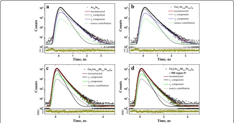
The measured raw PAL spectra are reconstructed from x2-term fitting procedure, these spectra for parent g-As2Se3, Ga-codoped g-Ga2(As0.40Se0.60)98, Ga-codoped and Sb-modified g-Ga2(As0.28Sb0.12Se0.60)98, Pr3+-doped (500 wppm) g-Ga2(As0.28Sb0.12Se0.60)98 being depicted on Fig. 1. The limited values of scatter of variance tightly grouped along 0-axis testify that PAL probing is adequately described within this fitting procedure. Therefore, decaying behavior of the PAL spectra on Fig. 1 can be reflected by sum of two negative exponentials with different time constants inversed to positron lifetimes. The best-fit positron trapping modes for the examined ChG calculated within two-state PT model [7–10, 21, 22] are given in Table 1.
Free-Volume Nanostructurization in Parent g-As2Se3 The parent g-As2Se3 possesses defect-specific lifetime τ2= 0.360 ns (Table 1) proper to this ChG as it follows
from numerous previous research [25–28]. The positron trapping in g-As2Se3is defined by PT-rateκd= 0.92 ns−
1
occurring under fraction of trapped positrons ηd= 0.19.
In respect to Jensen et al.’s DFT-calculations for orthorhombic As2Se3 crystal [27], this lifetime gives an
Fig. 1Raw PAL spectra of g-As40Se60(a), g-Ga2(As0.40Se0.60)98(b), g-Ga2(As0.28Sb0.12Se0.60)98(c), and Pr3+-doped (500 wppm) g-Ga2(As0.28Sb0.12Se0.60)98
[image:3.595.56.539.449.704.2]estimate for volume of PT defects near ~90 Å3. This open volume corresponds to 0.10 ns in (τ2-τb) difference
and 1.39 inτ2/τbratio, which can be accepted as a
signa-ture of extended triple-quadruple vacancies [7, 27]. It is difficult to define exactly which part of this free volume is atomic-accessible in glassy network in view of compli-cated inner structural configuration composed of inter-connected atom-shared AsSe3/2pyramids in g-As2Se3. In ref. [17], possible configuration of such PT free-volume voids were depicted at the map of electron-density distribution for isostructural mineral orpiment As2S3.
Structural genesis of expected PT sites in parent g-As2Se3 is conditionally illustrated on Fig. 2a assuming close to ellipsoidal shape for free-volume voids. The most efficient preferential PT sites are defined by extended free-volume spaces near Se atoms neighboring with AsSe3/2polyhedrons [26, 27]. Because of strong directionality of covalent chem-ical bonding in ChG, Se atoms form lower electron-density spaces known asbond-free solid angles(BFSA) in terms of Kastner [29]. Theseatomic-inaccessible BFSAcontribute to neighboring geometrical free volumes, ensuring effective negative electrical charge due to proximity with electro-negative Se atoms linked with more electropositive As. So, the BFSA originated from Se atoms form outer shell for inner geometrical hole of free-volume void, which can be identified in view of its preferential electric state as counter-parts of cation-type vacancy in crystals [7].
Therefore, the most efficient PT sites in g-As2Se3 can be imaged as free-volume voids formed within network of interlinked corner-shared AsSe3/2 pyramids, com-posed of atomic-accessible geometrical hole (void core) arrested by surrounding atomic-inaccessible Se-based BFSA (void shell), as it is illustrated in Fig. 2.
Free-Volume Nanostructurization Under Ga-Codoping
Effect of Ga-codoping in parent g-As2Se3, i.e., transition from g-As2Se3to g-Ga2(As0.40Se0.60)98, is revealed through gradual dropping in I2intensity accompanied by increase
in defect-specific τ2lifetime to 0.382 ns (Table 1). At the
basis of Jensen et al.’s [27] formalism, the latter can be ascribed to free volumes reaching as high as ~110 Å3. This jump in defect-specificτ2lifetime is ascribed to increased
average atomic coordination Z= 2.412 of g-Ga2(As0.40 Se0.60)98 due to Ga addition. Under such condition, the appeared Se2/2-As-As-Se2/2 bridges counterbalance Ga additions in g-As-Se, causing increased number of overlapped BFSA around end-terminated Se atoms contributing to PT sites [17, 28]. Thus, the Ga-codoping in g-As2Se3 results in agglomeration of existing PT sites (increase in their volume, but decrease in their content), thus leading to gradual decrease in PT-rate in defects κd
and, correspondingly, the fraction of trapped positronsηd
[image:4.595.58.539.100.204.2](see Table 1).
Table 1Fitting parameters and PT-modes describing two-component reconstructed PAL spectra in g-Gax[(As/Sb)0.40Se0.60]100-x
ChG sample Fitting parameters Positron trapping modes
τ1 τ2 I2 τav. τb κd τ2-τb τ2/τb ηd
ns ns a.u. ns ns ns−1 Ns – –
g-As40Se60 0.210 0.360 0.462 0.279 0.260 0.92 0.10 1.39 0.19
g-Ga2(As0.40Se0.60)98 0.223 0.382 0.401 0.287 0.267 0.75 0.11 1.43 0.17
g-Ga2(As0.28Sb0.12Se0.60)98 0.210 0.363 0.422 0.274 0.255 0.85 0.11 1.42 0.18
Pr3+-doped (500 wppm) g-Ga2(As0.28Sb0.12Se0.60)98
0.218 0.374 0.376 0.276 0.258 0.72 0.12 1.45 0.16
Fig. 2Genesis of free-volume PT-site in g-As-Se under subsequent nanostructurization stages evolving parent g-As40Se60(a), Ga-codoped
g-Ga2(As0.40Se0.60)98(b), Ga-codoped and Sb-modified g-Ga2(As0.28Sb0.12Se0.60)98(c), and Pr3+-doped (500 wppm) g-Ga2(As0.28Sb0.12Se0.60)98(d). The
[image:4.595.57.540.552.684.2]It is worth to note that PAL response on Ga-induced nanostructurization is fully determined by chemical composition of parent ChG. Thus, for example, in case of smaller Z= 2.30 character for TAS-235 glass (i.e., g-As30Se50Te20) [18], Ga-codoping does not change defect-specific τ2 lifetime, despite more pronounced
decrease in I2intensity. This result is fully concomitant
with small deviations observed inτ2lifetimes for Se-rich
ChG compositions in As-Se system [26, 28].
In general, such modification (when only atomic-deficient free-volume structure is changed) is unable to accommodate RE ions obeying electrically active state (RE3+), avoiding non-radiative decay [5, 14, 17, 18]. The FVE-accommodated RE dopants have to adopt an excess of positive electrical charge to ensure electrical compensa-tion throughout a glassy matrix. Successful resolucompensa-tion is based on possibility of Ga-codopants to reveal a metallic behavior being inserted in chalcogenide environment. In interaction with chalcogens, the Ga atoms create some polyhedrons (such as GaSe4/2 tetrahedra shown in the upper part on Fig. 2b), which are, from one side, topologically consistent with main network-forming polyhedrons to attain unique glassy arrangement having a large number of voids, but, from other side, these codopants can stabilize charge misbalance owing to local chalcogen (Se) over-coordination around Ga [14, 16, 30]. Under transition to g-Ga2(As0.40Se0.60)98, the GaSe4/2 tetrahedrons with favorable Ga-Se chemical bonds
appear in a network of corner-shared AsSe3/2
pyra-mids forming overall glassy matrix. Excess of
anion-type atoms occupying Se2− states around GaSe4/2
tetrahedrons causes the cloud of preferentially nega-tive electrical charge for neighboring free-volume void (as it is shown by enlarged outer shell in the consti-tution of PT site on Fig. 2b). In such a way, the more negatively charged voids of increased overall free volume in Ga-modified g-Ga2(As0.40Se0.60)98 serve as eventual precursors for charge-compensating incorporation of electrically active Pr3+ions.
Free-Volume Nanostructurization Under Sb-Modification
One of the parasitic drawbacks of Ga-codoping nanos-tructurization concerns in increased crystallization ability of Ga-contained ChG under further RE doping, since both Ga and RE chalcogenides possess isostructural crystalline polymorphs [5, 13]. In case of As-based ChG, this obstacle can be suppressed under partial As-to-Sb replacement [19]. This was a reason to turn towards nanostructurization in g-As-Se under Sb-modification.
In respect to atomic-deficient structure evidenced
from PAL spectroscopy, this Sb-substituted
g-Ga2(As0.28Sb0.12Se0.60)98demonstrates partial recovery to parent pure g-As2Se3. Indeed, in this ChG, the defect-specific lifetime τ2 is depressed down to 0.363 ns and
second component intensity I2 gets elevated to 0.422,
thus resulting in steadily increasing PT-rate in defects withκd=0.85 ns−1(Table 1). This Sb-modification is not
accompanied by change in PT-site type, since neither (τ2-τb) difference, nor τ2/τb ratio remains rather
unchanged within measuring error-bar.
Such effects are supposed to be defined by increase in an atomic packing of glassy network due to heavier (and more metallic) Sb atoms appeared instead of As ones (causing respective increase in ChG density from 4.64 to 4.90 g/cm3[19]). On Fig. 2c, these Sb-based structural en-tities are presented as SbSe3/2pyramidal units appeared in the nearest atomic surrounding of free-volume void. So PT sites in Sb-modified g-Ga2(As0.28Sb0.12Se0.60)98are like those in g-Ga2(As0.40Se0.60)98, but with slightly reduced outer free-volume shell mainly due to shielding effect from more metallic Sb-environment (Fig. 2c).
Free-Volume Nanostructurization Under RE Doping
Thus, in respect to these subsequent nanostructurization stages, the effect of RE doping can be treated in terms of competitive contribution of changed occupancy sites in the modified structure of g-Ga2(As0.28Sb0.12Se0.60)98 available for both RE ions and positrons. Indeed, from the point of affinity to negative electrical charge attached to neighboring free-volume space, the same type of
voids, which accommodate RE3+ ions, as shown in
Fig. 2d, can be attractive sites for annihilating positrons [6–10]. Under RE doping, the positively charged Pr3+ ions are stabilized in a glassy network due to strong Pr3+-Se-Ga covalent bridges (marked by dotted lines in Fig. 2d) [14, 31, 32], thus eliminating corresponding negatively charged void as potential positron traps. This void-collapse process results in PT-reduction, mainly due to essential decrease in second component intensity I2and rather slight increase in defect-specific lifetime τ2
(see Table 1), meaning that void volume is not essentially altered under RE doping.
Concentration of these PT free-volume defects in RE-doped ChG can be estimated accepting their analogy with negative cation-type vacancies in semiconductors giving trapping coefficients of approximately 1015atom⋅s−1 [7]. With known atomic densities and experimental PT-rate value for different ChG (Table 1), this estimation gives the defect concentration close to ~5⋅1016
under-margin content of embedded RE ions, which is typically beyond reliably detectable limits of these methods.
Conclusions
Atomic-deficient evolution of glassy arsenic selenides is traced in subsequent nanostructurization stages ensuring their RE-doping functionality, the positron annihilation lifetime spectroscopy being employed to parameterize free-volume positron trapping sites within known two-state trapping model. The most efficient positron traps in parent As2Se3glass are imagined as voids with character free volumes of ~90 Å3 formed in network of corner-shared AsSe3/2 pyramids, composed of atomic-accessible geometrical holes (void cores) arrested by surrounding atomic-inaccessible Se-based bond-free solid angles (void shell). Under Ga-codoping in Ga2(As0.40Se0.60)98 glass, these voids grow in size, being essentially modified by their environment to become preferen-tially negative, thus serving as precursors for charge-compensating incorporation of electrically active rare-earth ions. Vitreous state stabilizing modification with Sb addi-tives reduces outer free-volume shell of positron trapping sites mainly due to shielding effect from more metallic environment. The finalizing nanostructurization under Pr3+-doping (500 wppm) in Ga2(As0.28Sb0.12Se0.60)98glass is explained in terms of competitive contribution of changed occupancy sites available for both rare-earth ions and positrons.
Abbreviations
BFSA:Bond-free solid angles; ChG: Chalcogenide glasses; FVE: Free-volume elements; PAL: Positron annihilation lifetime; PT: Positron trapping; RE: Rare-earth
Acknowledgements
With a great pleasure I thank B. Bureau, C. Boussard-Pledel, and V. Nazabal (Glass and Ceramics Laboratory of University of Rennes 1) for their helpful assistance during glass preparation and input characterization. The valuable consulting on PALS experiments provided by Dr. Adam Ingram (Opole University of Technology) is also highly acknowledged.
Competing Interests
The author declares that he has no competing interests.
Author details
1Department of Sensor and Semiconductor Electronics, Ivan Franko National
University of Lviv, 107, Tarnavskogo str., Lviv 79017, Ukraine.2Center for Innovation and Transfer of Natural Sciences and Engineering Knowledge, Faculty of Mathematics and Natural Sciences, University of Rzeszow, 1, Pigonia str., 35-959 Rzeszow, Poland.3Laboratoire Verres et Céramiques, UMR-CNRS 6226, Université de Rennes 1, 35042 Rennes Cedex, France.
Received: 13 December 2016 Accepted: 27 February 2017
References
1. Feltz A (1986) Amorphous and vitreous inorganic solids. Mir, Moscow 2. Adam JL, Zhang X (eds) (2014) Chalcogenide glasses: preparation, properties
and applications. Woodhead publishing, Oxford-Cambridge-New Dehli 3. Cui S, Chahal R, Shpotyuk Y, Boussard C et al (2014) Selenide and telluride
glasses for mid-infrared biosensing. Proc SPIE 8938:893805
4. Lucas P, Bureau B (2017) Selenide glass fibers for biochemical infrared sensing. In: Ahluwalia GK (ed) Applications of Chalcogenides: S, Se, and Te. Springer, Cham, pp 285–322
5. Seddon AB, Tang Z, Furniss D, Sujecki S, Benson TM (2010) Progress in rare-earth-doped mid-infrared fiber lasers. Opt Express 18:26704–26719 6. Troles J, Coulombier Q, Canat G et al (2010) Low loss microstructured
chalcogenide fibers for large nonlinear effects at 1995 nm. Opt Express 18:26647–26654
7. Krause-Rehberg R, Leipner H (1999) Positron annihilation in semiconductors: defect studies. Springer, Heidelberg
8. Jean YC, Mallon PE, Schrader DM (2003) Principles and application of positron and positronium chemistry. World Sci. Publ. Co. Pte. Ltd., New
Jersy-London-Singapore-Hong Kong
9. Tuomisto F, Makkonen I (2013) Defect identification in semiconductors with positron annihilation: experiment and theory. Rev Mod Phys 85:1583–1631 10. Shpotyuk O, Filipecki J (2003) Free volume in vitreous chalcogenide
semiconductors: possibilities of positron annihilation lifetime study. WSP, Czestochowa
11. Shpotyuk Y, Bureau B, Boussard-Pledel C, Nazabal V, Golovchak R, Demchenko P, Polovynko I (2014) Effect of Ga incorporation in the As30Se50Te20glass. J Non-Cryst Solids 398–399:19–25
12. Shpotyuk O, Ingram A, Bureau B, Shpotyuk Y, Boussard-Pledel C, Nazabal V, Szatanik R (2014) Positron annihilation probing of crystallization effects in TAS-235 glass affected by Ga additions. J Phys Chem Solids 75:1049–1053
13. Shpotyuk Y, Boussard-Pledel C, Nazabal V, Chahal R, Ari J, Pavlyk B, Cebulski J, Doualan JL, Bureau B (2015) Ga-modified As2Se3–Te glasses
for active applications in IR photonics. Opt Mater 46:228–232 14. Aitken BG, Ponader CW, Quimby RS (2002) Clustering of rare earths in GeAs
sulfide glass. CR Chimie 5:865–872
15. Churbanov MF, Scribachev IV, Shiryaev VS, Plotnichenko VG, Smetanin SV, Kryukova EB, Pyrkov YN, Galagan BI (2013) Chalcogenide glasses doped with Tb, Dy and Pr ions. J Non-Cryst Solids 326–327:301–305
16. Golovchak R, Shpotyuk Y, Nazabal V, Boussard-Pledel C, Bureau B, Cebulski J, Jain H (2015) Study of Ga incorporation in glassy arsenic selenides by high-resolution XPS and EXAFS. J Chem Phys 142:184501
17. Shpotyuk Y, Ingram A, Shpotyuk O, Dziedzic A, Boussard-Pledel C, Bureau B (2016) Free-volume nanostructurization in Ga-modified As2Se3glass.
Nanoscale Res Lett 11:20
18. Shpotyuk Y, Ingram A, Shpotyuk O, Boussard-Pledel C, Nazabal V, Bureau B (2016) Effect of rare-earth doping on the free-volume structure of Ga-modified Te20As30Se50glass. RSC Adv 6:22797–22802
19. Shpotyuk Y, Boussard-Pledel C, Nazabal V, Bureau B (2017) The influence of Sb on glass forming ability of Ga-containing As2Se3glasses. J Am Ceram
Soc. doi:10.1111/jace.14662
20. Kansy J (1996) Microcomputer program for analysis of positron annihilation lifetime spectra. Nucl Instrum Methods Phys Res, Sect A 374:235–244 21. Seeger A (1974) The study of defects in crystals by positron annihilation.
Appl Phys 4:183–199
22. Keeble DJ, Brossmann U, Puff W, Würschum R (2012) Positron annihilation studies of materials. In: Kaufmann EN (ed) Characterization of materials. John Wiley & Sons, Inc., pp 1899–1925
23. Shpotyuk M, Ingram A, Shpotyuk O (2015) Characterization of radiation-induced effects in amorphous arsenic sulfides by positron annihilation. J Mater Res 30:1422–1429
24. Ghosh S, Nambissan PMG, Bhattacharya R (2004) Positron annihilation and Mössbauer spectroscopic studies of In3+substitution effects in bulk and
nanocrystalline MgMn0.1Fe1.9−xInxO4. Phys Lett A 325:301–308
25. Alekseeva OK, Mihailov VI, Chernov AP, Shantarovich VP (1977) Point structural defects studied in chalcogenide semiconductors by positron annihilation. Sov Fiz Tverd Tela 19:3452–3454
26. Alekseeva OK, Mihajlov VI, Shantarovich VP (1978) Positron annihilation in point defects of the glassy As-Se system. Phys Stat Solidi A 48:K169–K173 27. Jensen KO, Salmon PS, Penfold IT, Coleman PG (1994) Microvoids in
chalcogenide glasses studied by positron annihilation. J Non-Cryst Solids 170:57–64
28. Ingram A, Golovchak R, Kostrzewa M, Wacke S, Shpotyuk M, Shpotyuk O (2012) Compositional dependences of average positron lifetime in binary As-S/Se glasses. Phys B 407:652–655
30. Golovchak R, Shpotyuk Y, Thomas CM, Nazabal V, Boussard-Pledel C, Bureau B, Jain H (2015) Peculiarities of Ga and Te incorporation in glassy arsenic selenides. J Non-Cryst Solids 429:104–111
31. Lee TH, Simdyankin SI, Su L, Elliott SR (2009) Evidence of formation of tightly bound rare-earth clusters in chalcogenide glasses and their evolution with glass composition. Phys Rev B 79:180202
32. Lee TH, Simdyankin SI, Hegedus J, Heo J, Elliott SR (2010) Spatial distribution of rare-earth ions and GaS4tetrahedra in chalcogenide
glasses studied via laser spectroscopy and ab initio molecular dynamics simulation. Phys Rev B 81:104204
Submit your manuscript to a
journal and benefi t from:
7 Convenient online submission
7Rigorous peer review
7 Immediate publication on acceptance
7Open access: articles freely available online
7 High visibility within the fi eld
7Retaining the copyright to your article
![Table 1 Fitting parameters and PT-modes describing two-component reconstructed PAL spectra in g-Gax[(As/Sb)0.40Se0.60]100-x](https://thumb-us.123doks.com/thumbv2/123dok_us/8849745.934429/4.595.57.540.552.684/table-fitting-parameters-modes-describing-component-reconstructed-spectra.webp)
