N A N O E X P R E S S
Open Access
Optical Constants and Band Gap Evolution
with Phase Transition in Sub-20-nm-Thick
TiO
2
Films Prepared by ALD
Yue-Jie Shi
1, Rong-Jun Zhang
1*, Hua Zheng
1, Da-Hai Li
1, Wei Wei
2, Xin Chen
2*, Yan Sun
2, Yan-Feng Wei
2,
Hong-Liang Lu
3, Ning Dai
2and Liang-Yao Chen
1Abstract
Titanium dioxide (TiO2) ultrathin films with different thicknesses below 20 nm were grown by atomic layer deposition (ALD) on silicon substrates at 300 °C. Spectroscopic ellipsometry (SE) measurements were operated to investigate the effect of thickness on the optical properties of ultrathin films in the spectra range from 200 to 1000 nm with Forouhi–Bloomer (F-B) dispersion relation. It has been found that the refractive index and extinction coefficient of the investigated TiO2ultrathin film increase while the band gap of TiO2ultrathin film decreases monotonically with an increase in film thickness. Furthermore, with the purpose of studying the temperature dependence of optical properties of TiO2ultrathin film, the samples were annealed at temperature from 400 to 900 °C in N2atmosphere. The crystalline structure of deposited and annealed films was deduced by SE and
supported by X-ray diffraction (XRD). It was revealed that the anatase TiO2film started to transform into rutile phase when the annealing temperature was up to 800 °C. In this paper, a constructive and effective method of
monitoring the phase transition in ultrathin films by SE has been proposed when the phase transition is not so obvious analyzed by XRD.
Keywords:TiO2ultrathin film, Atomic layer deposition, Spectroscopic ellipsometry, Rapid thermal annealing, Phase transition
Background
Titanium dioxide (TiO2) became a promising material in
different applications for its excellent optical and electrical properties and chemical stability such as large band gap, high refractive index, high dielectric constant, and highly active surface [1–4]. Traditionally, TiO2 pigment has
almost been applied to every kind of paint due to its high refractive index [5, 6] and used as photocatalyst in the process of sterilizing, deodorizing, antifouling, and so on, which can convert light energy into electrical energy and chemical energy [6–8]. Moreover, the high dielectric constant (k~ 80) of TiO2 allows it to take the place of
traditional silicon dioxide (SiO2), used as capacitors in
dynamic random access memory (DRAM) devices or ultrathin gate dielectric layers in field-effect transistors (FET) [9, 10]. Now, ultrathin TiO2layers as a barrier with
a mean thickness of <3 nm could enhance photovoltaic performance of the inverted organic solar cell, especially short-circuit current (Jsc) and power conversion efficiency
(PCE) [11]. Furthermore, metalenses at visible wave-lengths with efficiencies as high as 86% have been demon-strated recently by using TiO2 materials, in which TiO2
could overcome the challenge of the high intrinsic losses in the visible range and realize the highly efficient meta-surfaces in this region [12]. TiO2has been one of the most
studied materials in the last decades, and numerous re-search concerning TiO2bulks and films have been already
reported [1–4]. However, the research on the optical prop-erties of TiO2 ultrathin films, especially below 20 nm, is
still rare. Thus, detailed studies on the optical properties of sub-20-nm TiO2films have become very important to
the miniaturization of integrated photonic devices, the
* Correspondence:[email protected];[email protected] 1Key Laboratory of Micro and Nano Photonic Structures, Ministry of
Education, Department of Optical Science and Engineering, Fudan University, Shanghai 200433, China
2National Laboratory for Infrared Physics, Shanghai Institute of Technical
Physics, Chinese Academy of Sciences, Shanghai 200083, China Full list of author information is available at the end of the article
performance of solar cell devices, and even the application of metalenses [11–13].
TiO2thin films can be prepared by various methods such
as electron beam evaporation, laser-assisted evaporation,
chemical vapor deposition, sol–gel process, sputtering, and atomic layer deposition (ALD) [14]. Among them, the ALD method has been usually adopted to grow ultrathin and high-k dielectrics owing to its advantages over other
50 cycles 100 cycles
200 cycles 300 cycles
400 cycles 500 cycles
600 cycles
a
b
c
d
e
f
g
h
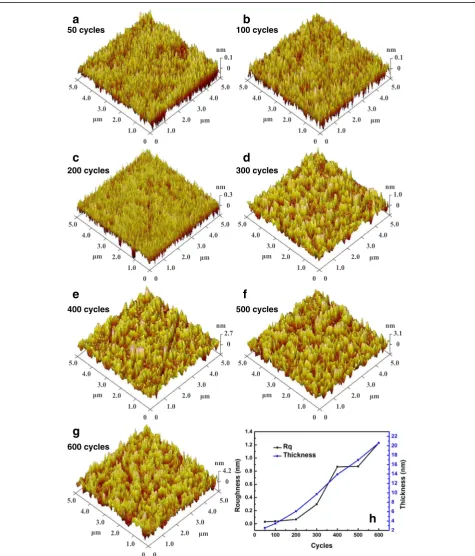
Fig. 1AFM micrographs of as-deposited TiO2ultrathin films with different thicknesses.a50 cycles.b100 cycles.c200 cycles.d300 cycles.
[image:2.595.60.536.145.702.2]methods in completely precise thickness control, low pro-cessing temperature, low impurity content, no line-of-sight depositions, conformal coating capability on complex-shaped structures, and excellent thickness uniformity over large deposition area [1, 3, 15–17].
This work is focused on the study of optical properties of TiO2 ultrathin film, whose thickness is less than
20 nm. To achieve high-quality TiO2ultrathin films, the
ALD method has been employed to deposit samples on single crystal Si substrates. Furthermore, we investigate those films mainly by spectroscopic ellipsometry (SE), a powerful non-destructive and sensitive technique. The optical constants and optical band gap of the TiO2ultrathin
film are obtained, and the influence of nano size and temperature on the optical properties is also revealed. These results will be helpful to the applications of ultrathin TiO2 in optoelectronic semiconductor devices such as
memory, field-effect transistors, and inverted organic solar cells. What is more, a novel method to monitor the phase transition in ultrathin films is proposed by deducing from the band gap evolution.
Methods
TiO2ultrathin films were fabricated on Si (100) substrates
by ALD (Picosun R-series, Espoo, Finland). The substrates were heated using a resistive heating plate, providing tem-peratures up to 300 °C. Titanium tetraisopropoxide (TTIP) was the precursor for titanium, and H2O was the
precursor for oxygen. The bubbler containing TTIP was heated to 80 °C. High purity N2gas was used to purge the
reactor chamber after each precursor pulse. Each ALD cycle consists of four steps: first, 0.5 s to pulse TTIP; then, 10 s to purge the chamber; next, 0.1 s to pulse H2O as the
second reactant; eventually, 10 s to evacuate H2O [18].
After deposition, the as-deposited films were annealed by a rapid thermal process (RTP; AS-ONE, Montpellier, France) system at the temperatures of 400–900 °C with an increment of 100 °C in N2atmosphere. Then,
spec-troscopic ellipsometry (SE; J. A. Woollam Co. M2000X-FB-300XTF, Lincoln, NE, USA) measurements were
performed in order to examine the influence of micro-structure characteristics on the optical properties of the films. All the films were characterized before and after annealing in the wavelength range from 200 to 1000 nm at the incident angle of 65 °C. The surface morphologies of films were studied using atomic force microscopy (AFM; Bruker Dimension Icon VT-1000, Santa Barbara, CA, USA) in tapping mode. The crystalline structures of films were also examined by X-ray diffraction (XRD; Bruker-AXS D8) and transmission electron microscope (TEM; FEI Tecnai G2 F20, Hillsboro, OR, USA). Besides, the reflection spectra (Lamda 950; PerkinElmer Instru-ments Co.) were measured to verify the band gap evolution and support the SE results.
Results and Discussion
The TiO2ultrathin films with different thicknesses were
obtained by controlling the numbers of ALD cycles from 50 to 600 cycles. In order to identify the quality of as-de-posited films and make SE measurements more effectively in characterizing the samples, information concerning the structure and morphology is an essential prerequisite. This information is conductive to establish the optical model and adopt a suitable dispersion law for calculating dielectric function in SE process [19, 20]. In consequence, the AFM, XRD, and TEM results of the as-deposited films were ana-lyzed firstly.
The 3D AFM micrographs (scanning area 5 μm × 5μm) are shown in Fig. 1. The surface morphologies of all films are smooth with different root mean square (RMS) roughness values (vary from 0.03 to 1.23 nm), which indicates that TiO2 ultrathin films were well
fabricated (Fig. 1h). The small surface roughness can reduce the light scattering caused by rough surface in SE measurements [3].
[image:3.595.59.539.88.220.2]Fig. 2aXRD patterns for all films of different cycles grown on Si (100) substrates.bTEM micrograph for TiO2ultrathin film of 600 cycles
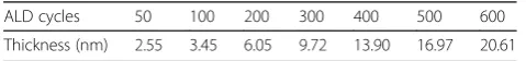
Table 1Thicknesses of TiO2ultrathin films calculated by SE
ALD cycles 50 100 200 300 400 500 600
[image:3.595.303.543.703.731.2]The XRD patterns of all films with different thick-nesses are given in Fig. 2a. The films, deposited below 300 ALD cycles, do not show any XRD peaks of TiO2,
indicating those films have low crystallinity or even are amorphous in nature because TiO2 nanostructures in
early ALD process evolve from amorphous layers to
amorphous particles to metastable crystallites and finally to stable crystalline forms, which is a manifestation of the Ostwald–Lussac law [16]. When the ALD cycles are above 400, TiO2ultrathin films begin to exhibit an anatase (101)
peak at 2θ= 25.4° [21]. The intensity of anatase (101) peak is found to increase with increasing cycles, showing that
Fig. 3aRefractive indexnandbextinction coefficientkspectra for TiO2ultrathin films with different thicknesses. Theinsetofashows the plot
of peak position versus ALD cycles
[image:4.595.59.542.88.219.2] [image:4.595.59.534.356.715.2]the crystalline becomes better as film thickness increases. The mean grain size of the prepared TiO2nano crystalline
is 13.9 nm for the sample of 400 cycles, 17.1 nm for the sample of 500 cycles, and 20.5 nm for the sample of 600 cycles, calculated from the (101) diffraction peaks using Scherrer’s formula [22]. The gains with smaller size in thinner films could contribute to the close-packed nanocrystallites and larger crystalline volume fraction, resulting in lowerRq. Hence, the increasing grain size can
also explain the increasing surface RMS roughness varying with the increasing thickness in Fig. 1h [3]. Furthermore, on account of the phase transformation from amorphous state to crystalline state as implied in Fig. 2a, an increased RMS roughness of ~1 nm is observed in Fig. 1 when the cycles are above 400. The TEM result of 600 cycles TiO2
is provided in Fig. 2b. There is no denying the fact that an interface layer exists between Si and TiO2obviously and
the thickness of interface layer is about 1 nm.
Then, the optical properties of TiO2 ultrathin films
were investigated by spectroscopic ellipsometry (SE). SE is well-known for its non-contact and non-destructive measurement and applies in extracting the thickness, optical constants, and band gap by a proper optical model [23]. The ellipsometric parameters Ψ and Δ are defined by the ellipsometric ratioρas [23, 24]:
ρ¼rs=rp ¼ tanΨexpð ÞjΔ ð1Þ
whererpand rsare the complex reflection coefficients of
polarized light parallel and perpendicular to the inci-dence plane, respectively. As the surface roughnesses of TiO2films are very small according to the AFM
micro-graphs and the cross-sectional structure shown in TEM
micrographs, an optical model comprising air/TiO2/Ti
x-SiyO2/Si is established in the fitting process to reduce
the uncertainty of fitting [25].
The Forouhi–Bloomer (F-B) dispersion model is consid-ered to describe the optical constants of TiO2[23]. The F-B
dispersion model is of benefit to determining the refractive indexnand extinction coefficientkvalues accurately, which could provide a decent description of the excitations near the absorption threshold in disordered dielectrics. F-B dispersion model is described as follows [23, 26]:
n Eð Þ ¼nð Þ þ∞ X
i
B0iEþC0i
E2−B
iEþCi ð2Þ
k Eð Þ ¼X i
AiðE−EgÞ
E2−B
iEþCi ð3Þ
where n(∞) is the refractive index when photon
en-ergy E→∞, Eg is the band gap of TiO2, B0i¼QAii
−Bi2
2 þEgBi−Eg2þCi
h i
, C0i¼AiQi Eg
2þC
i
Bi
2−2EgC
,
Qi¼12 4Ci−Bi2
1=2
, and Ai, Bi, Ci are positive
non-zero parameters characteristic of the medium such that 4Ci−Bi2> 0. In addition, to characterize the
fit-ting precision, the root mean square error (RMSE) is described as [23, 24]:
RMSE ¼
ffiffiffiffiffiffiffiffiffiffiffiffiffiffiffiffiffiffiffiffiffiffiffiffiffiffiffiffiffiffiffiffiffiffiffiffiffiffiffiffiffiffiffiffiffiffiffiffiffiffiffiffiffiffiffiffiffiffiffiffiffiffiffiffiffiffiffiffiffiffiffiffiffiffiffiffiffiffiffiffiffiffiffiffiffiffiffiffi 1
2N−M−1 XN
i¼1
Ψcal i −Ψexpi
2
þ Δcal i −Δexpi
2 h i v u u t
ð4Þ
[image:5.595.54.292.98.127.2]whereNis the number of data points in the spectra,M is the number of variable parameters in the model, and “exp” and “cal” represent the experimental and the cal-culated data, respectively [27]. The fitting results are considered ideal until the RMSE value is less than 1 [23]. Table 2Band gaps of TiO2ultrathin films
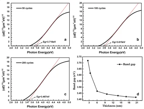
Cycles 50 100 200 300 400 500 600
Band gap (eV) 3.718 3.615 3.467 3.443 3.430 3.422 3.417
Fig. 5aRefractive indexnspectra andbextinction coefficientkspectra for TiO2ultrathin films with different thicknesses after annealing at 400 °C.
The insert ofashows plot of peak position versus ALD cycles. The insert ofbshows plots of (αE)1/2vs.Efor TiO
2ultrathin films with different
[image:5.595.59.540.562.693.2]The thicknesses of films calculated by SE are listed in Table 1. As we can see, all the samples except for those of 50 cycles grew at a stable speed of ~0.34 Å/cycle. In order to study the cause of different growth rates of those of 50 cycles, we also have studied the growth rate of films with ALD cycles below 50. It is found that the growth rate is still changeable and varies from 0.36 to 0.44 Å/cycle. Therefore, we hold the opinion that two reasons could cause that. On the one hand, the early ALD growth process is not stable and is in the process of nucleation. On the other, SE results exist at a certain degree of calculation error for ~0.3 nm, which could lead to a considerable calculation error to growth rate (~0.1 Å/cycle when ALD cycles are below 50).
Figure 3 displays the dispersion curves of refractive indices (n) and extinction coefficients (k). It is noticed in Fig. 3a that refractive indices increase with the increasing thicknesses of films, which is most caused by the density of films [28]. The volume ratio of air in the layer decreases when the thickness of film increases [13]. Moreover, the peak of refractive index occurs redshift with the increase of thickness, which is due to the redshift of the anomalous dispersion region (inset of Fig. 3a). Figure 3b explains that extinction coefficients increase gradually with the increas-ing thickness, consistent with the tendency of refractive indices. The absorption edge also shows an obvious redshift, indicating a decrease of band gap.
Fig. 6Reflection spectra of TiO2ultrathin filmsabefore andbafter annealing at 900 °C
Fig. 7Plots of (αE)1/2vs.Efor TiO
2ultrathin films ofa600 cycles caculated by the F-B dispersion model,b600 cycles caculated by the
[image:6.595.57.540.425.691.2]In order to quantify the variation of band gap, linear extrapolation of absorption coefficient αwas conducted to determine the band gap energy evolution of TiO2
films with the formula described as [23]:
α¼4πλk¼K E−Eg
m
E ð5Þ
where k is the extinction coefficient, λ is the incident wavelength,Kis the constant,Eis the photon energy,Eg
is the band gap, and m is the number decided by the transition process, specifically divided into two kinds of situations:mequals to 1/2 for direct transition and 2 for indirect transition [23, 29]. The amorphous and anatase TiO2 have an indirect band gap, so them should be 2.
Figure 4 shows the plots of (αE)1/2 vs. E for three sam-ples, and Table 2 lists all the band gaps of seven samples. It is obviously found that the value of band gap declines from 3.718 to 3.417 eV with the increasing thickness (Fig. 4d), as a result of quantum confinement effect [13, 30]. The decrease of the size of material leads to the increase of the band gap. Meanwhile, the smaller band gap in thicker film could cause a redshift of the anomalous dispersion region as illustrated in Fig. 3.
To investigate the temperature dependence of optical properties of TiO2 ultrathin films, the samples were
annealed at the temperatures of 400, 500, 600, 700, 800, and 900 °C, respectively. Figure 5a, b shows the optical constants of TiO2 ultrathin films with different
thick-nesses after annealing at the same temperature of 400 °C. It can be found that the rapid thermal process (RTP) does not destroy the regularity of optical constants varying with thickness. The refractive index and the extinction coeffi-cient become higher with the increase of the thickness, while the band gap of TiO2ultrathin films appears to have
an opposite trend, as inferred from the inset of Fig. 5b. Figure 6 displays the reflection spectra of TiO2
ultra-thin films before and after annealing at 900 °C. It can be seen clearly that the absorption edge sinks after anneal-ing, especially for samples of 300, 400, and 500 cycles, indicating that the annealing process is very effective [31]. Furthermore, absorption edge has a redshift with increasing thickness before and after annealing, which illustrates the decrease of band gap. This also verifies the regularity of band gap evolution changing with thickness obtained via SE before.
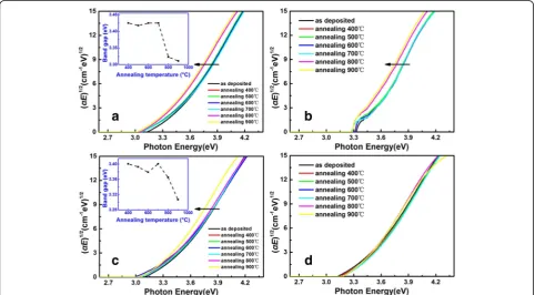
With the purpose of studying the variation of optical properties under different annealing temperatures, sam-ples of 600 cycles were selected and annealed in the range of 400 to 900 °C with an increment of 100 °C. As can be seen in Fig. 7a, absorption edge suddenly pre-sents a shift and the band gap of TiO2 ultrathin films
decreases suddenly (inset of Fig. 7a) when the films were annealed at 800 and 900 °C. Then, the point-by-point
data inversion method is employed to verify the accuracy of the reduction of band gap, as shown in Fig. 7b. It is found that the annealing temperature of 800 and 900 °C do cause a decrease of band gap.
Meanwhile, samples of 500 and 300 cycles after an-nealing were also selected to conduct SE analysis, as shown in Fig. 7c, d. The TiO2 film of 500 cycles also
appears to have a sharp decrease of band gap at 900 °C (inset of Fig. 7c), while the film of 300 cycles does not. It is conjectured that crystalline phase has been changed from anatase to rutile phase by high temperature anneal-ing for the samples of 600 and 500 cycles, while the samples of 300 cycles are still amorphous [4, 32]. Ac-cording to the previously reported research, the band gap of anatase bulk TiO2 is 3.23 eV, while that of the
rutile bulk TiO2 is 3.02 eV [5], which is in accordance
with the decrease of band gap described above, whereas there is no such phenomenon in the TiO2 ultrathin film
[image:7.595.305.539.361.684.2]with ALD cycles fewer than 300, owing to no crystallization in extremely thin films.
Figure 8a presents the XRD patterns for films of 600 cycles after annealing, in which exists an obvious
anatase (101) peak at the annealing temperature of 400–700 °C. When the annealing temperature is as high as 800 °C, the anatase peak disappears suddenly and a rutile (110) peak emerges gradually at 2θ= 27.5° [4]. It has been proved that the shift of band gap in Fig. 7a, b is caused by phase transformation.
The XRD patterns for films of 500 and 300 cycles after annealing are also given in Fig. 8. For the former films, the anatase (101) peak disappears when the annealing temperature is up to 800 °C and the rutile (110) peak appears instead at 900 °C (Fig. 8b). And the latter films, as can be seen in Fig. 8c, are always amorphous before and after annealing. Thus, these results are consistent with the calculated results of SE.
Conclusions
In summary, TiO2ultrathin films with high purity were
grown in a self-limited ALD growth mode by using TTIP as Ti precursors on silicon substrates at a substrate temperature of 300 °C. The TiO2layers were characterized
with respect to microstructure, composition, optical con-stants, and optical band gap by atomic force microscopy, X-ray diffraction, reflectance spectroscopy, and spectro-scopic ellipsometry.
The effect of thickness on the optical properties of TiO2ultrathin films has been investigated. The refractive
index and absorption coefficient increase with the in-creasing film thickness, attributed to the effect of pore. On the other hand, the quantum size effect could cause the variation of band gap. Then, the as-deposited films were annealed at the temperature of 400 to 900 °C in N2
atmosphere. It is found that thermal annealing does not destroy the regularity of optical constants. As for the TiO2 ultrathin films with ALD cycles above 400, high
temperature around 800 °C transforms the anatase TiO2
to rutile TiO2 via deducing from band gap evolution,
which provides a novel method to detect the phase tran-sition in ultrathin films. The results in this paper about TiO2ultrathin films will play a role in the future
applica-tion of optoelectronic devices.
Abbreviations
AFM:Atomic force microscopy; ALD: Atomic layer deposition; DRAM: Dynamic random access memory; F-B: Forouhi–Bloomer; FET: Field-effect transistors; PCE: Power conversion efficiency; RMS: Root mean square; RMSE: Root mean square error; RTP: Rapid thermal process; SE: Spectroscopic ellipsometry; SiO2: Silicon dioxide; TEM: Transmission electron microscope; TiO2: Titanium
dioxide; TTIP: Titanium tetraisopropoxide; XRD: X-ray diffraction
Acknowledgements
The work was financially supported by the National Natural Science Foundation of China (Nos. 11174058, 11674062, and 61376016), the no. 2 National Science and Technology Major Project of China (No. 2011ZX02109-004), MOST (No. 2016YFA0202201), Youth Innovation Promotion Association CAS and State Key Laboratory of ASIC and System, Fudan University (No. 2015KF003).
Authors’Contributions
YJS performed the experiment of the TiO2ultrathin films and drafted the
manuscript. RJZ and XC proposed the initial work and finalized the manuscript. HZ, DHL, and WW provided guidance and assistance in the experiment. YS, YFW, and HLL participated in the design and coordination of the study. ND and LYC supervised the work. All authors read and approved the final manuscript.
Competing Interests
The authors declare that they have no competing interests.
Publisher’s Note
Springer Nature remains neutral with regard to jurisdictional claims in published maps and institutional affiliations.
Author details
1Key Laboratory of Micro and Nano Photonic Structures, Ministry of
Education, Department of Optical Science and Engineering, Fudan University, Shanghai 200433, China.2National Laboratory for Infrared Physics, Shanghai
Institute of Technical Physics, Chinese Academy of Sciences, Shanghai 200083, China.3State Key Laboratory of ASIC & System, Fudan University,
Shanghai 200433, China.
Received: 25 November 2016 Accepted: 19 March 2017
References
1. Aydin SBK, Yildiz DE, ÇavuşHK et al (2014) ALD TiO2thin film as dielectric
for Al/p-Si Schottky diode. B Mater Sci 37(7):1563–1568
2. Zhang Y, Creatore M, Ma QB et al (2015) Nitrogen-doping of bulk and nanotubular TiO2photocatalysts by plasma-assisted atomic layer deposition.
Appl Surf Sci 330:476–486
3. Saha D, Ajimsha RS, Rajiv K et al (2014) Spectroscopic ellipsometry
characterization of amorphous and crystalline TiO2thin films grown by atomic
layer deposition at different temperatures. Appl Surf Sci 315(10):116–123 4. Jin C, Liu B, Lei Z et al (2014) Structure and photoluminescence of the TiO2
films grown by atomic layer deposition using tetrakis-dimethylamino titanium and ozone. Nanoscale Res Lett 10(1):1–9
5. King DM, Liang X, Carney CS et al (2008) Atomic layer deposition of UV-absorbing ZnO films on SiO2and TiO2nanoparticles using a fluidized bed
reactor. Adv Funct Mater 18(4):607–615
6. Iancu AT, Logar M, Park J et al (2015) Atomic layer deposition of undoped TiO2exhibiting p-type conductivity. ACS Appl Mater Inter 7(9):5134–5140
7. Zhang X, Zhang T, Ng J et al (2009) High-performance multifunctional TiO2
nanowire ultrafiltration membrane with a hierarchical layer structure for water treatment. Adv Funct Mater 19(23):3731–3736
8. Henry J, Balikdjian D, Storme G et al (2007) Photocatalytic and antibacterial activity of TiO2and Au/TiO2nanosystems. Nanotechnology 18(37):14026–14029
9. Kim SK, Choi GJ, Sang YL et al (2008) Al-doped TiO2films with ultralow
leakage currents for next generation DRAM capacitors. Adv Mater 20(8): 1429–1435
10. Xie Q, Deduytsche D, Schaekers M et al (2010) Implementing TiO2as gate
dielectric for Ge-channel complementary metal-oxide-semiconductor devices by using HfO2/GeO2interlayer. Appl Phys Lett 97(11):112905,
-112905-3
11. Seo HO, Park SY, Shim WH et al (2011) Ultrathin TiO2films on ZnO
electron-collecting layers of inverted organic solar cell. J Phys Chem C 115(43): 21517–21520
12. Khorasaninejad M, Chen WT, Devlin RC et al (2016) Metalenses at visible wavelengths: diffraction-limited focusing and subwavelength resolution imaging. Science 352(6290):1190–1194
13. Xu ZJ, Zhang F, Zhang RJ et al (2013) Thickness dependent optical properties of titanium oxide thin films. Appl Phys A-Mater 113(3):557–562 14. Chen X, Mao SS (2007) Titanium dioxide nanomaterials: synthesis,
properties, modifications, and applications. Chem Rev 107(7):2891–959 15. Niu W, Li X, Karuturi SK et al (2015) Applications of atomic layer deposition
in solar cells. Nanotechnology 26(6):064001–064001
16. Shi J, Li Z, Kvit A et al (2013) Electron microscopy observation of TiO2
17. Lu HL, Sun L, Ding SJ et al (2006) Characterization of atomic-layer-deposited Al2O3/GaAs interface improved by NH3plasma pretreatment. Appl Phys Lett
89(15):152910, -152910-3
18. Xie Q, Jiang YL, Detavernier C et al (2007) Atomic layer deposition of TiO2
from tetrakis-dimethyl-amido titanium or Ti isopropoxide precursors and H2O. J Appl Phys 102(8):083521 083521-6
19. Horprathum M, Kaewkhao J, Eiamchai P et al (2013) Investigation of inhomogeneity of TiO2thin films using spectroscopic ellipsometry. J Phys
Conf Ser 417(1):012007
20. Mosaddequrrahman M, Yu G, Soga T et al (2000) Refractive index and degree of inhomogeneity of nanocrystalline TiO2thin films: Effects of
substrate and annealing temperature. J Appl Phys 88(8):4634–4641 21. Ghrairi N, Bouaicha M (2012) Structural, morphological, and optical
properties of TiO2thin films synthesized by the electro phoretic deposition
technique. Nanoscale Res Lett 7(1):1–7
22. Gao K, Zhang W, Sun J et al (2009) Influences of substrate and annealing on the structural and optical properties and photoluminescence of
nanocrystalline ZnO films prepared by plasma assisted pulsed laser deposition. J Phys Chem C 113(44):19139–19144
23. Fujiwara H (2007) Spectroscopic ellipsometry: principles and applications. John Wiley & Sons, Chichester
24. Tompkins HG, Irene EA (2005) Handbook of ellipsometry. William Andrew, Norwich, pp 481–566
25. Wang ZY, Zhang RJ, Lu HL et al (2015) The impact of thickness and thermal annealing on refractive index for aluminum oxide thin films deposited by atomic layer deposition. Nanoscale Res Lett 10(1):1–6
26. Forouhi AR, Bloomer II (1986) Optical dispersion relations for amorphous semiconductors and amorphous dielectrics. Ann of Intern Med 34(10):7018–7026
27. Xu JP, Zhang RJ, Chen ZH et al (2014) Optical properties of epitaxial BiFeO3
thin film grown on SrRuO3-buffered SrTiO3substrate. Nanoscale Res Lett
9(1):1–6
28. Cai QY, Zheng YX, Mao PH et al (2010) Evolution of optical constants of silicon dioxide on silicon from ultrathin films to thick films. J Phys D Appl Phys 43(44):445302–445307
29. Yim C, O'Brien M, Mcevoy N et al (2014) Investigation of the optical properties of MoS2thin films using spectroscopic ellipsometry. Appl Phys
Lett 104(10):103114, -103114-5
30. Yu X, Zhang RJ, Xu ZJ et al (2011) Optical constants and band gap expansion of size controlled silicon nanocrystals embedded in SiO2matrix.
J Non-Cryst Solids 357(357):3524–3527
31. Straňák V,Čada, Martin, Quaas M et al (2009) Physical properties of homogeneous TiO2films prepared by high power impulse magnetron
sputtering as a function of crystallographic phase and nanostructure. J Phys D Appl Phys 42(42):105204–105215
32. Zheng H, Zhang RJ, Xu JP et al (2016) Thickness-dependent optical constants and annealed phase transitions of ultrathin ZnO films. J Phys Chem C 120:22532–22538
Submit your manuscript to a
journal and benefi t from:
7Convenient online submission
7Rigorous peer review
7Immediate publication on acceptance
7Open access: articles freely available online
7High visibility within the fi eld
7Retaining the copyright to your article