© 2017, IRJET | Impact Factor value: 5.181 | ISO 9001:2008 Certified Journal
| Page 270
CAPACITORLESS LDO FOR HIGH FREQUENCY APPLICATIONS
Jeyashri.M
1, SeemaSerin.A.S
2, Vennila.P
3, Lakshmi Priya.R
41
PG Scholar, Department of ECE, Theni Kammavar Sangam College of Technology, Tamilnadu, India.
2PG Scholar, Department of ECE, Theni Kammavar Sangam College of Technology, Tamilnadu, India.
3PG Scholar, Department of ECE, Theni Kammavar Sangam College of Technology, Tamilnadu, India.
4
Assistant Professor, Department of ECE, Theni Kammavar Sangam College of Technology, Tamilnadu, India.
---***---
Abstract –
Power saving is importa nt in all portable electronic devices like cellular phones and PDAs. This is essential to reduce the standby power and improve the battery runtime. Single stage regulator topologies are mainly used in embedded applications because of low power consumption. A single stage and adaptive biased low-dropout regulator is used to achieve a comparable dc load regulation. This is done mainly by modifying the adaptive bias loop which improves both the differential mode signals as well as common-mode signals. In addition, the proposed regulator is stable for a wide range of logics with variable capacitors and also for the capacitor-less conditions. The proposed regulator is implemented in a standard 0.18-μm CMOS technology.Key Words
:
Low Drop-Out (LDO) regulator, Adaptivebiasing, Single Stage Regulator, CMOS Technology, Load Regulation.
1. INTRODUCTION
A low-dropout (LDO) regulator is providing a clean supply due to low noise, ripple-free characteristics and less area. LDO regulator is used to supply a high load current demand, for a major challenge to maintain the dc accuracy of the output voltage. In electronics circuits, the dropout voltage of a regulator is the difference between the output voltage and input voltage. Dropout voltage for a general purpose integrated circuit regulator can high as 2 Volt, but low dropout regulators have a dropout of less than 100 mV at full load of the circuit. The load is very depending on the load for the dropout voltage in the regulator. Higher load will increasing usually, due to the regulator's pass transistor and circuitry of the internal resistance. Dropout voltage varies to temperature is varied. Dropout voltage is specified range of temperatures as well as load. Determine the efficiency of the voltage regulator in the Dropout voltage and quiescent current. Dropout voltage is low due to improve efficiency. A low-dropout is mean DC linear voltage regulator that can regulate the output voltage even when the supply voltage is very close to the output voltage is called low dropout or LDO regulator.
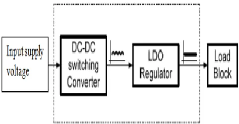
[image:1.597.315.556.291.416.2]The advantages of low dropout voltage regulator DC to DC regulators include the absence of switching noise, device size is small, and design simplicity is greater.
Fig -1: General LDO Regulator
The general LDO regulator is the Input supply voltage to given as the DC-DC Switching Converter is the analog waveform to the LDO Regulator is the Digital waveform to the load is Block.
2. CONVENTIONAL SINGLE STAGE AB- LDO
TOPOLOGIES
2.1Topology-1 (Differential Feedback Amplifier)
In operational Tran’s conductance amplifier is the voltage is applied across the inputs of the currents I1 and I2 become
© 2017, IRJET | Impact Factor value: 5.181 | ISO 9001:2008 Certified Journal
| Page 271
Fig -2: Differential feedback amplifier
2.2 Direct Feedback Amplifier
The direct feedback amplifier is used as a micro power buffer for large capacitive loads. The design is nearly the whole supply current is used to charge the load capacitor. The Fig -3 represents the amplifier. Split up in the amplifier is two symmetrical parts. the current of the branch is directly fed back to the tail current source in each input stage.
[image:2.597.44.285.121.378.2]Fig -3: Direct feedback amplifier
Fig -4: Single stage AB-LDO regulator in topology 1
Single stage AB-LDO regulator in topology 1 is the output current is given as,
I0=M.I2=M.I4
The M4 and Mp is mismatch of the current mirror is
ignored. To limited differential gain to increase I1 for the
ABL of the input offset is week mechanism.
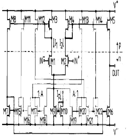
2.3 Topology- 2
The main differential pair transistors M1 and M2 generate an
error signal during normal negative feedback operation. The generated error signal is used to bias the tail current M0 effectively through the loop of transistors involving M6,
M7, M8, and M9. At steady state, there is no current flowing
into the capacitor Cc and it holds the required bias voltage at the gate of the tail-current source. Within the loop, when we go through the path1 whose transistors include M0, M1,
M3, and M6, we have a positive feedback loop. However, for
the path2 transistors M0, M2, M4, M7, M8, and M9, we have a
negative feedback loop. The load current is increases of I 0
and the error voltage is increased of I 1. When compared
[image:2.597.35.279.553.750.2]© 2017, IRJET | Impact Factor value: 5.181 | ISO 9001:2008 Certified Journal
| Page 272
Fig- 5: Single stage AB-LDO regulator topology 2
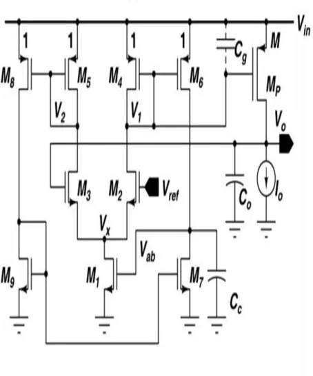
3. PROPOSED REGULATOR
Each of M4 and M5 are two parts, such as (M4a, M4b) and
(M5a, M5b). A cross-coupled configuration is the transistor
pair M4b–M5b is connected, as shown in Fig -6. The width of
the ratios between M4a–M4b and M5a–M5b pairs is 1: β, the
amplifier operation is β < 1. The cross-coupled pair is used for the multistage comparator design to the differential gain using a fixed-bias scheme is enhanced. In a single- stage configuration, when the cross coupled pair is combined with adaptive biasing, the operation is altered uniquely. The proposed ABL offers a few advantages. First, the variables of width ratio is A and β of the transistors and they are independent of I0. Due to these reasons are given
by, the regulator of dc operating point alters during large load change as the factor A • I2 changes it is proportionally
with I0. This factor is maintain the dc accuracy of V0 during
a large load change. A small error is present due to the inequality. A dc operating point of the differential operation is correct the error. Dc accuracy is increased in the regulator. I1 is the combination of the currents are
common mode as well as differential modes of operation, the magnitude of the latter one need not be very high in Topology-2.
Fig -6: Proposed regulator architecture
4. SIMULATION RESULT
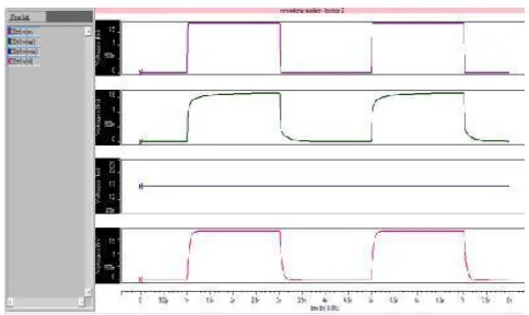
[image:3.597.310.536.122.344.2]Fig -7: Differential feedback amplifier in with capacitor
[image:3.597.48.275.131.404.2] [image:3.597.312.505.380.537.2] [image:3.597.311.524.578.712.2]© 2017, IRJET | Impact Factor value: 5.181 | ISO 9001:2008 Certified Journal
| Page 273
[image:4.597.307.572.154.363.2]Fig -9: Direct feedback amplifier in with capacitor
Fig -10: Direct feedback amplifier in without capacitor
Fig -11: Single stage with capacitor
Fig-12: Single stage without capacitor
Table –1: COMPARITIVE ANALYSIS
CIRCUIT RISE TIME
(pS)
FALL TIME (pS)
DELAY (nS)
POWER
(mW) PDP(pJ)
TOPOLOGY1 (WITH CAPACITOR)
0.25 0.26 2.03 4.46 9.07
(WITHOUT CAPACITOR)
0.19 0.21 2.03 4.35 8.84
TOPOLOGY 2(WITH CAPACITOR)
0.88 0.88 2.06 6.77 1.40
(WITHOUT
CAPACITOR) 0.19 0.21 2.03 4.71 9.58
PROPOSED (WITH CAPACITOR)
0.77 0.65 2.05 1.14 2.33
(WITHOUT CAPACITOR)
0.17 0.19 2.03 0.98 2.01
5. CONCLUSION
Conventional single stage adaptive biasing low dropout regulator and proposed regulator in with and without capacitor was designed and implemented by using 180nm CMOS technology and simulated using HSPICE simulator. Thus the regulator that consumes low power, low delay and power delay product was designed and rise time, fall time were calculated. Finally results were compared with the existing systems.
6. REFERENCES
[1] Ashis Marity, Amit Patra (2015),”Single- Stage Low Dropout Regulator with a Wide Dynamic Range for Generic Applications”, IEEE Transaction. Very Large Scale Integrator (VLSI) System.
[2] C.-H. Huang,Y.-T. Ma, and W.-C. Liao (2014), “Design of a
low-voltage low dropout regulator,” IEEE Transaction. Very Large Scale Integrator (VLSI) System, vol. 22, no.
6, pp. 1308–1313.
[3] M. G. Degrauwe, J. Rijmenants, E. A. Vittoz, and H. J. De
Man(1982), “Adaptive biasing CMOS amplifiers”, IEEE J. Solid-State Circuits, vol. 17, no. 3, pp.522–528.
[image:4.597.29.270.286.436.2] [image:4.597.29.270.464.603.2]© 2017, IRJET | Impact Factor value: 5.181 | ISO 9001:2008 Certified Journal
| Page 274
[5] A. Maity , A. Patra(2015), “Dynamic slew enhancement technique for improving transient response in an adaptively biased low-dropout regulator,” IEEE Trans. Circuits Syst. II, Exp. Briefs, vol. 62, no. 7, pp. 626–630. [6] D.J.Allstot(1982),“A precision variable-supply CMOS
comparator,” IEEE J. Solid-State Circuits, vol. 17, no.6, pp. 1080–1087.