Thesis by
Hossein Hashemi
In Partial Fulfillment of the Requirements for the Degree of
Doctor of Philosophy
California Institute of Technology Pasadena, California
2003
2003
Hossein Hashemi
In the past four years, perhaps the most important lesson I have learnt is that association with science in any form, getting a doctorate degree in my case, involves two parts. The first part, learning scientific facts and contributing to it, is something I have always enjoyed doing. Living a scientific life among an elite group of people in an exceptional place is the other part, and I did not have much of that experience before I came to Caltech. I was fortunate to enjoy the assistance, experience, support and friendship of many without whom I might not have been able finish this journey successfully. Here, I hope that I can express at least some part of my appreciation to all those who have helped my professional as well as personal life in the past few years.
First of all, I want to thank my academic advisor and my friend, Prof. Ali Hajimiri. What I learned from him goes well beyond pure academics. His high level of energy, intuition, wisdom, and efficiency, admittedly too difficult to follow for many, is a major contributor to one of the most successful groups in the field. I would like to acknowledge his personal assistance during my admission to Caltech and for helping me in adapting to the new environment. I would also like to thank him for giving me the opportunity to do the research I liked to do, and lastly for his major support for my future career. I look forward to many years of friendship and professional collaboration with him.
career.
Special thanks to my great colleagues and friends who had a substantial influence in my work at Caltech, especially Dr. Lawrence Cheung, Prof. Donhee Ham, Prof. Hui Wu, Behnam Analui and my office-mates (and dudes) Arun Natarajan and Xiang Guan who I’m sure will miss my loud presence in the room. The design of the multiple-antenna system in such a short time, deemed to be too risky by many of my friends, was only made possible by Xiang’s enthusiastic collaboration. Jim Buckwalter and Arun read many of my paper manuscripts, proposals, and thesis and gave me valuable comments on the material.
I am also thankful to many others in Caltech for their assistance in different stages of my Ph.D., Dr. Blythe Deckman, Milan Kovacevic, Dr. Matthew Morgan, Dai Lu, Dr. Taavi Hirvonen, Prof. Jim Rosenberg, Prof. Mike Delisio, Kent Potter, Niklas Wadefalk, Ann Shen, Abbas Komijani, Ehsan Afshari, Dr. Ichiro Aoki, Dr. Scott Kee, Roberto Aparicio, Sam Mandegaran, Chris White, Masoud Sharif, Amir Faraji-Dana, Florian Bohn, Rumi Chunara, Prof. Ali Jadbabaie, Naveed Near-Ansari, Dale Yee, Linda Dozsa, Carol Sosnowski, Heather Jackson, Parandeh Kia, and Jim Endrizzi.
I would like to thank the committee members in my candidacy exam. Prof. David Rutledge, Prof. Thomas McGill, Dr. Sander Weinreb, and Prof. Jehoshua Bruck gave me valuable feedback and insights during my presentation that I used in the later stages of my work.
I also want to thank my Ph.D. defense committee members, Dr. Sander Weinreb, Prof. Babak Hassibi, Prof. Yu-Chong Tai, and Prof. Oscar Painter, for their time.
Networking at Caltech, Caltech Center for Neuromorphic Systems Engineering (CNSE), National Science Foundation (NSF), and Xerox Corporation. I would also like to thank the von Brimer Foundation for the Outstanding Accomplishment Award, Analog Devices for the Outstanding Student Designer Award, and the Association of Professors and Scholars of Iranian Heritage (APISH) for the Young Scholar Award.
Solving difficult electrical engineering problems has always been the easy and fun part for me as long as my personal life is going smoothly. That’s why the following group of people are very special to me.
It’s only fair to start with my friend of 17 years, Sam, whose devotion to his friends is always exemplary. My room-mate and very good friend, Behnam, has been almost like a family member to me in the past couple of years. Amir and Helia are probably the only people with whom I shared many of my personal ups and downs over the past year. My cousin, Nikoo, has filled the void of my family in many ways and has also helped me a lot in proofreading the thesis manuscript. Many good friends were always present to lift my spirits and have a lot of fun over the past few years: Matthieu, Lisa, Arun, Jim, Donhee, Hui, Maryam, Fati, Ehsan, Abbas, Behroo, Abdi, Roya, Alireza, Ali, Leila, Lars, Ladan, Amir, Ichiro, Scott, Yazdan, Amirhossein, Javadagha and of course my close friends and running mates Taka and Jeremy and many others.
I would not be at this stage of my life had I not come across the single most influential person in my academic life, Prof. Ali Fotowat from Sharif University of Technology. The inspiration he has given me is indescribable in such a short space, but truly acknowledged.
person for what she does every day. Our new family member, Ali, is in many ways the brother I never had.
This thesis presents a unique view on radio systems that can simultaneously function at multiple frequency bands. These radios offer a higher data-rate and robustness in addition to the added functionality in the performance of wireless systems. Our treatment includes the definition of such novel radios, formulation of their singular characteristics, proposition for transceiver architectures, and invention of circuit blocks.
Various transceiver architectures for this new class of concurrent multi-band radios are proposed. The results for an integrated concurrent dual-band receiver operating at 2.4 GHz and 5.2 GHz frequency bands for wireless networking applications are presented. Meticulous frequency-planning results in a high level of integration and a low power design for the concurrent receiver. Several new circuit concepts including the concurrent multi-band low-noise amplifier are demonstrated in this design. A general class of these concurrent multi-band amplifiers is investigated with numerous implementations of integrated concurrent dual-band and triple-band amplifiers.
Contents
Acknowledgements iii Abstract vii
List of Figures xiv
List of Tables xxi
Chapter 1 Introduction 1
1.1 Motivation... 1
1.2 Organization... 3
Chapter 2 Multi-Band/Multi-Mode Radio Systems 5 2.1 Frequency Spectrum and Narrow-Band Communications ... 5
2.2 Why Multi-Band/Multi-Mode Radio?... 8
2.3 A Review of Existing Multi-Mode/Multi-Band Radio Architectures... 10
2.3.1 Multi-Band Receiver Architectures... 12
2.3.1.1 Heterodyne Architecture ... 13
2.3.1.2 Homodyne/Low-IF Architectures ... 13
2.3.1.3 Image-Reject Architectures ... 15
2.3.2 Multi-Band Transmitter Architectures... 16
2.3.2.1 Multi-Step Up-Conversion ... 16
2.3.2.2 Direct Up-Conversion ... 17
2.3.2.3 Up-Conversion via Direct VCO Modulation... 18
2.3.3 LO Generation in Multi-Band Transceivers ... 19
Chapter 3 Concurrent Multi-Band Radio 21
3.1 Benefits of Concurrency... 21
3.2 Concurrent Receiver Architectures ... 22
3.2.1 Parallel Single-Band Receivers ... 23
3.2.2 Parallel Receivers with a Wide-Band Front-End ... 24
3.2.3 Parallel Receivers with a Multi-Band Front-End ... 25
3.2.4 Multi-Band Sub-Sampling Receiver... 26
3.2.5 Direct Digitization (Digital Radio)... 28
3.3 A Concurrent Dual-Band Receiver ... 29
3.4 Concurrent Transmitter Architectures... 33
3.4.1 Scenario 1: Same Data for All Frequency Bands ... 34
3.4.2 Scenario 2: Different Data for Each Frequency Band ... 35
3.5 Adverse Effects and New Metrics in Concurrent Radios... 36
3.6 Summary... 39
Chapter 4 Concurrent Multi-Band Amplifiers 40 4.1 A Review of Single-Band LNA Design Issues... 41
4.1.1 Technology... 41
4.1.2 Topology ... 42
4.2 Concurrent Multi-Band Low-Noise Amplifiers... 44
4.2.1 Concurrent Multi-Band LNA Design Methodology ... 45
4.2.1.1 General Amplifier in Common-Source Configuration... 46
4.2.1.2 Input Matching... 47
4.2.1.3 Noise Matching ... 49
4.2.1.4 Load Circuit, Output Matching and Gain... 59
4.2.1.5 Practical Considerations ... 60
4.2.2 Concurrent LNA Design Examples and Measurement Results ... 64
4.2.2.1 A High-Performance Concurrent Dual-Band LNA ... 64
4.2.2.2 A Fully Integrated Concurrent Dual-Band Amplifier ... 69
4.2.2.3 Fully Integrated Concurrent Triple-Band Amplifiers ... 72
4.3 Multi-Band Power Amplifiers ... 74
Chapter 5 An Experimental Concurrent Dual-Band Receiver 77
5.1 Top-Level Radio Design ... 77
5.1.1 WLAN Standards and System Analysis ... 78
5.1.2 Receiver Architecture ... 81
5.2 Receiver Building Blocks ... 86
5.2.1 Concurrent Dual-Band LNA ... 86
5.2.2 Concurrent Dual-Band RF Mixer ... 88
5.2.3 IF Image-Rejection Mixers ... 88
5.2.4 Local Oscillator Frequency Generation ... 89
5.2.5 Analog Frequency Dividers ... 91
5.3 Experimental Results... 97
5.4 Summary... 102
Chapter 6 Oscillators with Multi-Band Resonators 103 6.1 Time-Domain Response of Multi-Frequency Oscillators ... 104
6.1.1 A Brief Overview of Second-Order Oscillators ... 105
6.1.2 A Brief Review of Previous Work ... 108
6.1.3 Problem Formulation of a Fourth-Order System ... 110
6.1.4 Multi-Frequency Oscillations in Fourth-Order System ... 115
6.1.5 A Few Potential Applications of Multi-Frequency Oscillations .... 122
6.2 Phase-Noise of Oscillators with a Generalized Resonator Structure ... 123
6.2.1 Resonator Quality Factor ... 125
6.2.1.1 Resonator Quality Factor without Coupling Terms ... 128
6.2.1.2 Resonator Quality Factor Including Coupling Terms ... 129
6.2.1.3 Useful Expressions for Resonator Quality Factor ... 131
6.2.2 Phase Noise ... 134
6.2.3 Circuit Examples ... 138
6.3 Summary... 143
Chapter 7 A Multiple-Antenna Phased-Array Radio 144 7.1 Brief Overview of Multiple-Antenna Systems ... 145
7.1.1.1 Receiver Diversity... 147
7.1.1.2 Transmitter Diversity ... 148
7.1.2 Phased Array ... 149
7.1.2.1 Phase Shift vs. Time Delay... 154
7.2 Phased-Array Radio Architectures... 155
7.2.1 Phase Shifting and Signal Combining in Signal Path... 155
7.2.2 Phase Shifting in Local-Oscillator Path... 156
7.2.3 Digital Array Implementation ... 157
7.3 A 24 GHz Phased-Array Radio... 159
7.3.1 Receiver Architecture ... 160
7.3.2 Receiver Building Blocks ... 164
7.3.2.1 RF Front-End ... 164
7.3.2.2 IF Circuitry47... 165
7.3.2.3 Generating Multiple Phases of Local Oscillator... 165
7.3.2.4 A 19 GHz Multi-Phase Voltage Controlled Oscillator ... 170
7.3.2.5 Phase-Selection Circuitry ... 172
7.3.2.6 LO Phase-Distribution Network ... 175
7.3.3 Measurement Results of the Implemented Receiver ... 177
7.4 Summary... 190
Chapter 8 Conclusion 192 8.1 Summary... 192
8.2 Recommendations for Future Work... 193
Appendix A General Small-Signal Expressions for a Common-Source Amplifier 195 Appendix B Noise Source Transformations 197 Appendix C Nonlinear Differential Equation of a Fourth-Order System with
Multiple Sources of Loss 198
List of Figures
Figure 2.1: Simplified illustration of single-band radios (a) time-duplex (b) full-duplex ... 11
Figure 2.2: Illustration of cross-talk caused by the image signal in the receiver... 12
Figure 2.3: A multi-band / multi-mode receiver based on Heterodyne architecture [6] ... 13
Figure 2.4: A direct-conversion multi-band receiver for mobile-phone applications [15] .. 15
Figure 2.5: Dual-band receiver based on Weaver’s image-rejection scheme [9] ... 16
Figure 2.6: Dual-band transmitter using dual up-conversion for CDMA standards [10] .... 17
Figure 2.7: Dual-band direct-conversion transmitter for CDMA standards [14] ... 18
Figure 2.8: Dual-band transmitter based on direct-modulation of VCO frequency [15] ... 19
Figure 3.1: Concurrent receiver implementations using multiple parallel single-band, receivers in (a) heterodyne (b) direct down-conversion architectures... 24
Figure 3.2: Concurrent receiver implementation using a wide-band front-end in (a) heterodyne (b) direct down-conversion architectures... 25
Figure 3.3: Concurrent receiver implementation using a multi-band front-end in (a) heterodyne (b) direct down-conversion architectures... 26
Figure 3.4: Frequency domain representation of down-conversion using bandpass subsampling... 27
Figure 3.5: Frequency domain representation of multi-band subsampling ... 28
Figure 3.6: Generic architecture of a direct digitization radio... 29
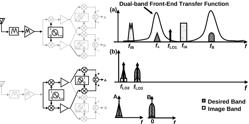
Figure 3.7: Evolution process of two parallel receivers to a concurrent dual-band receiver 30 Figure 3.8: Concurrent dual-band receiver architecture... 31
Figure 3.9: Operation principle of the proposed concurrent dual-band receiver in frequency domain... 33
Figure 3.10: Proposed concurrent dual-band transmitter in scenario 1... 34
Figure 3.11: Proposed concurrent dual-band transmitter in scenario 2... 35
Figure 3.13: Depiction of (n+m) order cross-band intermodulation ... 37 Figure 3.14: Illustration of reciprocal mixing caused by local oscillator phase-noise... 38 Figure 4.1: Commonly used single-band CMOS LNAs (a) gate (b)
common-source with inductive degeneration ... 43 Figure 4.2: Generic schematic of existing multi-band amplifiers... 45 Figure 4.3: General model for a single-stage amplifier in common-source configuration. . 46 Figure 4.4: General representation of any noisy 2-port (a) and its equivalent circuit (b) .... 50 Figure 4.5: (a) NF and ft for a bipolar transistor with τF=3.67ps (b) Different noise
contributions to the total NF from (4.16) (NF numbers for 5.8 GHz)... 56 Figure 4.6: NF of a 0.18 µm CMOS transistor at 5.8 GHz with finger width of 2 µm vs. nf and Vod... 57 Figure 4.7: (a) NF, fT of a 20 x 2.5 µ / 0.18 µ CMOS transistor. (b) ID, gm, gd0 of the
transistor. (c) Different noise contributions to the total NF from (4.16) (NF numbers at 5.8 GHz)... 58 Figure 4.8: Basic illustration revealing that the combination of multi-frequency signals
requires a more linear amplifier design ... 61 Figure 4.9: Simulated return-loss of a dual-band (dotted-curve) and a triple-band
(solid-curve) input matching circuitry (a) Qind=100 (b) Qind=10... 62
Figure 4.10: (a) Simulated results comparing the value of triple-band (solid-curve), dual-band (bold dotted-curve) and single-dual-band (dotted-curve) impedance functions (b) Typical curve for the quality factor of on-chip spiral inductors that is used to generate impedance function curves... 63 Figure 4.11: Concurrent dual-band CMOS LNA (biasing circuitry not shown) ... 65 Figure 4.12: Voltage-gain and S11 in concurrent dual-band CMOS LNA of Figure 4.11.... 66
Figure 4.13: Chip micrograph for the concurrent dual-band CMOS LNA in Figure 4.11.. 67 Figure 4.14: Schematic and layout of an integrated dual-band CMOS amplifier... 70 Figure 4.15: Voltage-gain and return-loss of concurrent dual-band amplifier of Figure 4.14
... 71 Figure 4.16: Schematic and layout of an integrated triple-band CMOS amplifier ... 73 Figure 4.17: Voltage-gain and return-loss of concurrent triple-band amplifiers using the
Figure 5.1: Complete schematic of the fully integrated concurrent dual-band receiver ... 82
Figure 5.2: Frequency planning of the concurrent dual-band receiver in Figure 5.1... 84
Figure 5.3: Simplified schematic of the concurrent dual-band LNA... 87
Figure 5.4: Simplified schematic of the dual-band RF mixer... 88
Figure 5.5: Simplified schematic of IF one pair of image-rejection mixers... 89
Figure 5.6: Simplified schematic of the 6.3 GHz PLL 23... 90
Figure 5.7: (a) Two-stage stagger-tuned poly-phase structure for LO quadrature generation; (b) its frequency response in complex domain... 91
Figure 5.8: Simplified schematic of the divide-by-two ILFD in [105] and [106] ... 93
Figure 5.9: Simplified schematic of the proposed divide-by-three ILFD ... 94
Figure 5.10: Divide-by-three principle of operation under no input signal at (a) fundamental oscillation frequency (b) odd harmonics of oscillation frequency (c) even harmonics of oscillation frequency... 94
Figure 5.11: Simulated results of the ILFD in Figure 5.9 with no injected input power and for fosc=2.1 GHz: (a) frequency contents of current in M3,4 , (b) frequency contents of current in the LC series branch of Ls and Cs... 95
Figure 5.12: Simulated locking-range of the implemented ILFD-based 6.3 GHz divide-by-three versus divider’s current consumption ... 96
Figure 5.13: Die micrograph of the first version of concurrent receiver (off-chip LO)... 97
Figure 5.14: Die micrograph of the second version of concurrent receiver (fully integrated) ... 98
Figure 5.15: Test board to measure the performance of concurrent receiver ... 99
Figure 5.16: Typical measurement setup for the concurrent receiver... 99
Figure 5.17: Measured gain of the concurrent receiver at two bands of interest... 100
Figure 5.18: Large-signal gain characteristic of the receiver at the higher frequency band ... 100
Figure 6.1: A simple model for a second-order electrical oscillator... 105
Figure 6.2: Cross-coupled pair oscillator with a simple second order LC resonator and the plot of resonator’s impedance magnitude ... 107
Figure 6.3. Triode oscillator with two degrees of freedom analyzed in [121] ... 109
Figure 6.5: Impedance magnitude of the fourth-order resonator of Figure 6.4 when ω s is
closer to: (a) ω 2, (b) ω 1... 111
Figure 6.6: Cross-coupled pair oscillator with the fourth-order dual-resonance tank depicted in Figure 6.4 ... 115 Figure 6.7: Graphical representation of the stability of multiple solutions to (6.14) for a 3rd
order power expansion of the nonlinear voltage-current characteristic... 119 Figure 6.8: Simulation results showing asynchronous oscillations in Figure 6.6... 121 Figure 6.9: Dual-band Colpitts-type oscillator generating synchronous oscillations ... 122 Figure 6.10: A potential single-chain concurrent receiver using a multi-band oscillator .. 123 Figure 6.11: General model of a negative-resistance oscillator with a resonator... 124 Figure 6.12: Frequency spectrum magnitude of a sixth-order and a second-order resonator (a sixth-order resonator structure is shown in Figure 6.13) ... 127 Figure 6.13: A sixth-order triple-band resonator ... 127 Figure 6.14: Two examples of resonators that use coupled inductors: (a) Quality factor
increases, since coupling energy adds to total stored energy (i1 and i2 in-phase). (b) Quality factor decreases, since coupling energy subtracts from total stored energy (i1 and i2 out-of-phase)... 131 Figure 6.15: Impedance definition of a one-port network... 132 Figure 6.16: Illustration of phase-noise definition per unit bandwidth... 135 Figure 6.17: Cross-coupled pair oscillator with a fourth-order resonator implemented using transformers... 139 Figure 6.18: Impedance magnitude of the higher-order resonators (solid-curves) compared to the second-order LC resonator of Figure 6.2 (dotted curves) (a) fourth-order resonator used in oscillator of Figure 6.6 (b) sixth-order resonator used in oscillator of Figure 6.13 (c) fourth-order transformer-based resonator used in oscillator of Figure 6.17 [Coupling-factor k=0.9 is assumed in this figure] ... 140 Figure 6.19: A proposed combination of three coupled inductors in a resonator structure to achieve a higher energy-based definition of quality factor that results in an enhanced phase-noise performance if inserted in an oscillator core... 142 Figure 6.20: Simulated phase-noise of three cross-coupled oscillators at 5 GHz having a
6.19. Oscillation amplitude is 0.830 V, 0.805 V and 0.795 V for these cases,
respectively... 142
Figure 7.1: Wireless communication channels (a) line-of-sight (b) multi-path fading... 145
Figure 7.2: Narrower antenna beams using multiple-antenna elements... 146
Figure 7.3: Characteristic of a received signal envelope in a typical fading channel (courtesy of [137]) ... 147
Figure 7.4: Simplified scheme of a maximal ratio combining receiver using spatial diversity ... 148
Figure 7.5: Illustration of a MIMO system and space-time coding at the transmitter ... 149
Figure 7.6: Phased-array concept (gain control block is only necessary when controlling multiple peaks and nulls is desired)... 151
Figure 7.7: Schematic of a phased-array receiver used for SNR calculations ... 153
Figure 7.8: Phased-array receiver using signal-path (RF or IF) phase shifting... 156
Figure 7.9: Phased-array receiver using LO phase shifting... 157
Figure 7.10: Phased-array receiver using baseband signal processing (digital array) ... 158
Figure 7.11: Block-diagram schematic of the 24 GHz phased-array receiver... 162
Figure 7.12: Relative gain of the array with 4-bit discrete phase shifting ... 163
Figure 7.13: Schematic of the 24 GHz front-end consisting of a 2-stage LNA and Gilbert-type mixers in each channel ... 164
Figure 7.14: Schematic of the 4.8 GHz IF stage consisting of IF amplifiers and double-balanced Gilbert-type mixers ... 165
Figure 7.15: A first-order passive all-pass filter and its phase transfer-function... 166
Figure 7.16: Broadband phase shifting using all-pass functions ... 167
Figure 7.17: A generic phase-interpolator and a vector-diagram for sinusoid input signals ... 168
Figure 7.18: An array of coupled oscillators for multiple phase generation ... 169
Figure 7.19: Multi-phase oscillators in ring configuration (a) using delay elements (b) traveling wave oscillator with a transmission line ... 170
Figure 7.20: Schematic of the 19 GHz VCO that generates 16 phases of LO... 171
Figure 7.22: Schematic of LO phase selection circuitry for each path (biasing not shown). (a) selecting one of 8 oscillator output pairs; (b) dummy array to maintain constant
loading for all phases; (c) sign selector ... 174
Figure 7.23: Array response with ±2.5° of mismatch in LO phase distribution (thick line) compared to the ideal case (thin line) for 8-path receiver ... 175
Figure 7.24: Tree structure used for a symmetric distribution of 16 LO phases ... 176
Figure 7.25: Die micrograph of the 24 GHz fully integrated phased-array receiver ... 177
Figure 7.26: Oscillation frequency vs. varactors’ control voltage ... 178
Figure 7.27: Oscillator output spectrum and phase-noise at 18.70 GHz... 179
Figure 7.28: PFN of various oscillators... 180
Figure 7.29: Measurement setup for 4-channel array characterization ... 181
Figure 7.30: Close-up of the measured chip mounted on a brass substrate... 182
Figure 7.31: Input return-loss of the receiver ... 183
Figure 7.32: Receiver small-signal transfer function for the main and image signals... 184
Figure 7.33: Large-signal response of the receiver at 23 GHz input frequency ... 184
Figure 7.34: Intermodulation test of the receiver (a) Typical output spectrum when two large-signal input tones are applied (b) Results of two-tone test ... 185
Figure 7.35: Received pattern measurements of the phased-array system with two operating paths ... 186
Figure 7.36: Simulated beam-width comparison of the 8-channel phased array with the case when only 2 paths are working... 187
Figure 7.37: Received pattern measurements of the phased-array system with four operating paths compared with theory ... 187
Figure A.1: Equivalent small-signal model for the generic amplifier of Figure 4.3... 195
Figure B.2: Illustration of noise source transformation in (a) series (b) parallel cases... 197
Figure C.3: A second-order oscillator model with multiple sources of loss ... 198
Figure E.4: Simplified model used to calculate ISF of an oscillator with a fourth-order resonator in Figure 6.6 ... 205
List of Tables
Table 2.1: Selected portions of FCC-allocated frequency-spectra for narrow-band
communications... 7
Table 2.2: Selectivity of selected narrow-band communication receiver systems ... 8
Table 2.3: Today’s predominant mobile-phone standards ... 9
Table 4.1: Comparison of Vchar, and ωT in different sub-micron CMOS processes... 54
Table 4.2: Performance summary of the concurrent dual-band CMOS LNA ... 68
Table 4.3: Comparison of existing single-band CMOS LNAs and the concurrent multi-band LNA at the same frequency bands (S-band and C-band) ... 68
Table 5.1: Summary of a few wireless networking standards at 2.4 GHz and 5 GHz... 80
Table 5.2: Receiver target numbers for standards in Table 5.1 ... 81
Table 5.3: Concurrent receiver frequency planning that uses only divide-by-two ... 84
Table 5.4: Concurrent receiver frequency planning that exploits by-three and divide-by-two circuit blocks ... 85
Table 5.5: Component values of the implemented divide-by-three ILFDs in Figure 5.9 (a) 6.3 GHz to 2.1 GHz divider (b) 2.1 GHz to 0.7 GHz divider ... 96
Table 5.6: Concurrent dual-band receiver performance summary ... 101
Table 6.1: Quality factor comparison for different resonator structures ... 141
Chapter 1
Introduction
Achieving the highest possible performance of wireless devices, irrespective of cost, was the primary focus of early radio engineers. The advent of commodity wireless appliances has gradually shifted the emphasis towards the most affordable solution. With the increase in demand, and rapid improvements in the semiconductor technology, the cost of wireless devices has considerably reduced. Additionally, the complexity of operations performed on Integrated Circuits (ICs) has grown exponentially [1]. In this environment of decreasing cost and increasing complexity, acquiring more functionality and flexibility is the best objective for future integrated wireless devices. This thesis presents such an approach towards increased functionality and performance of integrated wireless systems.
1.1
Motivation
As a result of the shared medium in wireless communications, the valuable frequency-spectrum has been divided to serve a diverse range of applications. Conventionally, wireless devices operate at a frequency band allocated for a particular application. Since received signals from other wireless devices act as undesirable interference, radio transceivers are often designed for a narrow frequency bandwidth. The limited operation bandwidth of these systems makes them incapable of functioning at frequency bands other than their own.
example of such a multi-mode system is the common household radio that has to cover, at least, the AM and FM frequency bands. Additionally, radio transceivers that can be used for more than one application are of a great interest. Multi-band mobile phone terminals with capability of wireless connection to the Internet are examples of the latter case.
In this thesis, we will present a unique view on multi-mode and multi-band radio systems that can simultaneously function at multiple frequency bands. These novel radios offer a higher data-rate, robustness, and improvement, in addition to the added functionality, in the performance of wireless systems. Our treatment comprises of the definition of such novel radios, formulation of their particular characteristics, proposals for potential transceiver architectures, and invention of circuit blocks. Throughout the discussions, our theoretical findings are verified with experimental implementations of the developed concepts.
The performance of wireless systems can be further enhanced by exploiting the spatial properties of the electromagnetic wave. The combination of signals extracted from (or inserted to) different physical points of a propagated wave increases the energy of the signal. Using multiple-antenna systems is a natural way of collecting and generating signal energy at different points in space in order to achieve higher data-rate wireless communications.
With the goal of demonstrating a significant improvement in the performance of traditional wireless devices, and in order to bridge the scientific gap between the conventional integrated-circuit designs and microwave techniques, the design and implementation of an ultra high-frequency multiple antenna radio system will be presented. Of particular interest is the integration of the complete system on a commercially available silicon technology that paves the way for a low-cost alternative for high-performance wireless communication schemes.
1.2
Organization
After describing the traditional narrow-band radio design from a historical basis, the motivations behind advancing to multi-band and multi-mode wireless systems will be explained in Chapter 2. We will then present a brief overview of existing multi-band and multi-mode radio architectures.
Traditional multi-band transceivers that will be discussed in Chapter 2 are incapable of a simultaneous operation at multiple frequency bands. In Chapter 3 we will introduce the new concept of concurrent multi-band radios and will show their benefits in many cases. Receiver and transmitter architectures for this new class of radios will be revealed, many of which relying on the novel building blocks that will be described in detail throughout this thesis. Furthermore, upcoming challenges particular to concurrent multi-band radios, as well as new metrics for characterizing those systems, will be discussed.
Chapter 4 covers the theory, design, and implementation of concurrent multi-band amplifiers that serve as key parts in concurrent radio architectures. A general class of concurrent low-noise amplifiers that can achieve minimum noise-figure, input matching, and narrow-band gain at multiple frequency bands are introduced and analyzed comprehensively. Based on the results of our general treatment, a number of integrated concurrent dual- and triple-band amplifiers are designed and implemented. The validity of our theoretical predictions is confirmed through successful measurements of the concurrent amplifiers.
In Chapter 6, we will present a theoretical treatment of multi-frequency oscillators. Nonlinear oscillators with multi-band resonator structures, under certain conditions, are capable of generating tone at distinct frequencies. A thorough analysis of one such oscillator with a dual-band resonator is carried out, providing the conditions of simultaneous multi-frequency oscillations. In the second part of this chapter, the phase-noise of negative-resistance oscillators with general resonator structures is addressed. By providing a link between the stored and dissipated energies of a network and its associated circuit parameters, useful interpretations of resonator quality factor are derived. With the aid of this analysis and the previously developed phase-noise models, dependencies of phase-noise to the resonator structure are derived. Inspired from our theoretical findings, enhanced resonators with a higher quality factor that can provide a superior oscillator phase-noise are proposed.
In Chapter 7, integrated multiple-antenna radios in phased-array configuration are investigated. A brief overview of different types of multiple-antenna systems is presented in order to demonstrate their effectiveness in high data-rate and reliable wireless communication schemes. A comparison of various architectures for such systems is followed by a practical design of an ultra high-frequency phased-array radio receiver on a conventional silicon technology. The successful implementation of this radio is achieved by a collection of innovative integrated-circuit and microwave techniques in addition to simulation, modeling, and characterization of such high-frequency designs.
Chapter 2
Multi-Band/Multi-Mode Radio Systems
Electromagnetic waves are used for wireless transmission of information in a variety of applications. The majority of radio transceivers are designed for a particular purpose; for example, a TV tuner converts the received electromagnetic wave into picture and sound, while a mobile phone uses these waves for wireless voice and data communications. Often, these wireless devices have different modes of operation. For instance, one can use a single radio tuner to listen to either AM or FM radio broadcast stations. The multi-standard mobile phone terminal is a more recent illustration of a multi-mode radio. Radio systems with different modes of operation are the subject of this chapter. After explaining the fundamental reason behind the historical application-specific radio design, motivations for evolving to multi-mode radios will be discussed. A few instances of existing multi-mode radio architectures will be followed by the discussion of the role of such systems in the future of wireless communications.
2.1
Frequency Spectrum and Narrow-Band Communications
the common medium for transmitting and receiving signals using any of the multiple access schemes such as Time-Division (TDMA), Frequency-Division (FDMA), or Code-Division (CDMA) [3].
At the same time, this common medium has to be used for numerous applications that are very dissimilar in nature. For instance, a broadcasting TV station sends a powerful signal in all directions so that the received signal quality in the entire neighborhood is sufficiently high. Meanwhile, a satellite receiver extracts its intended data of a tiny signal emitted from a distant location. Consequently, a government agency called the Federal Communications Commission, FCC, was established in 1934 and is responsible for allocating and regulating radio communications in the United States. Similar regulating agencies have been established elsewhere in the world. In order to allow different applications to coexist and function simultaneously, the frequency-spectrum has been divided into numerous narrow sectors, each allocated for a particular application. A very limited selection of FCC frequency-allocations from 1 MHz to 100 GHz is shown in Table 2.1. The distinction in the nature of these applications has resulted in various restrictions such as maximum allowable emitted power or modulation type for each of these narrow frequency bands. A number of often conflicting factors, many of them historical, economical, and political, have been considered in the frequency spectrum planning. A number of the common trade-offs considered among data rate, range, and frequency of operation are briefly described below.
Based on Shannon’s theorem, the maximum data-rate of a communication channel, known as channel capacity, C, is related to the frequency bandwidth of the channel, BW, and the signal-to-noise ratio, SNR in the following manner [2]:
) 1
( log
. 2 SNR
BW
C = + (2.1)
based on the overly simplistic and limited discussion above, we can appreciate the subtlety in the planning of the frequency spectrum.
Table 2.1: Selected portions of FCC-allocated frequency-spectra for narrow-band communications
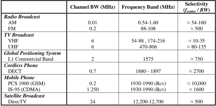
As a result of the frequency allocation (e.g., Table 2.1), the majority of communications though air is essentially narrow-band1 where the ratio of center frequency of the utilized band to its bandwidth is often between 100 and 10,000 (Table 2.2). In order to
1 MHz 1 GHz 10 GHz 100 GHz
Broadcast
FM Radio 88-108
Television 54-88 , 174-216 , 470-608 , 614-806
Cellular Telephone 824-849 , 869-894
Personal Communications
Broadband 1.850–1.990
Narrowband 901-902 , 930-931 , 940-941
Unlicensed 1.910-1.930 , 2.390-2.400
RFID (Radio ID Devices) 902-928 2.400-2.500
Industrial, Scientific & Medical
(ISM) 40.66-40.7 , 902-928 2.45-2.50 , 5.725-5.875 24-24.25 , 59-64
Unlicensed National Information
Infrastructure (UNII) 5-5.35 , 5.65-5.85
Paging and Radiotelephone Services 35 , 43 , 152 , 158 , 454-455 , 459-460 , 929-930 , 931-932 Local Multipoint Distribution Service
(LMDS) 27.5-29.5 , 31-31.3
Satellite Services
Direct Broadcast / Direct to Home 11.7-12.2 , 12.2-12.7 , 17.3-17.7 Digital Audio Radio Service (DARS) 2.320-2.345
Global Positioning System (GPS) 1.215-1.240 , 1.35-1.40 , 1.559-1.610
Vehicle Anti-Collision Radar/
communicate effectively and achieve a high performance, every radio transceiver is highly selective around a particular frequency band and rejects all the other present signals. Several radio architectures such as heterodyne, homodyne and regenerative can achieve the necessary selectivity at high frequencies. However, due to the selective nature of narrow-band communications and the distinction in specifications of various systems such as bandwidth, modulation type, power levels, etc., none of the conventional radio transceivers is capable of supporting multiple applications, simultaneously.
[image:29.612.121.535.270.474.2]The issue of narrow-band radios that are able to function for multiple applications is the topic of next section.
Table 2.2: Selectivity of selected narrow-band communication receiver systems
2.2
Why Multi-Band/Multi-Mode Radio?
As previously mentioned, narrow-band communication and spectrum allocation have enabled the coexistence of multiple standards and applications in an efficient fashion. Accordingly, every wireless radio is designed and optimized to operate for a particular
application at its allocated frequency band. At the same time, oftentimes various frequency
1
Recently, wide-band communication for low-power, short-range and high data-rate commercial applications is receiving more attention [4].
Channel BW (MHz) Frequency Band (MHz) Selectivity
(fcenter / BW) Radio Broadcast
AM 0.01 0.54-1.60 ≈ 54-160
FM 0.2 88-108 ≈ 500
TV Broadcast
VHF 6 54-88 , 174-216 ≈ 10-35
UHF 6 470-806 ≈ 80-135
Global Positioning System
L1 Commercial Band 2 1575 ≈ 750
Cordless Phone
DECT 0.7 1880 - 1897 ≈ 2700
Mobile Phone
PCS 1900 (GSM) 0.2 1930-1990 (Rcv) ≈ 10,000
IS-95 (CDMA) 1.250 1930-1990 (Rcv) ≈ 1600
Satellite Broadcast
bands with distinct specifications such as modulation type and power emission ratings are allocated for the same application. Mobile phone communication is a common case where multiple frequency bands with a variety of specifications are used. Due to the diversity of these radio specifications at different frequency bands, a conventional mobile phone terminal can only operate under one standard at a particular frequency band. Some of today’s mobile-phone standards are listed in Table 2.3, as a demonstration of this concept2.
Table 2.3: Today’s predominant mobile-phone standards
These diverse sets of standards have prompted the design and manufacturing of multi-standard mobile phone terminals. These multi-mode systems can operate at different standards in various regions of the world and eliminate the need to carry more than one phone while traveling.
2
The brief description of mobile-phone standards is only to demonstrate one instance of an application with multiple designated frequency bands. These examples do not limit our general discussions and treatments of the multi-mode and multi-band wireless systems.
GSM CDMA
E-GSM DCS1800
(PCS1900) IS-95 W-CDMA
Downlink Band 925-960 MHz 1805-1880 MHz (1930-1990)
869-894 MHz
(1930-1990) 2110-2170 MHz
Uplink Band 880-915 MHz 1710-1785 MHz
(1850-1910)
824-849 MHz
(1850-1890) 1920-1980 MHz
Channel Bandwidth 200 kHz 1.25 MHz 1.25/5/10/20 MHz
Downlink Data-Rate 22.8 kbit/s 1.2/2.4/4.8/9.6/14.4 kbit/s 2n kbit/s (n=5..11) Uplink Data-Rate 22.8 kbit/s 1.2/2.4/4.8/9.6/14.4 kbit/s 2n kbit/s (n=4..10)
Modulation GMSK BPSK QPSK
Multiple Access TDMA Direct Sequence CDMA
Duplexing FDD FDD
Maximum Output
Power 30 / 33 dBm 24 dBm 23-30 dBm
GMSK: Gaussian Minimum Phase Keying TDMA: Time Domain Multiple Access
QPSK: Quadrature Phase Shift Keying CDMA: Code Division Multiple Access
Perhaps the most common multi-mode system is the common household radio receiver itself, which usually receives both AM and FM broadcast signals, one at a time. In addition to radios and mobile-phones, there are other types of applications where multi-mode systems have received a lot of attention. Wireless networking is another example of numerous standards prompting the creation of multi-mode transceivers. Different aspects for wireless networking applications will be discussed in Chapter 5.
There is also an increasing interest in radio systems that support more than one application. For instance, adding wireless networking ability to the existing mobile phone terminals might be realized in the near future. Radio architectures for mobile-phones with global-positioning-system (GPS) capability have already been discussed in the literature [6]. Such multi-mode systems that simultaneously support various applications operating at different frequency bands are the subject of Chapter 3.
There is a subtle distinction between multi-mode and multi-band in existing publications. Multi-band systems operate for several standards occupying different frequency bands. For instance, a dual-band GSM mobile-phone usually refers to a system that can operate at 900 GHz and 1800 GHz frequency bands (refer to Table 2.3). More generally, multi-mode transceivers can function for various standards residing in the same frequency band or in disjointed ones3.
In the next section, some of the proposed and implemented transceiver architectures for multi-band systems, mostly in mobile-phone and wireless networking applications, are briefly reviewed.
2.3
A Review of Existing Multi-Mode/Multi-Band Radio Architectures
A complete radio transceiver consists of two separate paths, radio receiver and radio transmitter (Figure 2.1). In the receiver chain, the collected signal from the antenna is amplified, filtered and down-converted in frequency for reliable detection and demodulation in the following signal-processing stages. In the transmitter section, the modulated signal has to be up-converted to the appropriate radio frequency and amplified
3
before entering the antenna for proper propagation. Therefore, sections that are closer to the antenna operate at the higher frequency in the transceiver chain. In particular, the first active block in the receiver, a low-noise amplifier (LNA), increases the level of the received signal without adding a significant amount of noise. On the transmitter side, a power amplifier (PA) provides the desirable amount of signal energy to the antenna.
Figure 2.1: Simplified illustration of single-band radios (a) time-duplex (b) full-duplex
Regardless of the radio architecture, the connection of the transceiver’s front-end to the antenna is a function of the duplexing method. Both the output of power-amplifier (PA) and the input of low-noise amplifier (LNA) have to be connected to the antenna with a high isolation between them. The isolation is required to protect the sensitive receiver front-end circuitry from the large signal levels at the PA output and to minimize the leakage of the transmitted signal energy to the receiver path. In full-duplex systems, such as CDMA standard in mobile-phones, where the receiver and transmitter are simultaneously on, bulky duplex filters that separate receive and transmit bands are usually unavoidable (Figure 2.1 b). In time-duplex schemes such as the GSM standard for mobile-phones, there is a time gap between receive and transmit frames. In these schemes, a transmit/receive (TR) switch, followed by bulky surface-acoustic-wave (SAW) filters in receiver chain in many cases, separates the antenna connection to each path (Figure 2.1 a). For multi-band systems, more duplexers, TR switches, and SAW filters are needed to accommodate all of the desired frequency bands.
Tx/Rx Switch
LNA
PA
Demodulator
Modulator Frequency
Down-Converter
Frequency Up-Converter BPF
Duplexer LNA
PA
Demodulator
Modulator Frequency
Down-Converter
Frequency Up-Converter
2.3.1
Multi-Band Receiver Architectures
In practice, the high selectivity required in narrow-band communications (Table 2.2) can hardly be achieved with any practical filter at radio frequencies. Therefore, the desired selectivity is often achieved in multiple stages. The carrier frequency of the received signal is lowered in one or more steps allowing for filtering and demodulation at lower frequencies. In a common process known as down-conversion, the carrier frequency of a modulated signal can be reduced by multiplying (or mixing) it with a constant tone signal of a local oscillator (LO)4. Unfortunately, in a multiplier, the image of the main signal with respect to the LO frequency is down-converted along with the main signal to the same frequency causing an unwanted cross-talk (Figure 2.2). Usually, distinct receiver architectures vary in the number of down-conversion stages, the method to remove the unwanted image signal, as well as the choice of placement and value of gain and filtering stages.
Figure 2.2: Illustration of cross-talk caused by the image signal in the receiver
Most of today’s wireless receivers use any of these general architectures: heterodyne, homodyne, low-IF, and image-rejection receivers such as the ones originally proposed by Weaver [8] or Hartley [7]. Similarly, all these architectures have been employed in the multi-band receivers for various applications. In the following sections, advantages and disadvantages of each of these architectures for multi-band and multi-mode systems are briefly discussed.
4
Similarly, the carrier frequency can be increased in a mixing process (up-conversion). LO
fLO
-fLO
desired signal image signal
fRF
-fRF -fRF+fLO fRF-fLO
|fRF-fLO|
2.3.1.1
Heterodyne Architecture
Heterodyne receivers achieve a large selectivity by down-converting the received RF signal in multiple steps (usually two), and by extensive filtering at each intermediate-frequency (IF) section before converting the analog baseband signal to a digital one for demodulation and further signal processing. Filtering at RF and IF stages is usually achieved via external SAW filters that attenuate the energy at the image frequency band for reduced cross-talk. In a multi-band heterodyne system, there will be a larger number of external image-rejection filters resulting in a larger footprint, higher power consumption, and a higher overall cost for the system. A simplified schematic of a triple-band receiver for CDMA phone standards integrated with GPS capability (quad-mode radio) that uses a heterodyne architecture is shown in Figure 2.3 ([6]).
Figure 2.3: A multi-band / multi-mode receiver based on Heterodyne architecture [6]
2.3.1.2
Homodyne/Low-IF Architectures
The cross-talk caused by the image signal can also be eliminated if a pair of multipliers with in-phase and quadrature-phase LO signals are used in the down-version stage.
Homodyne (also known as zero-IF or direct-conversion) receivers perform the radio frequency down-conversion in only one step using a pair of high dynamic-range in-phase
GPS SAW
High-Band Duplexer
Low-Band Duplexer
IF SAW Filters
Baseband I & Q Outputs IF Mixer
RF Mixer LNA
and quadrature mixers. Image-frequency and interference rejections as well as amplitude control are performed at dc for the most part. Unfortunately, several sources of noise, including self-mixing of the LO signal due to leakage, component mismatches, and low-frequency noise of devices contribute to an undesired amount of signal energy at the zero frequency [17],[18]. A direct-conversion scheme requires extra circuitry for the removal of the so-called dc-offset signal.
The aforementioned problem of dc-offset can be eliminated in a low-IF architecture, where the received RF signal is down-converted to a very low frequency instead of zero frequency. However, low-IF architectures necessitate low-frequency building blocks such as filtering and gain stages with a higher bandwidth to further process the signal. A higher bandwidth in many of these blocks including analog-to-digital converters is usually gained at the price of larger power consumption. Final down-conversion to zero frequency that might be necessary in some of the low-IF implementations can be done at the digital domain.
Figure 2.4: A direct-conversion multi-band receiver for mobile-phone applications [15]
2.3.1.3
Image-Reject Architectures
The required high-selectivity in most standards is achieved through bulky SAW filters in heterodyne receivers or through high dynamic-range wide-band baseband circuits in direct-conversion and low-IF architectures. Hence, architectures that select the narrow-band channel of interest while rejecting the image-frequency before baseband without the use of any IF SAW filters are desirable. Down-converting the RF signal in orthogonal phases (in-phase and quadrature) and combining the outcome constitutes the basis for image-reject architectures [7]-[8]. Usually, the image-rejection of these architectures is limited to the matching of integrated components and can be enhanced with digital calibration [16]. An example of such an image-reject receiver for a dual-band system, where clever frequency planning allows for sharing of many circuit blocks, is shown in Figure 2.5 ([9]). The propagation of the one of the desired inputs and its corresponding image signal along the receiver chain is also depicted to illustrate the image rejection principle of the Weaver down-converter.
Baseband I & Q Outputs Tx/Rx
Switch
90°°°°
90°°°° GSM850
GSM900
DCS1800
PCS1900 SAW Filters
DCOC
DCOC DC-Offset Correction LO1
Figure 2.5: Dual-band receiver based on Weaver’s image-rejection scheme [9]
2.3.2
Multi-Band Transmitter Architectures
Multi-step up-conversion (heterodyne), direct up-conversion (homodyne), and image-reject up-conversion architectures, as well as direct modulation of the transmit VCO for constant-envelope modulation signals has been used in the design of multi-band transmitters. We will briefly review these approaches in the following subsections:
2.3.2.1
Multi-Step Up-Conversion
Up-conversion of the baseband signal to an RF carrier in multiple steps allows for a more uniform distribution of gain and gain-control which, for instance, could be as large as 90dB in CDMA standards for mobile-phones, between the IF and RF stages. However, external
IF filters add to the system complexity, power consumption, board area, and cost. A
simplified schematic of a dual-band/tri-mode transmitter for the two CDMA standards mentioned in Table 2.3 that uses a two-step up-conversion is shown in Figure 2.6 ([10]).
High-Band Duplexer
Low-Band Duplexer
Baseband Outputs Band
Select
ω ωω
ωLO1=( ω ωωωRF1 ++++ωωωωRF2)/2 ωωωωLO2=( ω ωωωRF1 −−−−ωωωωRF2)/2
Bandpass Filters at ( ω ω ω ωRF1 −−−−ωωωωRF2)/2
LO1,I
LO1,Q
LO1,I
LO1,Q
LO2,I
LO2,Q
fLO1
-fLO1
desired signal 1 image signal 1
fIF
-fIF
j
fIF
Note that if different IF frequencies are chosen for each RF band as in this case, multiple off-chip filtering are used at the IF stage.
Figure 2.6: Dual-band transmitter using dual up-conversion for CDMA standards [10]
2.3.2.2
Direct Up-Conversion
Among other transmitter architectures, direct up-conversion of the baseband signal to the desired RF frequency uses the fewest number of off-chip components. Eliminating the unwanted DC-offset from up-conversion and achieving a large range of amplitude-control at RF are the design challenges in this architecture. Also if the local oscillator operates at a very close frequency to the transmitted signal band, its output frequency could be modulated or even changed (i.e., frequency pulling [17]) in the presence of strong signal coming from the power amplifier output. The relatively low requirement for the gain-control in WLAN standards has led to a large number of multi-mode designs based on direct-conversion architecture [11]-[13]. The simplified schematic of a dual-band tri-mode transmitter for CDMA standards in [14] is shown in Figure 2.7.
0°°°°
9
0°°°° I+
I-
Q+ Q-
IF1 IF2
High-Band
Low-Band 1
Low-Band 2 Quadrature
Figure 2.7: Dual-band direct-conversion transmitter for CDMA standards [14]
2.3.2.3
Up-Conversion via Direct VCO Modulation
By varying the frequency of a voltage-controlled-oscillator (VCO), we can directly up-convert the modulated baseband signal into the desired radio-frequency. The constant amplitude of the VCO output limits the use of this scheme to constant-envelope signal modulations, such as GMSK used in GSM mobile-phone standard. Moreover, due to the nonlinear control-voltage to output frequency transfer function, the baseband signal should be preconditioned prior to applying to VCO control-voltage. A feedback loop stabilizes the output frequency of VCO. A dual-band transmitter based on the direct modulation of VCO frequency in a frequency-translation loop is illustrated in Figure 2.8 ([15]).
IH
QH
PA High-Band 1
+ High-Band 2
High-Band Duplexer
IL
QL
+
Low-Band
PA
Figure 2.8: Dual-band transmitter based on direct-modulation of VCO frequency [15]
2.3.3
LO Generation in Multi-Band Transceivers
Building blocks that generate the local-oscillator (LO) signal necessary for signal up/down-conversion consume a significant portion of the overall radio area and power. Naturally, in multi-band systems a number of LO signals at different frequencies should be generated. Most multi-band architectures use a delicate frequency planning in order to share as many of the LO generation building blocks as possible.
For instance, in direct-conversion multi-band mobile-phone transceivers operating around 900 MHz and 1800 MHz frequency bands, a single oscillator in conjunction with a divide-by-two can generate both necessary LO signals [14]. Even for multi-band systems without a integer ratio of RF frequencies, a single oscillator at the proper frequency can generate all the necessary LO signals with the help of a frequency divider and multipliers [6], [15]. These added blocks eliminate the use of two separate frequency synthesizer loops that consume a substantial chips area.
2.4
Summary
Evidently, the demand for wireless terminals that can support more standards and applications is only increasing. Third generation mobile phones are due to have a
multi-Tx/Rx Switch 90°°°°
High-Band PA
PFD CP
Low-Band PA VCOHigh-Band
VCOLow-Band
BBI BBQ
band multi-mode capability that allows universal operation. Addition of other features, such as GPS, to these terminals mandates the coverage of extra frequency bands. Similarly, multiple standards and frequency bands allocated for wireless networking applications have resulted in a substantial need for multi-band multi-mode WLAN systems.
Chapter 3
Concurrent Multi-Band Radio
In the previous chapter, the role of multi-band and multi-mode systems as an integral part of radio communications was demonstrated. These systems add the possibility to operate in
one of different standards or frequency bands at any given time. In this chapter, the novel
concept of concurrency is introduced for multi-band systems. Concurrent multi-band systems, by definition, are capable of simultaneous operation at multiple frequency bands at any given time. In this chapter we explain the benefits of such radios, followed by a few proposed transceiver architectures. Some of the novel architectures benefit from the new building blocks that will be introduced in later chapters.
3.1
Benefits of Concurrency
Simultaneous operation at multiple frequency bands in the traditional applications of
non-concurrent multi-band radios may not appear very advantageous. After all, the mobile
phone user will be using only one frequency band for his/her voice communication at any given time. However, there are numerous cases where concurrent multi-band operation is highly desirable. Some of the potential benefits of concurrent radios can be categorized as follows:
A) More Functionality
very precise location estimation of the call, within 50 meters in most cases [19]. One method to achieve this accuracy is to integrate a Global Positioning System (GPS) capability to the mobile phones (e.g., [20]). At the same time, adding an interface for connecting the device to the wireless local area networks (WLAN) for data transmission is desirable. With a concurrent radio, a person can talk on his mobile phone while data is being downloaded from the Internet to his device using the WLAN receiver and the GPS receiver maintains track of his location at any time.
B) Higher Data Rate
Simultaneous access to multiple frequency bands increases the effective bandwidth of the system and hence allows for a higher communication data rate. Imagine a concurrent receiver that supports different WLAN standards (e.g., IEEE 802.11a and 802.11b). This receiver can simultaneously use channels at both frequency bands for faster communication and more flexibility5.
C) System Robustness
Using multiple frequency bands simultaneously not only increases the communication data-rate, but also makes the system more robust by providing additional frequency diversity. Since the wave propagation and channel fading properties at different frequency bands (i.e. different wavelengths) are different (e.g., [3]), in case of failure at one band, an uninterrupted communication on the other band will be maintained in the concurrent radio.
D) Performance Improvement
In a few circumstances, especially in remote-sensing applications that use electromagnetic waves, more data can be collected at various wavelengths. Multi-frequency Synthetic-Aperture-Radar (SAR) and multi-band/multi-channel radiometry are examples of systems where multiple frequency bands are used to acquire more information remotely.
3.2
Concurrent Receiver Architectures
In the following sections a few potential concurrent transceiver architectures are studied. On the receiver side, desirable architectures are those with a smaller chip area and/or
5
consume less battery power. It is worth mentioning that in the following description of various concurrent transceiver architectures, only signal-path designs are presented. As discussed in the previous chapter, a proper frequency planning can be applied to most of these architectures to reuse some of the resources (e.g., frequency synthesizers) in LO-generation sections.
3.2.1
Parallel Single-Band Receivers
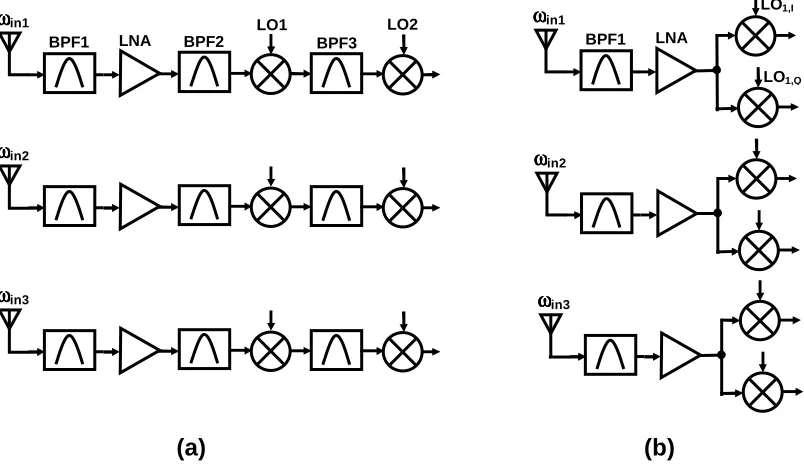
Probably the most trivial solution for a concurrent multi-band receiver is to have a number of single-band receivers in parallel and use each for one particular frequency band. Figure 3.1 shows examples of the aforementioned implementation where each single-band receiver is using a standard heterodyne architecture in (a), and direct down-conversion architecture in (b). More generally, different architectures for each of the parallel receivers can be conceived.
Figure 3.1: Concurrent receiver implementations using multiple parallel single-band, receivers in (a) heterodyne (b) direct down-conversion architectures
3.2.2
Parallel Receivers with a Wide-Band Front-End
A receiver with a wide-band front-end consisting of an antenna and low-noise amplifier (LNA) that can collect signal power at a large range of frequencies followed by appropriate down-converters can be used to receive any number of frequency bands within that range. In Figure 3.2, a broadband front-end is followed by separate down-conversion paths for each frequency band. This scheme might have some advantage in terms of chip area and/or power consumption over the previous method, depending on the implementations of wide-band LNA6. The direct down-conversion architecture of Figure 3.2 (b) is fairly versatile in that by controlling the local oscillator frequency, the operation bands of the concurrent receiver can be varied.
Broadband front-end nevertheless suffers from a serious shortcoming: it not only receives the frequency bands of interest, but also all the other undesirable frequencies get amplified by it. These unwanted signals might have a large signal power and can potentially
6
It is also noteworthy that normally antenna size increases with its bandwidth.
LO1 LO2
LNA BPF2 BPF3
BPF1
ω ω ω ωin1
ω ω ω ωin2
LO1,I
LNA BPF1
ω ω ω ωin1
LO1,Q
ω ω ω ωin2
ω ω ω ωin3
(a) (b)
limit the dynamic range of the receiver due to the nonlinearities inherent to any implementation.
Figure 3.2: Concurrent receiver implementation using a wide-band front-end in (a) heterodyne (b) direct down-conversion architectures
3.2.3
Parallel Receivers with a Multi-Band Front-End
The shortcoming of the previous architecture can be improved by replacing the wide-band front-end with one that has a multiple narrow-band response at frequency bands of interest (Figure 3.3). This multi-band front-end consists of a multi-band antenna (e.g., [28]-[30]), followed by a multi-band filter (e.g., [31]) and a concurrent multi-band LNA that provides simultaneous gain and matching with a low added noise at multiple frequency bands [26]. More discussions on the design of a concurrent multi-band front-end will be provided in section 3.3.
LO1 LO2
broadband LNA
BPF2 BPF1
broadband antenna
(a) (b)
broadband LNA broadband
antenna
LO1,I
Figure 3.3: Concurrent receiver implementation using a multi-band front-end in (a) heterodyne (b) direct down-conversion architectures
3.2.4
Multi-Band Sub-Sampling Receiver
According to Shannon’s original statement of sampling theorem, any signal that contains no frequencies higher than BW [Hz] can be completely determined by discrete samples of the signal spaced (1/2 BW) [sec] apart [21]. Sampling of band-limited signals has been extended to bandpass signals that have energy in the frequency interval (fL, fU) where
BW=fU-fL [22]. The classical bandpass theorem for uniform sampling states that the signal
can be reconstructed if the sampling rate is at least fs(min)=2fU/n, where n is the largest
integer within fU/BW. A graphical representation of bandpass sampling in the frequency domain can be seen in Figure 3.4. In the frequency domain, the effect of uniform sampling is equal to repeatedly shifting the signal by integer multiples of the sampling rate, fs. If these shifted versions of the signal can not be superimposed on one another, the original signal can be recovered easily with appropriate filtering. Using this graphical representation, the aforementioned condition for permissible sampling rates can be derived. There are two important observations in the bandpass sampling scheme. First, note that the sampling rate can be much lower than the center frequency of the signal. Second, we not only can recover the signal in its original form by filtering at the correct center frequency,
LO1 LO2
multiband LNA
BPF2 BPF1
multiband antenna
(a) (b)
LO1,I
LO1,I
multiband LNA multiband
antenna
but also can filter any other replica of the signal and effectively shift the center frequency of the signal without disturbing its frequency contents. This point has instigated schemes that use the so-called sub-sampling to down-convert the RF signal to a lower frequency [23],[24]. Subsampling receivers traditionally have a good linearity performance, but have the disadvantage of noise-folding and hence a lower SNR at the output. As shown in Figure 3.4, both the signal and the wide-band background noise are shifted several times, the latter resulting in an increased total in-band background noise. Filtering the bandpass signal prior to sampling can lower the noise and increase the receiver sensitivity.
Figure 3.4: Frequency domain representation of down-conversion using bandpass subsampling
Bandpass subsampling can be further expanded to bandpass signals. Similar to the previous case, expressions for permissible sampling rates can be derived (e.g., [25]). Once again, Figure 3.5 shows the essence of this concept without any mathematical details and can be used to find the allowable rates for any set of discrete signals. In practice, the frequency bands of interest might not have the same bandwidth and most likely are not equally spaced
sampling rate
noise floor
f
f
BW
fu
fL
fs
increased noise floor Ts=1/fs
Ts
sampler low-pass
filter
in frequency domain. This may result in very low sampling rates which will consequently increase in-band noise due to noise-folding. Therefore, a multi-band filtering scheme is desired at the front-end to limit the effect of out-of-band noise. Additionally, using the multi-band filtering instead of a wide-band front-end is required to reduce the undesirable interferences that limit the dynamic range of the receiver as previously discussed.
Figure 3.5: Frequency domain representation of multi-band subsampling
3.2.5
Direct Digitization (Digital Radio)
Most modern wireless radio receivers down-convert the input RF signal to a lower frequency (intermediate frequency, IF, or baseband) and then convert the low-frequency analog signal to a digital one for further processing. With the rapid improvement in device technology providing faster, smaller, and cheaper active elements, digital circuits are now capable of operating at GHz range frequencies. Hence, there is a large interest in moving the analog-to-digital conversion to higher frequencies (Figure 3.6). Versatile digital circuitry can then process the high-frequency signal (e.g., filter, demodulate). Ideally, such a digital processor can be programmed to process signals at different frequency bands and standards (software defined radio), as well as multi-band signal structures. In theory, direct digitization of a radio-frequency signal is an intriguing idea, but there are extremely difficult challenges in practice with the current technologies. High resolution
analog-to-sampling rate
f
f fs

![Figure 2.4: A direct-conversion multi-band receiver for mobile-phone applications [15]](https://thumb-us.123doks.com/thumbv2/123dok_us/8926921.964918/36.612.130.532.88.289/figure-direct-conversion-multi-receiver-mobile-phone-applications.webp)
![Figure 2.5: Dual-band receiver based on Weaver’s image-rejection scheme [9]](https://thumb-us.123doks.com/thumbv2/123dok_us/8926921.964918/37.612.137.520.83.348/figure-dual-receiver-based-weaver-image-rejection-scheme.webp)