http://dx.doi.org/10.4236/opj.2016.65012
An Improved Design for an All-Optical
Flip-Flop Based on a Nonlinear 3-Sections
DFB Laser Cavity
Hossam Zoweil
City of Scientific Research and Technology Applications, Advanced Technology and New Materials Research Institute, Alexandria, Egypt
Received 11 March 2016; accepted 27 May 2016; published 30 May 2016
Copyright © 2016 by author and Scientific Research Publishing Inc.
This work is licensed under the Creative Commons Attribution International License (CC BY). http://creativecommons.org/licenses/by/4.0/
Abstract
A new all optical flip-flop based on a 3-sections nonlinear semiconductor DFB laser structure is proposed and simulated. The operation of the device does not require a holding beam. Electrical current injection into an active layer provides optical gain to the laser mode. The wave-guiding layer consists of a linear grating section centered between 2 detuned nonlinear grating sections. The average refractive index in the nonlinear sections is slightly higher than the refractive index of the middle section. A negative nonlinear refractive index coefficient exists along the nonlinear sections. In the “OFF” state, the DFB structure does not provide enough optical feedback to lase due to the detuned sections. At high light intensity in structure, “ON” state, detuning decreases and the DFB structure allows for a laser mode that sustains the decrease in detuning to exist. The non-linearity is provided by direct photon absorption at the Urbach tail. Numerical simulations using GPGPU computing show nanoseconds transition times between “OFF” and “ON” states.
Keywords
All-Optical Flip-Flop, Distributed Feedback Laser, Nonlinearity, Switching
1. Introduction
optical flip-flop are suggested and implemented. In [2], an all optical flip-flop based on a micro disk laser where the two states correspond to clock-wise and anti-clock-wise mode is implemented. An all optical flip-flop based on coupled micro laser rings is implemented in [3]. Flip-flop based on a single DFB laser structure is shown in [4]. All optical flip-flops based on multi-mode interference bistable laser diode are described in [5]-[7]. All these flip-flops require a holding beam, or, some of them gererate output modes in both ON and OFF states. All opti-cal flip-flops based on bistable laser diode are discussed in [8] [9], and they do not require a holding beam. In [8] [9], the flip-flop is Fabry-Perot laser cavity that includes a saturable absorber, where the optical loss in the cavi-ty is reduced at high light intensicavi-ty in the laser cavicavi-ty. In [10], an all optical flip-flop based on a DFB structutre with a periodic negative nonlinearity is simulated. The flip-flop does not require a holding beam, and it requires a periodic negative nonlinear coefficient that alters the grating strength which is difficult to fabricate. In [11], an all optical flip-flop based on a chirped nonlinear DFB structure is simulated. In this structure, the chirped grating prevents lasing due to the lacking of an optical feedback (OFF state). The negative nonlinear coefficient in-creases in magnitude linearly along the structure. The chirp is reduced when high optical power exists in the structure (because the nrgative nonlinear coefficient reduces the revractive index along the structure gradually) and a laser mode builds up. The structure in [11] requires a gradual increase in the linear refractive index of the wave guiding layer which is difficult to achieve. Also, it requires a gradual increase in magnitude of the nonli-near coefficient along the wave-guiding layer. This design could be achieved by using multiple sections of dif-ferent linear and nonlinear coefficients. Each section has constant linear refractive index and constant negative nonlinear coefficient. However each section has slightly different linear and nonlinear coefficient as both of them must increase gradually along the structure. This could be difficult to fabricate, and we look for another simpler design.
In this work, an improved design is introduced. The device design is symmetric and requires less injected current. A novel all-optical flip-flop based on a 3-sections nonlinear DFB laser structure is proposed. The device allows for a bistable operation as is [11], but with a simpler structure. In the following sections the device opera-tion is discussed, a mathematical model is introduced and solved numerically using Rung-Kutta method.
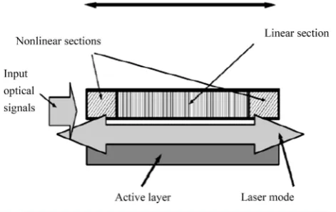
2. Device Configuration and Operation
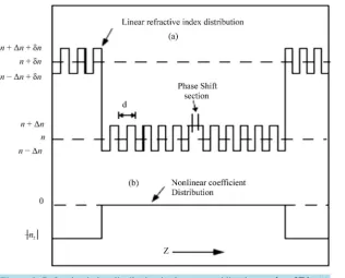
The device schematic is shown inFigure 1. It consists of a nonlinear 3-sections waveguide, and the optical gain is provided by electrical current injection to an active layer. The middle section is a phase-shifted grating. The distribution of refractive index grating and negative nonlinear coefficient is shown inFigure 2, λ =G 2nd is
[image:2.595.197.433.560.709.2]the wavelength at the center of the reflection band of the grating, and d is the grating period. At low light inten-sity in the structure, the grating structure does not provide enough optical feedback to start a laser mode due to the detuning of the nonlinear sections (δn) from the linear grating at the middle of the wave-guiding layer. When an input optical pulse is injected to the device, the detuning of the two nonlinear sections is reduced due to the negative nonlinear coefficient −n2 as in Figure 2. The flip-flop design investigated in this work has advantages over the the design described in [11]. First, while the structure in [11] has a gradual increase in the refrative index and the nonlinear coefficient along the waveguide, the structure introduced in this work has only
Figure 2. Refractive index distribution in the wave-guiding layer, λG=2nd; (a) linear, (b) non-linear.
two nonlinear sections of constant refractive index. Hence the structure shown in this article is easier in fabica-tion. Second, the structure shown in [11] is not symmetric; in the ON state the output laser powers from both ends are not equal in steady state, however the structure studied in this article is symmetric. In steady state (in the ON state) the output optical power from both ends, of the suggested device, are equal. Also, the device in-vestigated in [11] requires a high a injected current because in the OFF state the feedback grating is a chirped grating, and it requires high optical power and high injected current to reduce the chirp and to achieve lasing in the ON state. However in this work, in the OFF state, the feedback grating are not shirped but detuned, and the feedback grating sections require less injected current to achieve the lasing in the ON state.
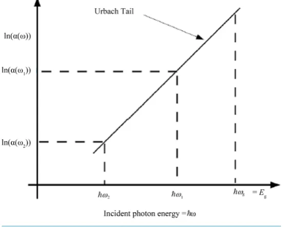
Schematic of the device is shown in Figure 1. The refractive index distribution along the non-linear wave-guiding layer is shown inFigure 2. Electrical current injected to the active layer provides the optical gain. The device requires large negative nonlinear coefficient in the nonlinear grating sections. The negative nonlinear coefficient at the two nonlinear sections is provided by direct photon absorption at the Urbach tail, Figure 3. Part of the photons propagating in the device is absorbed and generates electron-hole pairs. The electron-hole pairs generated reduce the refractive index at incident photon energies slightly less than the semiconductor band gap energy [12]. At low light intensity in the device, due to detuning of the two nonlinear sections from the cen-ter linear grating part, the DFB structure does not provide enough optical feedback to initiate a laser mode. To switch the device “ON”, an optical “Set” pulse of photon energy slightly less than the band-gap energy of the nonlinear section of the waveguide (photon energy ω=ω1,Figure 3) is injected into the device. Part of the injected photons is absorbed (by direct absorption) and generate electron-hole pairs that reduce the average re-fractive index (and the detuning) of the nonlinear sections. Hence, both nonlinear sections contribute to the opt-ical feedback along the structure. As the optopt-ical feedback increases, the DFB structure allows for an optopt-ical laser mode to exist. The optical laser mode intensity maintains the reduction in refractive index in the nonlinear sec-tions, and the laser mode persists. The device is switched the OFF by cross gain modulation (XGM). An optical “Reset” pulse at lower frequency (ω=ω2, ω2<ω1 Figure 3) is injected to the device. The pulse reduces the optical gain at ω ω= 1, and the laser mode decays. The electron-hole pairs generated by the optical pulse at
2
[image:3.595.162.479.82.337.2]Figure 3. Direct absorption loss at Urbach tail; ln
(
α ω( )
)
versus ω.this case, is reduced and the optical laser mode is not allowed to build up. In this work, ω1 and ω2 were cho-sen such as, λ =1 1500 nm, and λ =2 1560 nm. The device could be built using In GaAsPalloy. The band gap energy of the nonlinear wave-guiding layer could be adjusted by varying the ratios of the constituents of the al-loy, [13], so that the operating photon energy (ω1,Figure 3) lies close to the band-gap energy of the nonlinear section. The design of this device is simpler than the device investigated in [11]. Only two sections in this device require tailoring the band-gap energy of the nonlinear waveguide, but in [11] the band gap energy should be tai-lored along the device. In the following section, a mathematical model that describes optical fields in the device and switching dynamics is presented. Simulation parameters are tabulated and discussed too.
3. Mathematical Model and Simulation Parameters
The laser mode in the device is modeled as 2 counter propagating modes. Coupled mode equations are used to model laser mode in the device [11] [14]. The electric field in the device is presented as:
( )
,( )
, exp[
]
( )
, exp[
]
. .E z t =E+ z t i z i t
β
−ω
+E− z t −i z i tβ
−ω
+c c . The output optical field and the “Set” input pulse both are modeled at ω ω= 1. The “Reset” field is modeled at ω ω= 2, and it is described as a forward propagating wave. The “Reset” pulse frequency is far detuned from the grating central reflection band frequency and no reflection occurs at ω ω= 2. The “Reset” propagating mode is presented by:( )
, Reset Reset( )
, exp[
]
.E z t =E z t i z i t
β
−ω
+c c, and ω ω= 2.(
)
(
( )
)
1 1 2exp 2
2 2
cav
E n E g
i i E i i z i z E
z c t
α
γ φ δβ
+ +
+ −
∂ + ∂ = Γ + + − + Γ +
∂ ∂ (1)
(
)
(
( )
)
1 1 2exp 2
2 2
cav
E n E g
i i E i i z i z E
z c t
α
γ φ δβ
− −
− +
∂ − ∂ = − Γ + + − − Γ − −
∂ ∂ (2)
(
)
1 1
2 2
Reset Reset cav
Reset
E n E g
i i E
z c t
α γ
∂ + ∂ = Γ + + −
∂ ∂ (3)
( )
(
)
(
)
1
,
2π d
1
d c 4
G
z n
n z N i i
N
α ω
δ ξ
λ
Γ = − − +
(4)
2
4
G n
λ
( )
, 2 3(
, 1)
1(
, 2)
2c c
c c
c
N z t N z I z I
BN CN
t
α ω α ω
τ ω
∂ +
= − − − +
∂ (6)
( )
2 3( )
( )
1 1 2 2
,
g current g
g g g g
g
N z t I N
BN CN v g S v g S
t qV τ ω ω
∂
= − − − − Θ − Θ
∂ (7)
( ) ( )
1,2(
)
1,2
1
g tr
g N N
g S ω ω ε − = + (8)
Equations (1) and (2) represent the coupled mode equations of the laser mode and the “Set” pulse. Equation (3) presents the “Reset” pulse. Equations (4) and (5) describe detuning, loss and coupling coefficients (Γ2 is the first harmonic expansion of the refractive index periodic variations). Equation (6) is the rate equation of the generated electron-hole pair density “Nc
( )
z t, ” in the nonlinear waveguide sections. Equation (7) presents therate equation of the electron-hole pairs density “Ng
( )
z t, ” generated in the active layer. Equation (8) shows thedependence of optical gain “g” on frequency.
c is the velocity of light in vacuum, and n is the average refractive index.
α
cav 25 cm 1−
= is the intrinsic loss in the laser cavity. λ =G 2nd is the wavelength at the center of the reflection band of the grating. d is the
grating period. δβ β β= − G, β =2πn λ and βG =2πn λG .
(
z,)
α
ω
is the direct absorption loss at the Urbach tail. The loss at the Urbach tail is expressed as(
)
(
)
0exp E EG E0
α α= − , [15] [16], where E is the incident photon energy in electron-volt (eV), EG is the band gap energy in eV, E0 =0.01 eV, and α0 is the absorption coefficient at E=EG. The loss coefficient in the simulation is chosen as:
α
(
z,ω
1)
=480 cm−1 for 0< <z L 4 and 3 4L< <z L and 0 other wise, and it is the direct absorption coefficient of the laser mode and the “Set” pulse.α
(
z,ω
2)
=19.2 cm−1 for 0< <z L 4and 3 4L< <z L and 0 otherwise, and it is the direct absorption coefficient at the “Reset” pulse frequency ω2. 0.006
n
δ = for 0< <z L 4 and 3 4L< <z L, and 0 otherwise. ∆ =n 0.001. d dn N is the differential change in the refractive index due to the change in the electron-hole pairs density generated in the semiconduc-tor at few tenth of electron volts below the conduction band edge. in the simulations −d dn N = −10−26m3, [17].
ξ
=0.033; it is the ratio between change in the refractive index due to the electron-hole pairs and the opt-ical loss generated by the electron-hole pairs density.current
I is the current injected to the active layer. q is the electron charge. V is the active laser cavity volume.
1
I is the power intensity of the optical field at ω ω= 1. I2 is the power intensity of the optical field at
2
ω ω= . g
( )
ω
is the differential optical gain and it depends of frequency (wavelength). In the simulations,( )
2 0.2( )
1g
ω
= ×gω
. S1, and S2 are the photons densities in the cavity at ω ω= 1 and at ω ω= 2 respec-tively, and S=S1+S2.φ
( )
z in equations (1) and (2) counts for the phase shift at the middle of the grating. Its value is:φ
( )
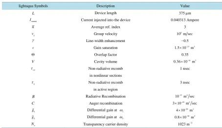
z =π for L 2< <z L and 0 otherwise. It was assumed that no reflections occur at both ends of the DFB structure. Other simulation parameters are shown inTable 1, Refs. [11] [14].It was assumed, in the simulations, λG =λ1=1500 nm. Spontaneous emission fields are added after each
in-tegration step to the forward propagating field and to the backward propagating field.
The system of differential equations is solved using Rung-Kutta technique. The length of the device is divided into 80 sections.
General purpose graphics processing unit (GPGPU) computing is used to perform long simulation time (150 nanosecond). This is done by distributing the computation load along the length of the device among 80 parallel threads that compute the forward and backward fields in the next time step simultaneously. The parallel compu-tation decreases the compucompu-tation time. The numerical simulations use a PC (processor: intel Core i3-4130 CPU at 3.40 GHz × 4, and 32 GB RAM) and graphics processing unit (GPU) Nvidia GeForce GTX 670. The program is coded using Cuda C, [18].
In the following sections, optical bi-stability and ON/OFF switching dynamics in time domain are investi-gated by solving the mathematical model numerically.
4. Numerical Simulations and Discussion
In the following simulations, the output optical laser power is I=2
(
E+2+ E−2)
η
, η is the impedance ofTable 1. Simulation parameters.
lightaqua Symbols Description Value
L Device length 375 µm
current
I Current injected into the device 0.040313 Ampere
n Average ref. index 3
g
v Group velocity 8
10 m sec
γ Line-width enhancement −0.5
Gain saturation 23 3
1.5 10× − m
Θ Overlap factor 0.35
V Cavity volume 16 3
0.36 10× − m
car
τ Non-radiative recomb 1 nsec
in nonlinear sections
g
τ Non-radiative recomb 3 nsec
in active region
B Radiative Recombination 23 6
10− m sec
C Auger recombination 40 6
3 10× − m sec
1
g Differential gain at ω1
20 2
4 10× − m
2
g Differential gain at ω2
20 2
0.8 10× − m
tr
N Transparency carrier density 1023 m−3
the Electric fields are normalised to E0, that is in the field equations E+ −, are replaced by E+ −, E0. Also the
integration steps; ∆z is replaced with ∆z L
(
80)
, and ∆t is replaced with c t nL∆( )
. The electron-hole pairs density in the nonlinear wave-guiding section Nc is normalized to N0=1023m−3. The electron-hole pairs density injected into the active layer Ng is normalized to Ntr. The other coefficients are compensated according to these normalizations.4.1. Current versus Optical Laser Mode Power Bi-Stability
Optical output mode power versus electrical current injected bi-stability is calculated as follow. The injected current to the device is increased from 0 to 0.08 Ampere in 75 nanosecond linearly. Then, the current is de-creased linearly till it reaches 0 in an another 75 nanosecond. Optical bi-stability loop is shown inFigure 4. To insure bi-stable operation of the device, the injected current Icurrent is chosen to be 0.040313 Ampere in all the following simulations. Despite the high optical loss (480 cm−1) due to direct absorption) at 0< <z L 4 and
3L 4< <z L the device produces laser output mode over a range of injected current. This is due to that the central part of the device (L 4< <z 3L 4) behaves as the resonance cavity of the device with a low optical in-trinsic loss (25 cm−1). This central part, at low light intensity in the device, does not provide enough optical feedback to produce a laser mode. This is due to the high escaping rate of photons at z=L 4 and at z=3L 4. At high light intensity in the device, the detuning is decreased in both nonlinear sections, the gratings in these sections start to reflect back photons produced in the central part (L 4< <z 3L 4) and the escaping rate of photons at z=L 4 and at z=3L 4 is reduced. Hence the optical gain in the central part surpasses the optical loss and a laser mode builds up. The role of the two nonlinear grating sections is to produce extra reflections to the escaping photons, and hence the two sections increase the optical feedback along the structure at a high light intensity output. The optical loss (due to direct absorption) at the two sections reduce the output optical power but the optical gain boosts the output optical mode power. The output power level difference between ON and OFF states is 10 log
[
PON POFF]
160 dB.4.2. OFF and ON States
Figure 4. Bi-stability loop; current versus output optical power at z=L.
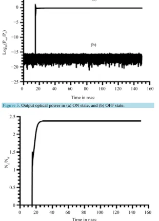
The device is switched ON by a Set pulse at λ λ= 1=1500 nm of 5 10× −6 Watt and 0.37 nsec width (1.87 10× −3picoJoule). The optical pulse is sent through the device (at z=0) at simulation time of 15 nsec. The output optical power level in shown inFigure 5 (Upper curve (a)).Figure 5 (Lower curve (b)) shows the output in the OFF state.
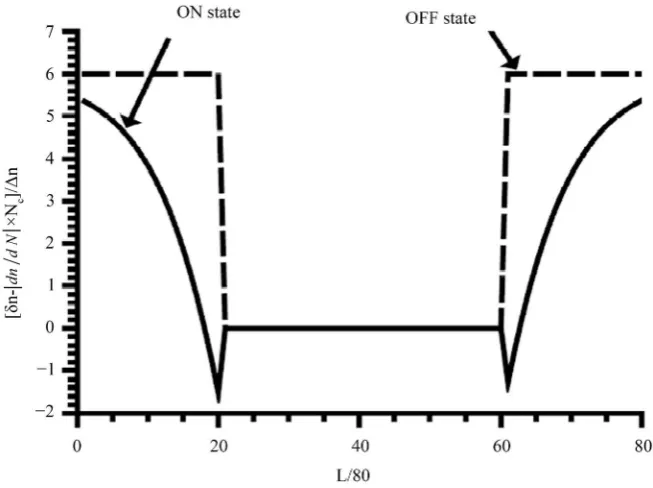
A part of the input pulse energy (photons) is absorbed in the nonlinear wave-guiding sections. It generates electron-hole pairs that reduce the refractive index in each nonlinear section. This decrease in refractive index decreases the detuning in these sections. Hence, the reflection band of each nonlinear section starts to overlap with the reflection band of the middle phase-shifted grating. The optical feedback (reflections) from both nonli-near sections increases, an optical laser mode builds up in the central part of the nonlinonli-near grating section. The optical power of the laser mode maintains the changes in the refractive index in both nonlinear sections.Figure 6 shows the evolution of electron-hole pairs density Nc with time at z=7L 8.Figure 7 shows the evolution of Ng with time at z=7L 8 . The distribution of the refractive index in both nonlinear sections
d d c
n n N N n
δ
− ∆
(Normalized to ∆n) along the device is shown in Figure 8. The broken line and the solid line present the refractive index distribution in the OFF state, and in the ON state respectively. In the OFF state, very low optical power exists in the structure (Optical fields are due to spontanous emission). Nc-the electron-hole carriers density produced by spontanous emissions-is neglegible. Hence
d d c 0.006
n n N N n
δ
− ∆ =
(the brocken line inFigure 8). When the device is switched ON, Nc increases and the detuning at the vicinity of z=L 20 and z=L 60 is reduced where optical fields are reflected back to the grating section L 20< <z L 60.
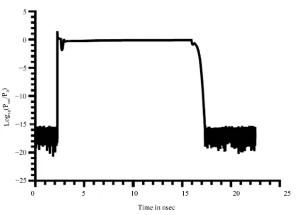
4.3. Set-Reset Operation
Set-Reset operation is simulated in time domain for 22.5 nsec. At t = 22.5 nsec from the start of simulation time, an input optical pulse (Set pulse) at λ λ= 1=1500 nm of 5 10× −6 Watt (20P0 peak power), 0.375 nsec width (1.87 10× −3picoJoule) switches the device ON,Figure 9. Another optical pulse (Reset pulse at
2 1560 nm
λ λ= = ), at t = 15.93 nsec of 2.5 10× −6 Watt (10P0 peak power) and 2.81 nsec width switches the device OFF,Figure 9. The Reset pulse energy is 7.03 10× −3picoJoule.
The output optical power is shown inFigure 10. The Reset pulse reduces the optical gain at λ λ= 1 by XGM,
Figure 5. Output optical power in (a) ON state, and (b) OFF state.
Figure 6. ON state; Electron-hole pairs density at z=7L8 in the nonlinear section.
4.4. Multiple Set-Reset Operations
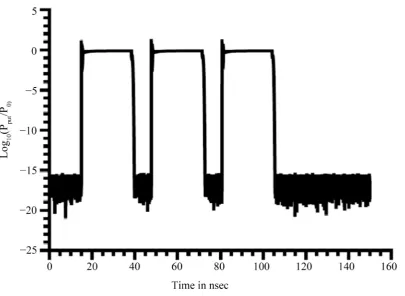
Multiple Set/Reset operations are simulated for 150 nsec.
The input pulses are shown inFigure 13. Input pulses (at λ λ= 1) of power 20P0, 0.37 nsec width, at simu-lation time t = 15 nsec, 47.81 nsec, and 80.62 nsec set the device ON. The Reset pulses (at λ λ= 2) of 10P0
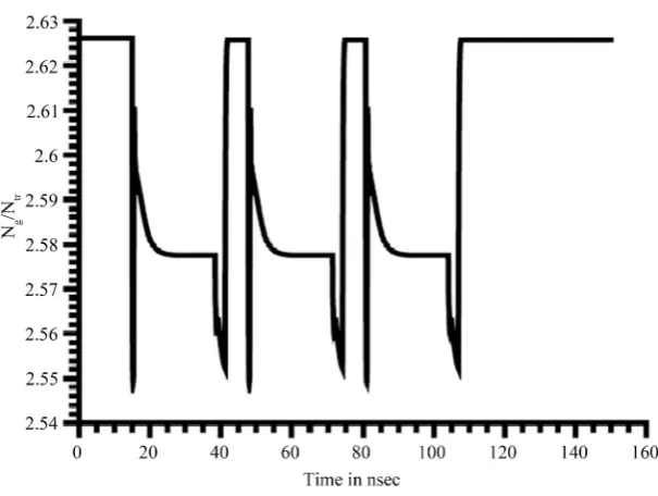
power and 2.81 nsec width are sent at simulation time t = 38.43 nsec, 71.25 nsec, and 104.06 nsec to switch the device OFF. The output optical power is shown in Figure 14. Nc evolution with time during operations at
7 8
[image:8.595.161.472.106.537.2]z= L is plotted inFigure 15. Electron-hole pairs density in the active layer Ng at z=7L 8 is shown in
Figure 16.Figure 14 shows stable output optical pulses where the output optical power between a Reset pulse and the next SET pulse is at 10 log
[
POFF PO]
−160 dB. Also, the output optical power is stable at at POFF [image:8.595.170.459.326.545.2]Figure 7. ON state; Electron-hole pairs density in the active layer at z=7L8.
Figure 8. Distribution of refractive index change in ON state, and OFF state.
in the time interval between the RESET pulse and the next SET pulse, and after the multiple operations elapse. This is the same value in the OFF state. During the RESET operations Nc N0 decays fast compared to the RESET operations described in [11]. Hence, the design presented in this work improves the flip-flop operation speed.
5. Conclusion
[image:9.595.150.477.324.568.2]Figure 9. Set pulse (first pulse), and reset pulse (second pulse).
[image:10.595.108.526.405.708.2]Figure 11. Ng Ntr in the active layer during Set/Reset operation at z=7L8.
[image:11.595.111.519.400.704.2]Figure 13. Input pulses for multiple Set/Reset operations.
[image:12.595.116.522.411.707.2]Figure 15. Nc N0 evolution with time at z=7L8 for multiple Set/Reset
op-erations.
Figure 16. Ng Ntr evolution with time at z=7L8 for multiple Set/Reset op-erations.
is used to solve the mathematical model using parallel computing to be able to decrease the integration step and to be able to reduce the simulation time. The switching dynamics are investigated and show switching between different states in nanosecond time scale. The device is switched ON with a 1.87 10× −3picoJoule pulse of width 0.37 nsec at
λ
=1500 nm. A 7.03 10× −3picoJoule and 2.81 nsec width optical pulse atλ
=1560 nmswitches the device OFF. The device could be used as an all-optical memory element for applications such as all optical processing and routing of optical data packets.
References
[image:13.595.162.465.336.564.2]Optical Packet Switching and Buffering by Using All-Optical Signal Processing Methods. Journal of Lightwave Tech-nology, 21, 2-12. http://dx.doi.org/10.1109/JLT.2002.803062
[2] Liu, L., Kumar, R., Huybrechts, K., Spuesens, T., Roelkens, G., Geluk, E.J., de Vries, T., Regreny, P., Thourhout, D.V., Baets, R. and Morthier, G. (2010) An Ultra-Small, Low-Power, All-Optical Flip-Flop Memory on a Silicon Chip. Na-ture Photonics, 4, 182-187.
[3] Hill, M.Y., Dorren, H.J.S., de Vries, T., Leijtens, X.J.M., den Besten, J.H., Smalbrugge, B., Oei, Y.S., Binsma, H., Khoe, G.D. and Smit, M.K. (2004) A Fast Low-Power Optical Memory Based on Coupled Micro-Ring Lasers. Nature, 432, 206-208. http://dx.doi.org/10.1038/nature03045
[4] Huybrechts, K., Morthier, G. and Baet, R. (2008) Fast All-Optical Flip-Flop Based on a Single Distributed Feedback Laser Diode. Optics Express, 16, 11405-11410. http://dx.doi.org/10.1364/OE.16.011405
[5] Takenaka, M., Raburn, M. and Nakano, Y. (2005) All-Optical Flip-Flop Multimode Interference Bistable Laser Diode.
IEEE Photonics Technology Letters, 17, 968-970. http://dx.doi.org/10.1109/LPT.2005.844322
[6] Jiang, H., Chaen, Y., Hagio, T., Tsuruda, K., Jizodo, M., Matsuo, S., Xu, J., Peucheret, C. and Hamamoto, K. (2011) All-Optical Flip-Flop Operation Based on Asymmetric Active-Multimode Interferometer Bi-Stable Laser Diodes. Op-tics Express, 19, B119-B124. http://dx.doi.org/10.1364/OE.19.00B119
[7] Takeda, K., Takenaka, M., Raburn, M., Kanema, Y., Barton, J.S., Song, X. and Nakano, Y. (2007) Dynamic Operation of All-Optical Flip-Flops with Distributed Bragg Reflectors for Self-Routing of 10-Gb/s Optical Packets. Japanese Journal of Applied Physics, 46, 1028-1032. http://dx.doi.org/10.1143/JJAP.46.1028
[8] Kawaguchi, H. (1997) Bistable Laser Diodes and Their Applications: State of the Art. IEEE Journal of Selected Topics in Quantum Electronics, 3, 1254-1270.
[9] Odagawa, T. (1991) Bistable Semiconductor Laser Diode Device. US Patent No.: 5007061.
[10] Zoweil, H. (2010) Theoretical Modeling of an Improved All-Optical Flip Flop Based on a Nonlinear Semiconductor Distributed Feedback Laser Structure. Applied Optics, 49, 5199-5204. http://dx.doi.org/10.1364/AO.49.005199
[11] Zoweil, H. (2015) Numerical Simulation of a Novel All-Optical Flip-Flop Based on a Chirped Nonlinear Distributed Feedback Semiconductor Laser Structure Using GPGPU Computing. Journal of Modern Optics, 62, 738-744.
http://dx.doi.org/10.1080/09500340.2015.1005186
[12] Bennett, B.R., Soref, R.A. and Del Alamo, J.A. (1990) Carrier-Induced Change in Refractive Index of InP, GaAs, and InGaAsP. IEEE Journal of Quantum Electronics, 26, 113-122. http://dx.doi.org/10.1109/3.44924
[13] Adachi, S. (1992) Physical Properties of IIIV Semiconductor Compounds. John Wiley, Chichester.
[14] Carrol, J., Whiteaway, J. and Plumb, D. (1998) Distributed Feedback Semiconductor Laser. IEE, London.
http://dx.doi.org/10.1049/PBCS010E
[15] Pankove, J.I. (1965) Absorption Edge of Impure Gallium Arsenide. Physical Review, 140, A2059-A2065.
http://dx.doi.org/10.1103/PhysRev.140.A2059
[16] Dow, J.D. and Redfield, D. (1972) Toward a Unified Theory of Urbach’s Rule and Exponential Absorption Edges.
Physical Review B, 5, 594-610.
[17] Haug H., Ed. (1988) Optical Nonlinearities and Instabilities in Semiconductors. Academic Press, Inc., Mitchigan.