Optimization of Delay and Energy in On-Chip Buses
using Bus Encoding Technique
Souvik Singha
Dept of ECENational Institute of Technology Durgapur, W.B, INDIA
G. K. Mahanti
Dept of ECENational Institute of Technology Durgapur, W.B, INDIA
ABSTRACT
In very deep sub-micron (VDSM) fault-tolerant busses, crosstalk noise and logic faults caused due to shrinking wire- size and reduced inter-wire spacing are major factors affecting the performance of on- chip interconnects, such as high power consumption and increased delay. In this paper we propose a bus optimization technique which reduce the energy and power-delay using Hamming Single Error Correcting Code. In this coding scheme we implement Fibonacci representation of optimal (7,4) Hamming Code which is more efficient than Single Error correction (9,4) Hamming Code. Also the proposed scheme eliminates crosstalk classes among the interconnects wires, there by reducing delay and energy consumption. The proposed techniques achieves an efficiency of 11% in energy consumption and a reduction of delay with respect to the existing techniques.
Keywords
Bus Encoding, Crosstalk, Coupling capacitance, Delay, Energy Reduction, Hamming Code, Interconnect.
1.
INTRODUCTION
Crosstalk refers to the interaction between signals that are propagating on various lines in the system. Crosstalk is mainly due to the dense wiring required by compact and high- performance systems. High- density and closely laid interconnects result in electromagnetic coupling between signal lines. The active signal energy is coupled to the quiet line through both mutual capacitance and inductances, resulting in noise voltage- currents. This may lead to inadvertent switching and system malfunctioning. It can effect timing, causing a delay failure, it can increase the power consumption due to glitches, and it can cause functional failure because of the signal deviation. Interconnect cross capacitance noise refers to the charge injected in quiet nets, victims, by switching on neighboring nets, aggressors, through the capacitance between them. This is perceived to be one of the significant sources of noise in current technologies. Cross capacitance can also affect delay and slew depending on whether the aggressor signals are switching in the same or in the opposite direction to the victim net. Amplitude of the signal generated on the passive line is directly related to the edge rate of the signal on the active line, the proximity of the two interconnects and distance that the two interconnects run adjacent to one another. The transition in three neighbors interconnects and their crosstalk, class and delay.
Power consumption and delay are two of the most important constraints in current- day on-chip bus design. The two major sources of dynamic power dissipation on a bus are the self capacitance and the coupling capacitance. As technology scales, the interconnect resistance increases due to shrinking wire-width at the same time increase in the coupling capacitance, leads to stronger crosstalk effects between the interconnects. In Deep Sub-Micron technology the coupling
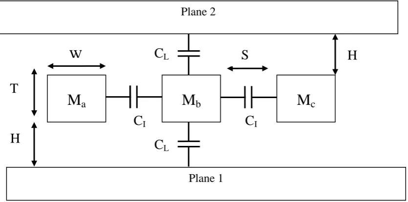
capacitance exceeds the self capacitance which causes more power consumption and delay on the bus [1]. To sum up, with shrinking the feature sizes, increasing die sizes, scaling of supply voltage, increased interconnect density and faster clock rates, the on-chip buses suffer from high power consumption and large propagation delay due to capacitive crosstalk [2, 3]. Since, both power consumed and delay incurred by a system bus increase in the coupling and the self capacitances in modern DSM designs. The problem of reducing capacitive crosstalk effects on buses depends on the transitions on the bus lines. The bus lines are classified as aggressor lines and victim lines depending on the transition activity of the signal they carry. The effect of an aggressor on a victim depends on a number of factors, and not every aggressor will inject an appreciable amount of noise into a victim. In addition, the crosstalk effect may cause a switching wire to inject a noise on an adjacent wire leading to functional defects. The Miller effect suggests that the crosstalk capacitance varies with the switching behavior of a victim wire and its neighbors [4 ]. Besides the increasing sensitivity to noise, also the power dissipation associated with on-chip buses is another relevant issue for VDSM chips. Two major sources of dynamic power dissipation on a bus are the coupling or inter-wire capacitance (CI) and the self or ground capacitance (CL) shown in Fig. 1. The coupling capacitance of an interconnect is the capacitance with respect to the adjacent interconnects running in the same metal plane. Which the self capacitance is the capacitance with respect to metal layers above and below the interconnect. As technology shrinks, the coupling capacitance exceeds the self capacitance causes increased delay and power dissipation on the interconnect lines. Several techniques to reduce the energy consumption by minimizing the transition activity of the bus have been proposed [5, 6]. They are based on a simple capacitive wire model, considering only the bottom capacitance without taking any mutual effect. In fact deep submicron technology has led to a strong reduction of the inter-wire spacing as the wire are relatively higher and closer together. Consequently the wires mutual capacitance has increased as well and has become the main contributor to energy consumption during transition [7]. In this paper we present Fibonacci representation of Single Error Correction (7,4) Hamming Circuits which require less internal nets, cell area and achieve reduced delay and power consumption.
2.
PREVIOUS WORK
based on the inversion of data in data line. This encoding scheme compares the present state of ‘n’ bit line with the previous state of ‘n’ bit data line. Shin et al [11] proposed a similar technique known as partial bus invert coding where the bit lines are consider for inversion in smaller groups instead of the entire bit line. Zhang et al [12] extended BI scheme to propose an improve technique i.e. odd/even bus invert code (OE-BI) which reduces power dissipation by decreasing coupling transitions on the bus. This technique is based on the fact that coupling capacitors are charged and discharged by the active on the neighboring interconnects, where one interconnect bus may have an odd number or even number of interconnects. Jayaprakash et al [13] proposed Partitioned Hybrid Encoding technique where the bus is partitioned optimally and the most efficient energy scheme is applied independently to each partition. Baek et al [14] proposed a low energy set scheme where XOR- XNOR or XNOR- XOR operations are used to transmit data. Subrahmanya et al [15] proposed no adjacent transition (NAT) coding scheme which claims to reduce power consumption and eliminate worst case crosstalk. Lampropoulos et al [16] proposed modified bus invert (MBI) scheme to reduce inductive crosstalk. This scheme inverts the data patterns to minimize transition in the same direction. The bus lines are partitioned into pairs and each pair of adjacent interconnects as well as their previous values are the input of the logic cell. Chen et al [17] developed a mathematical model for a memory less encoding scheme where the encoding and decoding circuits are implemented using simple combination logic. Further more they proposed a novel partitioning method for significant reduction of transition energy dissipation due to coupling capacitance between adjacent wires. Akl et al [18] proposed Transition Skewing Coding (TSC) scheme for reduction power dissipation and area. The total number of repeaters is reduced considerably leading to a reduction in devices area and leakage power. Peak energy and peak current are reduced due to the reduction in simultaneous transitions on the bus. The average power reduction increase as the input switching activity increases. Transition Pattern Coding Scheme (TPC) proposed by Sotiriadis and Chandrakasan [19] is used to reduction of coupling power in the data bus with encoding. This scheme creates transition matrix for selecting code word patterns such that neighboring bus line changes values in the same direction. Thus coupling capacitance and inter-wire energy is reduced. Zhang et al [20] presented a bus encoding method based on code word selection for enduring crosstalk-induced effects, which avoid crosstalk and provide error correcting as well. The methods find a subset from crosstalk avoidance code (CAC) to provide single error correction.
Many encoding methods have been presented to reduce the power dissipation on buses. The bus invert method proposed in achieves a 50% reduction in the maximum number of self transitions and coupling transitions when compared to a normal transmission over an un encoded bus. A bus encoding technique to simultaneously minimize power consumption and eliminate crosstalk delay is proposed in [1]. This technique requires large number of extra interconnects. Another bus encoding technique to minimize both energy and delay is proposed in [1,2,7], which can eliminates only the crosstalk classes 4 and 6. Here the worst case delay is still due to the class 5 transitions, which is high. In [3] a bus encoding is proposed to obtain 10% energy reduction alone with delay reduction of nearly 50%. Bus encoding techniques to reduce the worst case crosstalk delay by nearly 50% are proposed in
[2,5]. However these techniques require large number of extra wires.
3.
ANALYTICAL MODELS FOR DELAY
AND ENERGY CONSUMPTION
Consider a bus with n lines, let dt = ( dt1, dt2, … dtn ) denote the tth n-bit data transmitted on the bus. The delay for transmitting the ( t+1 )th data on the bus is given by the following formula [21,25]. Defining Tk ( dt , dt+1 ), 1 ≤ k ≤ n,
n
k
n
k
k
R
C
d
d
T
n n n k k k T L t t k)
)
1
(
(
1
)
)
(
)
2
1
(
(
1
)
)
1
(
(
)
,
(
1 1 1 1 2 1 1
Where RT is the total resistance, CL is the ground capacitance, CI is the inter-wire capacitance, 1
.
C
C
and
d
d
L i k t k tk
The propagation delay T ( dt, dt+1), for transmitting dt+1 is defined as follows
T ( dt, dt+1 ) = max { Tk ( dt, dt+1 )| 1≤ k ≤n }.
Similarly, the total energy E( dt, dt+1 ) consumed during the transmission of dt+1 is given by [22,25].
n k t t k tt
d
E
d
d
where
d
E
1
1
1
)
(
,
)
Fig 1: Interconnects of Coupling and Self Capacitance.
In DSM era, the coupling capacitance is significant compared to metal-to-ground capacitance. Therefore nearest neighboring lines experience majority to change excited by an aggressor and further neighboring lines contribute minimally to the capacitive coupling. The delay of the line l of an n bit bus where 1 < l < n for certain combination of transitions. Here
indicates to 0-to-1 transition,
indicates a 1-to-0 transition, “–”
indicates no transition on the line and
is the ratio of coupling capacitance to the bulk capacitance. It is seen in Table 1 that the worst case delay can be significantly higher than the delay in the absence of coupling and the opposite switching pattern of the first neighbors to the victim line creates the worst case delay. This is due to the fact when two lines switch in opposite directions, the effective coupling capacitance between them is largest [23]. In an inductive coupling line, coupling excites an induced current that needs to find a return path in order to form a current loop. But due to the presence of the receiver’s gate capacitance, load at the end of wire, there is no dc path for the return current directly back to ground. In this case the orthogonal layer cannot acts as the grounded plane since mutual inductance between two lines is zero for two orthogonal lines. In this case all higher order neighbors are considered as mutual inductance delays slowly with increasing spacing.4.
ERROR DETECTING/CORRECTING
CODES
The Hamming distance of an error detecting/ correcting code gives the maximum number of error bits that can be detected/corrected. The parity code is able to detect a single bit error or an odd number of bits of soft error. The (7,4) Hamming code is able to correct any single bit error and detect any double bit error. The extended Hamming code including an additional over all parity bit in a (7,4) Hamming code is able to distinguish single bit and double bit errors correct and detect. In general n-bit data encoded in an error detecting and correcting code of n + k + 1 bits with a Hamming distance k + 1 is immune to any k-bit error [24].
5.
ENCODING TECHNIQUE BASED ON
(7,4) HAMMING CODE
In this section we consider the Fibonacci series to implement error detection and correction. We present here the positions 2, 4, 6, 7 are assigned to data bits and positions 1, 3, 5 are allocated to parity bits. The code word is computed based on the following relations.
P1 = D2
D3
D4 --- (1) P2 = D1
D3
D4 --- (2) P3 = D1
D2
D4 --- (3) Now the parity check matrix is given by
1 0 1 1 0 1 0
1 1 0 0 1 1 0
0 1 0 1 0 0 1
H
The data bits and parity bits are positioned accordingly using “Equations (1), (2), (3) generating the code word is given below:
[image:3.595.312.547.585.751.2]1 1 0 0 1 1 0
Table 1. Delay in Transitions line
l1
l
l1Relative Delay
− − − 0
↑ ↑ ↑ 1
− ↑ ↑
1
− ↑ −
1
2
M
a
M
b
M
c
Plane 2
Plane 1
T
H
W
S
H
C
LC
L↑ ↑ ↓
1
2
↓ ↑ −
1
3
↓ ↑ ↑
1
4
Now we multiplying the parity check matrix by the code word produces a ‘syndrome’ is given below:
0
0
0
0
1
1
0
0
1
1
1
0
1
1
0
1
0
1
1
0
0
1
1
0
0
1
0
1
0
0
1
If the syndrome is all zeros, the encoded data is error free as with this case. But if the syndrome has a non zero value, the column in the parity check matrix that matches the syndrome is the position where error has occurred. Flipping the encoded bit in this position will result in a valid code word.
6.
OPTIMAL (7,4) HAMMING CODING
SCHEME
In this section, analyze the Total Energy Cost (TEC) of Fibonacci representation of Single error correction Codes on Cross-talk induced bus delay. We define the total energy cost (TEC) of a code space as the sum of the energy consumed in each transition between two different code words. The TEC of each possible (7,4) FRSEC Hamming Code has been evaluated by computing the transition table for all possible transitions between different code words. Since we consider all the code words equally likely that each bit performs the same number of 0 1 and 1 0 transitions for all the code space which consequently have the same TEC [1]. So the power cost for a given symmetric Hamming code space is:
f V C n
n N
Pd tr . BOT dd2
2 ) 1 (
4 2 ) 2 (
Where Ntr is the total number of transition of each code space and n, Vdd , and f are the number of bus wire, voltage supply and frequency respectively. The terms n-2, 2, n-1 are the number of inner wire bottom capacitances, outer wires bottom
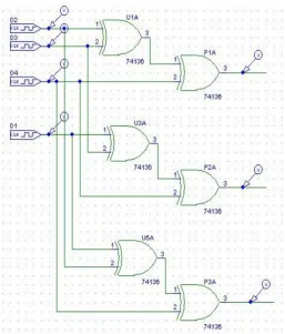
Fig 2: (7,4) Sec Hamming Circuit
capacitances and inter-wire mutual parasitic capacitances, respectively and the values ¼ and ½ take into account that not all transitions require that the capacitances are charged. According to the (7,4) Hamming diagram shown in Fig. 3. The TEC is 2256 CBOT V2dd f. where for the calculation inter wire bottom capacitance is 4, inner wire mutual parasitic capacitance is 2, and outer wire bottom capacitance is 1. The software model of (7,4) Fibonacci representation of single error correction Hamming code shown in Fig. 2.
Where as in case of (9,4) Hamming code [1] (n-2) = 6, (n-1) = 3 and the outer wire bottom capacitance is 2. Hence the TEC is 3452 CBOT V2ddf. considering the
2
.
13
and
7
.
28
. If we consider the same CMOS metal for both the buses CBOT will be same in both cases. For the same voltage supply it is clear from the calculation that the energy is minimized in case of SEC (7,4) Hamming code. The energy reduction is 53% in (7,4) Hamming code compared with (9,4) Hamming code. Hence it optimized. [image:4.595.315.573.69.371.2] [image:4.595.49.287.72.147.2]Fig 3: Optimized Capacitance of a 3 wire bus model using (7,4) Hamming Code.
7.
EXPERIMENTAL RESULTS
.Here we introduced SEC Fibonacci representation of a optimal (7,4) Hamming code which reduced the crosstalk induced bus delay provided by the considered coding techniques and the experimental results shown in Fig. 4. Therefore combining the SEC (9,4) Hamming code with non-uniform inter-wire spacing, that can achieve an energy saving of 12%. It can be noticed that if consider a optimal (7,4) Hamming code with the bus wires at minimum spacing, that can achieve an energy saving of 53% with respect to the (9,4) Hamming code. We also verified the impact of our technique on the power-delay product. This metric is inversely proportional to the power efficiency. We can see that our technique allows a significant improvement in power-delay product compare to the (9,4) Hamming code. In particular the power efficiency proportional to the inverse of the power delay product is 1.8 times better.
8.
CONCLUSION
In this paper we presented a new scheme which allows to reduce the maximum cross-talk induced delay within VDSM buses using Fibonacci representation of Single Error Correcting Code. These results shows that optimal (7,4) Hamming codes have identical energy consumption. The proposed coding scheme allows a energy saving and power delay product reduction of more than 53% with respect to (9,4) Hamming codes.
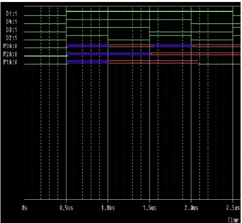
Fig 4: Optimized (7,4) SEC Hamming Circuit Output
Shield
CC CC CC
CE
CE CE
CE
CB CB
Shield
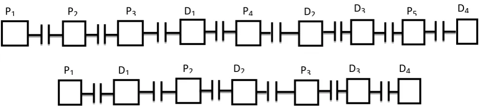
[image:5.595.55.299.508.733.2]Fig 5: Bus Organization of Optimal (7,4) Hamming Code
9.
REFERENCES
[1] D. ROSSI, V.E.S. van Dijk, R.P. Kleihorst, A.H. Nieuwland, C. Metra, “coding Scheme for low energy consumption fault-Tolerant Bus”. Processing of the Eight IEEE International On-Line Testing Workshop (IOLTW’ 02).
[2] C. Duan and S.P. Khatri, 2004. “Exploting crosstalk to speed up on-chip buses”. Processing on the Conference on Design Automation and Test in Europe, pp. 777-783. [3] J. Yim and C. Kung, 1999. “Reducing Cross-coupling
among interconnect wires in deep-submicron data path design”, Processing of the 36th
ACM/IEEE conference on Design Automation, pp. 485-490.
[4] Sachin Sapatnekar, 2004. “Timing”, Kluwer Publisher. [5] S. Ramprasad, N.R. Shambhag, and I.N. Hajj, 1999. “A
Coading Framework for Low-Power Address and Data Busses”, IEEE Trans. On VLSI Systems.
[6] A. Kazeminejad, 2001. “Fast, Minimal Decoding Complexity systematic (13,8) Single-Error-Correcting code for on-chip DRAM Application”, Electronic Letters.
[7] P.P. sotriadis and A. Chandrakasan, 2000. “Bus Energy Minimization by Transition Pattern Coding in Deep Submicron Technologies”. In IEEE/ACM Int. Conference on Computer Aided Design, ICCAD, pp. 322-327.
[8] B. Victor, B. Keutzer, 2001. “Bus encoding to prevent crosstalk delay”, In IEEE/ACM International Conference on Computer Aided Design (ICCAD), pp. 57-63. [9] M.R. Stan, W.P. Burleson, 1997. “Low-power encodings
for global communication in CMOS VLSI”, IEEE Trans on VLSI (TVLSI) 5(4), pp. 444-455.
[10] M.R. Stan, W.P. Burleson, 1995. “Bus-invert coding for low-power I/O. IEEE Trans. On VLSI (TVLSI), pp. 49-58.
[11] Y. shin, S. chae, K. Choi, 2001. “Partial Bus-invert coding for power Optimization of application-specific systems. IEEE Trans. On VLSI 9(2), pp. 377-383. [12] Y. Zhang, J. Lach, K. Skadron, M.R. Stan, 2002.
“Odd/even bus invert with two-phase transfer for buses with coupling”, In: International Symposium on Low Power Electronics and Design (ISLPEd), pp. 80-83. [13] S. Jayaprakash, N.R. mahapatra, 2007. “ Partitioned
hybrid encoding to minimize on-chip energy dissipation of wide microprocessor buses”’ In: 20th
Intl. Conf. on VLSI Design, pp. 127-134.
[14] K.H. Beak, K.W. Kim, S.M. Kang, 2000. “A low energy encoding technique for reducing of coupling effects in SOC interconnects”, In: 43rd
IEEE Midwest Symposium Circuits and Systems, pp. 80-83.
[15] P. Subrahmanya, R. Manimegalai, V. Kamakoti, M. Mutyam, 2004. “A busencoding technique for power and cross-talk minimization”, In: 17th Intl. Conf. on VLSI Design, pp. 443-448.
[16] M. Lampropoulos, B.M. AI-Hashimi, P. Rosinger, 2004. “ Minimization of crosstalk noise, delay and power using a modified bus invert technique:, In: Design, Automation and Test in Europe conference and Exhibition (DATE), vol 2, pp. 1372-1373.
[17] G. Chen, S. Duvall, S. Nooshabadi, 2009. “Analysis and design of memoryless interconnect Encoding scheme”’ In: IEEE International Symp. On Circuits and Systems (ISCAS), pp. 2990-2993.
[18] C.J. Akl, M.A. Bayoumi, 2008. “Transition Skewing Coding for Global On-Chip Interconnects”, IEEE Trans. On VLSI Systems 16(8), pp. 1091-1096.
[19] P.P. sotiriadis, A. Chandrakasan, 2001. “Reducing bus delay in submicron technology using coding”, In: Asia South Pacific Design Automation (ASP-DAC), pp. 1280-1283.
[20] Y. Zhang, L. Huawei, L. Xiaowei, Y. Hu, 2008. “Codeword Selection for Crosstalk Avoidance and Error Correction on Interconnects”, In: 26th
IEEE VLSI Test Symp (IEEE-VTS), pp. 377-382.
[21] P. Sotiriadis and A. Chandrakasan, 2001. “Reducing bus delay in sub-micron technology using coding”, Proceedings of the Asia and South Pacific Design Automation Conference, pp.109-114.
[22] P. Sotiriadis and A. Chandrakasan, 2002. “A bus energy model for deep sub-micron technology”, IEEE transactions on VLSI System, vol. 10(3), pp. 341350. [23] P. Sotiriadis and A. Chandrakasan, 2002. “Low power
bus encoding techniques considering inter-wire capacitances”, Processing of the IEEE International Conference Custom Integrated Circuits, pp. 507-510. [24] T.K. Moon, 2005. ‘Error Correction Coding:
Mathematical Methods and Algorithms”, Wiley-Interscience.
[25] K. Najeeb, Vishal Gupta, V. kamakoti, Madhu Mutyam. “Temporal Redundency Based Encoding Technique for Peak Power and Delay Reduction of On-Chip Buses”, Publications.cse.iitm.ac.in.