FPGA Implementation for Minimum Differential
Feedback of MIMO-OFDM Transreceiver System
Ruchi Sawal
M.Tech SRM University
Chennai, India
B.S.S.Kalyan
M.Tech SRM University
Chennai, India
P.Vijaya Kumar
Asst. professor SRM University Chennai, India
ABSTRACT
The latest Research Trend in wireless communication is implementing wireless system on SDR (Software Define Radio), so the SDR implementation of MIMO-OFDM receiver with channel state information is presented in this paper. Here we use Xilinx 13.1 Spartan 3 xc3s400pq208 FPGA device. The simulation results are obtained for 2x2 MIMO-OFDM receiver system in which we have implemented channel estimation, FFT, deinterleaver and decoder blocks in VHDL. The performance analysis of the receiver implementation is presented with resource utilization and timing analysis.
Keywords
MIMO, OFDM, FPGA, channel estimation.
1.
INTRODUCTION
With the increasing use of wireless communication for data applications such as Internet access and multimedia, the demand for reliable high-data-rate services is increasing rapidly. Wireless channels introduce a variety of impairments in the transmitted signals due to fading, intermittent interference and multi-user interference. The use of MIMO technology can exploit multi-path propagation to mitigate these impairments. MIMO technology uses multiple forms of diversity by using multiple antennas at the transmitter and the receiver. With multiple devices communicating with a single base station at the same time, Multiple Access Interference (MAI) exists in a MIMO multi-user system. In order to combat MAI and to identify the users at the receiver, a suitable MIMO multi-user detection technique is required. Several receiver architectures have been proposed for MIMO multi-user wireless systems. Thus, a MIMO system offers the dual benefits of increased capacity due to spatial multiplexing and fading suppression due to receive/transmit diversity. MIMO systems can increase the data rate and provide multiplexing gain by transmitting different data on different antennas, also known as spatial multiplexing. MIMO systems can also improve the reliability and error performance in the receiver through diversity gain, i.e. providing the receiver with multiple copies of the transmitted signal. MIMO technology draws an attention in wireless communications due to significant increase in data throughput and link range without additional bandwidth or transmitted power. It achieves this by higher spectral efficiency (more bits per second per hertz of bandwidth) and link reliability or diversity (reduced fading) Thus, the present study aims at developing a MIMO transreceiver system based on FPGA based target hardware which offers very high data rate, high noise immunity, reliability and very low bit error rate. The choice of FPGA based design over the traditional VLSI design is also a challenge in this work to achieve an appreciable performance
in much less design cost and design time Field programmable gate arrays (FPGAs) with their inherently parallel structure, are increasingly the technology of choice for addressing the requirements of next generation systems. One of the fundamental areas in many academic and industrial research organizations is in the area of hardware realization of advanced MIMO receivers. In this chapter, we discuss the architectural challenges associated with spatial multiplexing and diversity gain schemes and introduce FPGA architectures and report experimental results for the FPGA realization of these systems. We introduce an architecture and implementation of a spatial multiplexing MIMO detector and its FPGA implementation.
2.
SYSTEM MODEL
The received signals can be given in the form of vector
y = Hx+n (1)
where , x = [ 1, 2, ⋅⋅⋅ , n ] represents a n×1 transmitted
signal vector, and n is a noise vector. y = [ 1, 2, ⋅⋅⋅ , n ]
denotes a n×1 received signal vector, H is a n×n channel fading matrix with independent entries obeying complex Gaussian distribution (0, 2ℎ).
2.1
Channel Estimation
Considering a limited and error-free feedback channel throughCSI quantization
Ĥ= H + E (2)
where H represents the feedback channel output, E represents an independent additive noise matrix and represents the average channel quantization distortion constraint. The quantized CSI can be rewritten as
H= 2ℎ/ 2ℎH+ Φ, (3)
where Φ is independent of Ĥ .
2.2
Differential Encoding
we consider the differential feedback, where only the differential CSI will be sent back to the transmitter, assuming that the previous channel quantization matrix Hn−1 is known
at both the receiver and the transmitter. The differential CSI can be formulated as
H = Diff (Ĥ H−1), (4)
Where H represents the differential CSI between Ĥ and
H−1, and Diff(⋅) denotes the differential function.
2.3
Quantization
H= UΣV (5)
Where U and V represent two unitary matrixes of size n x n and m x m, and Σ is a non-negative and diagonal matrix composed of eigen values of H.
2.4
Differential Feedback
In this section, the minimum differential feedback rate of MIMO block-fading channel is calculated to determine the accuracy of CSI. Minimum differential feedback rate is determined by Rate distortion theory.
3.
HARDWARE MPLEMENTATION
3.1
Design steps of FPGA implementation
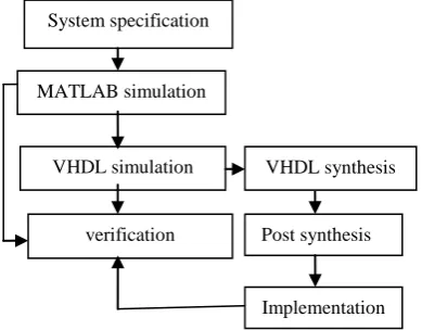
[image:2.595.321.536.282.401.2]MIMO-OFDM implementation process on FPGA is outlined in Fig. 3. The system is first examined with a high level simulation using MATLAB Mathwork .The sub-blocks of the communication system are then translated for hardware implementation. The HDL used in this work is VHDL for its flexibility of coding styles and suitability for handling very large and complex designs.
Fig 1: Design steps of FPGA Implementation
ModelSimSE 6.2c is used to run functional and post place-and route simulations. After compilation, simulation place-and synthesis, configuration files are generated which are further used to be implemented on FPGA device.
3.2
System Description:
The input bit stream is first encoded using punctured convolutional codes with constraint length K=7. The idea of puncturing is to delete some bits in the code bit sequence according to a fixed rule. In general the puncturing of a rate K / N code is defined using N puncturing vectors. Each table contains p bits, where p is the puncturing period. If a bit is 1 then the corresponding code bit is not deleted, if the bit is 0, the corresponding code bit is deleted. The N puncturing vectors are combined in a N x p puncturing matrix P. Next step is interleaving, which is implemented using a block interleaver, whose size varies according to the modulation scheme used and the system configuration. The receiver performs these functions in reverse order to retrieve the data. This is followed by mapping process which is 16-QAM, or
[image:2.595.53.248.331.483.2]64-QAM , which is a method for converting a digital signal to a complex signal. The model modulates the signal onto a sequence of complex numbers that lie on a lattice of points in the complex plane, called the constellation of the signal. A 256-point IFFT forms the OFDM symbol with 192 data, 8 pilots, and 56 null subcarriers forming the frequency guard bands. The IFFT block computes a 256-point IFFT to form an OFDM symbol. A cyclic prefix refers to the prefixing of a symbol with a repetition of the end. Although the receiver is typically configured to discard the cyclic prefix samples Cyclic Prefixes are used in ∑ in order to combat multipath by making channel estimation easy, CP varies between 1/4, 1/8, 1/16, and 1/32 depending on the bandwidth used, which can vary from 1.5 to 28MHz. The completed symbol corresponding to 320 points is then transmitted over the channel.
Fig 2: MIMO-OFDM communication system
4.
SYSTEM IMPLEMENTATION
(MIMOReciever)
4.1
Channel Estimator
To analyze hardware implication of MIMO-OFDM system, receiver section is modeled in VHDL and implemented on FPGA platform. The transmitter section is analyzed through MATLAB simulation.
Input u(n) Output y(n)
u(0),u()1……
- + error e(n)
Fig 3: Block Diagram of Adaptive Algorithm
Channel estimation is the method of estimating the frequency response of the radio channel on which the transmitted signal travels before reaching the receiver. Channel is estimated for every sub-carrier and each spatial path between transmitted and receiver antenna pairs, If the channel is assumed to be linear, the channel estimate is simply the estimate of the impulse response of the system. It must be stressed once more that channel estimation is only a mathematical representation of what is truly happening. A “good” channel estimate is one System specification
MATLAB simulation
verification VHDL simulation
Post synthesis
simulation
Implementation VHDL synthesis
Linear Discrete-time Filter w0,w1,w2……….
[image:2.595.316.521.546.622.2]where some sort of error minimization criteria is satisfied (e.g. MMSE). Channel estimation algorithms allow the receiver to approximate the impulse response of the channel and explain the behavior of the channel.
4.2 Adaptive Algorithm
An adaptive algorithm is an algorithm that changes its behavior based on the resources available. Adaptive algorithms are needed in order to continuously update the filter coefficients. Adaptive filters have been employed in a wide range of fields. However, there are essentially four basic classes of applications for adaptive filters. These are: identification, inverse modeling, prediction, and interference cancellation .
The discrete adaptive filter accepts an input u(n) and produces an output y(n) by a convolution with the filterʹs weights, w(k). A desired reference signal, d(n), is compared to the output to obtain an estimation error e(n). This error signal is used to incrementally adjust the filterʹs weights for the next time instant. Several algorithms exist for the weight adjustment, such as the Least‐Mean‐Square (LMS) and the Recursive Least‐Squares (RLS) algorithms. Least Mean Square LMS algorithm is used in this model for adaptive equalization of the received signal. LMS algorithms is a type of adaptive filter used to obtain a desired filter by finding the filter coefficients to produce the least mean squares of the error signal (difference between the desired and the actual signal). The receiver module is designed to demodulate the faded and distorted signal received from the channel. Here, we have implemented the LMS equalizer and also correlation algorithm is designed to recover the distorted MIMO-OFDM signal. The system is analyzed and was found to give a successful and better result in terms of the Bit Error Rate,[Table-I,II] data rate and efficiency of demodulation and prediction of the receiver.
4.3 Filter Algorithm
Another algorithm used for channel estimation in MIMO receiver system is Filter Algorithm. The VHDL simulation of Filter Algorithm uses two components sum and multiplier. The sum-product algorithm for channel estimation and data detection can be summarized as the following:
1) Step 1: Initialization: Before the first iteration, a raw estimation of the channel is obtained by training symbols. 2) Step 2: Data detection: Use soft information of estimated CFR to determine transmitted bits according to channel observation. Messages containing reliability of the detected symbols are combined to get log likelihood ratios (LLR) of transmitted bits. In case of coded transmission, soft decoding is executed based on LLRs.
3) Step 3: Channel estimation using channel statistics: With the help of successfully detected symbols, soft channel estimation is performed. The soft information is further refined with known channel statistics.
4) Step 4: Step 2 and 3 are repeated until certain stopping criterion is fulfilled. Thereafter, hard decision is made as output.
4.4
FFT
The Fast Fourier Transform (FFT) and Inverse Fast Fourier Transform (IFFT) are derived from the main function, which is called Discrete Fourier Transform (DFT). In DFT, the computation for N-points of the DFT will be calculated one by one for each point.
(6)
(k) represents the DFT frequency output at the k-the spectral point where k ranges from 0 to (N-1). The quantity N represents the number of sample points in the DFT data frame. The quantity x(n) represents the n-th time sample, where n also ranges from 0 to N-1.
4.5 Decimation in Frequency Algorithm
The FFT core uses the radix-4 and radix-2 decomposition for computing the DFT. For two-phase solutions, the time (DIT) method is used, while the decimation-in-frequency (DIF) method is used for the streaming solution. When using radix-4, the N-point FFT consists of log4 (N) stages, with each stage containing N/4 radix-4 butterflies. Point sizes that are not a power of 4need an extra radix-2 stage for combining data. An N-point FFT using radix-2 has log2 (N) stages, with each stage containing.4.6
Interleaver
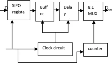
The main purpose of interleaving is to randomize the location of errors introduced in signal transmission. If a particular interleaver is used at the transmit end of a channel, the inverse of that interleaver must be used at the receive end to recover the original data. The inverse interleaver is referred to as a de-interleaver. The type of interleaver/de-interleavers used in our implementation system is Convolutional interleaver.The proposed VHDL model of an 8 bit convolutional interleaver with J = 1 is presented in Fig. 4.
[image:3.595.326.522.449.561.2]Din Dout
Fig 4: Block Diagram of Convolutional interleaver
The Serial Input Parallel Output (SIPO) register first converts the received serial form code word (Din) into an 8 bit parallel code word. The buffer unit then sends a word to the delay unit after every 8 clock cycles. The code word gets scrambled as it progresses through the delay unit. The purpose of scrambling is to reduce the length of strings of 0s or 1s in a transmitted signal, since a long string of 0s or 1s may cause transmission synchronization problems. The scrambled code word is then given to then to the 8 line to 1 line multiplexer (MUX) which converts it into stream of serial data (Dout). The 3 bit counter is used to generate the select input for the MUX. The VHDL model of the deinterleaver is exactly similar to interleaver block In order to verify the VHDL models for deinterleaver from the output of the interleaver is applied as input to the deinterleaver block along with clock as synchronization signal. It is observed that the scrambled code word is converted into its original form at from the output of the interleaver is applied as input to the deinterleaver block.
SIPO registe r
Buff er
Dela y unit
8:1 MUX
4.7. Viterbi Decoder
The functionality of a Viterbi decoder is usually implemented by three functional units: the branch metric unit (BMU); the add-compare select unit (ACSU); and the survivor memory unit (SMU). BMU calculates the distance (metric) between the received noisy symbol and the output symbol of the state transition (branch). ACSU computes the accumulated metric associated with the sequence of transitions (path) to reach a state. When more then a path arrives to a state, ACSU selects the path with the lowest metric value, which is the survivor path. SMU stores the information that permit to trace back from a state to the previous one.
[image:4.595.57.281.208.369.2]IN OUT
Fig 5: Viterbi Decoder Architecture
5.
SIMULATION
RESULTS
AND
ANALYSIS
The whole implementation was hosted in spartan-3 devices (xc3s400pq208) occupying a considerable amount of embedded memories, DSP slices and regular FPGA slices. The Xilinx ISE 13.1 software tool chain was used for the implementation of the FPGA bit streams; the use of this ISE version was mandatory to comply with the VHDL code integration prerequisites of the board manufacturer. Integrating the code of the developed system in the user-logic space of the boards VHDL firmware has revealed numerous engineering challenges.
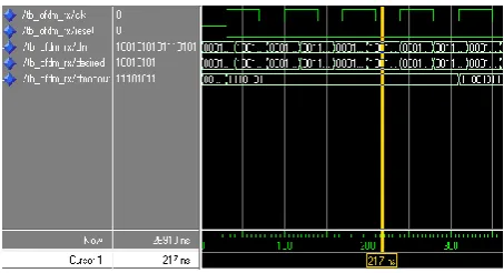
Fig 6: Simulation results of MIMO-OFDM receiver
Fig7: Simulation results of Channel Estimator
[image:4.595.53.280.478.601.2]The above results shows the MIMO-OFDM receiver and channel estimator simulation results using Xilinx13.1 ISE ,with clock set to 0,two inputs one is 16-bit(Din) and 8-bit desired input is given and an 8-bit Dmod output is obtained. The hardware implementation of the design brings out a few important FPGA design issues like resource utilization, timing analysis, time delay which are very important parameters while designing a chip. The following tables shows the design parameter readings which were taken with the help of Xilinx System Generator for Spartan-3 device xc3s400pq208. The speed grade of the device is -5.
Table 1. Resource utilization analysis
GND INV LUT FLIP-FLOPS
CLK BUFFER
1 1 LUT2-36 FD-40 BUFGP-2
LUT3-58 FDC-12 IBUF-41
LUT4-20 FDCE-1 OBUF-40
FDPE-1
Table-2 spartan-3 device utilization analysis
Table-3 Timing Analysis
SECTIONS
Slack =Required time-Arrival time=6.3ns
No of Slices
No of Slice
Flip Flop
No of 4-input LUT
No of bonded IOBs
No of GCLKs
61 out of 2448 -2%
14 out of 4896-0%
115 out of 4896-2%
83 out of 153-52%
2 out of 24-8%
Minimum period
Maximu m frequency
Min i/p Arrival time
Max o/p require d time
Total Delay
3.366ns 297.089M
Hz
4.283ns 10.583n s
3.366n s BMU ACSU01 SMU DU
[image:4.595.55.280.628.712.2]6.
CONCLUSION
In this paper we are presenting an efficient implementation of MIMO-OFDM receiver on an FPGA. We choose an FPGA approach for this system implementation and analysis to obtain an accurate results and to deploy more hardware units. The accuracy in obtained results has been increased with the help of efficient coding in VHDL. The proposed model is highly suitable because of its flexibility, reduced computational complexity and higher throughput.
7.
REFERENCES
[1] J. Ruggiero, T. Bonnema, D. J. Inman, application of SISO and MIMO modal analysis technique.
[2] N. Seifi, A. S. Tehrani, and M. Viberg, ““Simulation of a Wideband Reconfigurable Multi-Antenna System with Space-Time Coding”,” in Nordic Matlab Users Conference, Stockholm, Sweden, Nov. 2008.
[3] G.Foschini and M. Gans, ““On Limits of Wireless Communications in a Fading Environment when Using Multiple Antennas”,” Wireless Personal Communications, vol. 6, pp. 311–335, March 1998. [4] Technique for Wireless Communications”,” IEEE J Sel.
Areas in Comm., vol. 16, no. 8, pp. 1451–1458, Oct. 1998.
[5] H. Huang, “Spatial channel model for multiple input multipleoutput(MIMO)simulations”http://www.3gpp.mo bi/ftp/specs/htmlinfo/25996.htm, Dec. 2004,as read 2008-09-12.2008.
[6] Y. Houand and T. Hase, “New flexible OFDM structure for consumer electronics communication systems,” IEEE Trans. Consumer Electron., vol. 55, no. 1, pp. 191–198, Feb. 2009.
[7] H. Yu, M.-S. Kim, E. young Choi, T. Jeon, and S. Kyu Lee, “Design and prototype development of MIMO-OFDM for next generation wireless LAN,” IEEE Trans. Consumer Electron., vol. 51, no. 4, pp. 1134–1142, Nov. 2005.
[8]J. Soler-Garrido, D. Milford, M. Sandell, and H. Vetter, “Implementation and evaluation of a high-performance MIMO detector for wireless LAN systems,” IEEE Trans. Consumer Electron., vol. 57, no. 4, pp. 1519 –1527, Nov. 2011.
[9] C.-S. Choi, Y. Shoji, and H. Ogawa, “Implementation of an OFDM baseband with adaptive modulations to grouped subcarriers for millimeter-wave wireless indoor networks,” IEEE Trans. Consumer Electron., vol. 57, no. 4, pp. 1541–1549, Nov. 2011.
[10] G. L. Stuber, J. R. Barry, S. W. McLaughlin, Y. G. Li, M. A. Ingram, and T. G. Pratt, “Broadband MIMO-OFDM wireless communications,”Proc. IEEE, vol. 92, no. 2, pp. 271–294, Feb. 2004.
[11] S. M. Alamouti, “A simple transmit diversity technique for wireless communications,” IEEE Journal on Selected Areas in Communications, vol. 16, no. 8, pp. 1451–1458, Oct. 1998.
[12] K.Praveen Bagadi and S. Das, "MIMO-OFDM Channel Estimation Using Pilot Carries," International Journal of Computer Applications, vol. 2, pp. 81-88, May 2010 [13] S.Tiiro, J. Y lioinas, M. MyllyHi, and M. Juntti,
"Implementation of the least squares channel estimation algorithm for MIMO-OFDM systems," ITG Workshop on Smart Antennas, pp. 155-161, Feb. 2009.
[14] S. Haene, D. Perels, and A. Burg "A Real-Time 4-Stream MIMOOFDM Transceiver: System Design, FPGA Implementation, and Characterization," IEEE Journal on Selected Areas in Communications, vo1.26, no.6, pp.877-889, August 2008.
[15] S. Yoshizawa and Y. Miyanaga, "VLSI Implementation of a 4x4 MIMO OFDM transceiver with an 80-MHz channel bandwidth," Circuits and Systems, 2009. ISCAS 2009.
[16] IEEE International Symposium on, vol., no., pp. 1743 1746, 24-27 May 2009. Nirav Shah, "MIMO-OFDM: Theory to implementation,", MS-Thesis, Uinversity of Southern California, 1435118,92 pages, Dec. 2006. [17] Lattice semiconducter sponsored white paper
"Implementation of an OFDM Wireless Transceiverusing IP Cores on an FPGA" ,FPGA and Programmable Logic Journal,Techfocus Media Inc,2005, pages 1-13
[18] Paul A. Lynn, Wolfgang Fuerst,” Introductory Digital Signal Processing with Computer Application, Second Edition”, John Wiley & Sons, England, 1999. 188 [19] Shariat-Yazdi, R.Kwasniewski, T., ”Challenges in the
Design of Next Generation WLAN Terminals”, Canadian Conference on Electrical and Computer Engineering(CCECE), pp. 1483-1486,April.2007. [20] S. Haene, D. Perels, A. Burg, A real-time 4-stream