ISSN Online: 2153-1293 ISSN Print: 2153-1285
A Modified PFD Based PLL with Frequency
Dividers in 0.18-µm CMOS Technology
N. K. Anushkannan
1, H. Mangalam
21Department of Electronics and Communication Engineering, Tamil Nadu College of Engineering, Coimbatore, India 2Department of Electronics and Communication Engineering, Sri Ramakrishna Institute of Technology, Coimbatore, India
Abstract
This paper introduces a modified design of CMOS dynamic Phase Frequency Detec-tor (PFD). The proposed PFD circuit (PPFD) is designed, simulated and the results obtained are analyzed. In order to reduce dead zone, internal signal routing is used in the PPFD circuit. To extend, Phase Locked Loop (PLL) is designed and it is verified with two different Frequency Divider (FD) circuits. There is a decrease in area of the PPFD circuit with 16 transistors and dissipates power of 40.8 pW for 1.2 V power supply. The pre-layout simulation result shows that the PPFD circuit has an elimina-tion of a dead zone. Further, it works with the high speed and reduced power oper-ated in the reference frequency of 50 MHz and the feedback frequency up to 4 GHz.
Keywords
PFD, Dead Zone, VCO, Power, PLL
1. Introduction
A Phase Locked Loop is a closed loop feedback control system which is capable of gen-erating a clock signal that has a fixed relationship to the reference clock signal. It causes a particular system to track with another one [1]. The PLL technique is active around for a long time. It has various applications include keeping power generators in phase, synchronizing to the pulse in a TV set [2], clock recovery from asynchronous data, de-modulating an FM modulated signal and so on. Although there are legitimate applica-tions, the primary use is frequency synthesis. The General block diagram of the PLL is illustrated in Figure 1. The primary function of the PLL is the VCO’s output using ex-ternally present reference signal and output of the frequency divider. Both signals are in phase with each other. Further, the VCO’s output indicates that the phase difference How to cite this paper: Anushkannan,
N.K. and Mangalam, H. (2016) A Modified PFD Based PLL with Frequency Dividers in 0.18-µm CMOS Technology. Circuits and Systems, 7, 4169-4185.
http://dx.doi.org/10.4236/cs.2016.713343
Received: May 16, 2016 Accepted: May 30, 2016 Published: November 18, 2016
Copyright © 2016 by authors and Scientific Research Publishing Inc. This work is licensed under the Creative Commons Attribution International License (CC BY 4.0).
Figure 1. Block diagram of the PLL.
between both the signals is constant with respect to time.
An essential module in the PLL is the Phase Detector (PD) or PFD. It compares the reference frequency signal with the signal fed back from output of the VCO, and the difference signal is used as an input to both the loop filter and the VCO. In digital PLL (DPLL), the logical element is the PFD and the competence of the PFD produces a zero dead zone that leads to an attractive recording and locking performance in the PLL.
There are various modules in the charge pump (CP) based PLL. The first module in the PLL block is the PD circuit. It performs a phase comparison between reference and output signals. It operates at the edges of inputs and achieves the fast transition edges. The analog PD is implemented utilizing a simple mixer. It includes sinusoidal input and operates at a high frequency. The input amplitude affects the output, gain and dy-namic behavior of the circuit. The simple PD circuit is the one which uses XOR gates, but the circuit consumes high power. The performance shows that the gain and the in-put amplitude are independent where as the outin-put frequency is twice than the refer-ence frequency. There are various limitations for XOR-based PD, which include slow frequency acquisition and the phase error is about 90 degrees. There are limitations in the frequency range while getting the output of the VCO, as the PD needs an input sig-nal with high harmonics and the divider output locks to its reference harmonic sigsig-nal.
Bang Bang PD has less sensitivity to data patterns and also it has high output jitter [3]. Alexander phase detector maintains the VCO frequency with no data transition and has high output jitter [4]. It retimes the data. Hogge PD has low output jitter, but the static phase error of clock is greater than the output of the flip-flop [5]. In JK Flip-flop PD, phase error lies between −180 and +180 degrees. It also has a larger phase tracking range. The PFD circuit overcomes all the disadvantages in the PD. It analyzes the phase and frequency of the reference and the output signal. Further, during the PLL frequency acquisition, the PFD input frequency, phase difference falls into a dead zone. The factors which cause false phase lock in PLL [6] [7] include delivery of incorrect phase information in the charge pump and shift in the positional direction. This will disturb the cycle slips and prolong the frequency pull-in time.
more power, and thereby it increases the area. In order to reduce dead zone, three modified circuits were designed, simulated and the results were observed based on pass transistor logic [10]. Now, a modified PFD is proposed to obtain null dead zone. In ad-dition the circuit is designed in such a way it should operate at a high rate and also to obtain reduced power.
In general, there are three difficult issues in the PFD Design: 1) Blind Zone or Dead Zone. This issue arises when the PFD is unable to detect a slight phase difference in the inputs due to delay and circuit mismatching. 2) Jitter-Fluctuations of threshold cross-ings occur mainly due to the supply variations and substrate interference with the out-puts. 3) Power consumption and Phase noise trade-off. Noise is an important and sig-nificant anxious parameter in the PFD performance. Phase noise performance is always inversely proportional to the power consumption of the device.
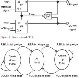
The Conventional PFD, which is shown in Figure 2, has the primary function as the NAND gate occupied by PFD, but the assignment state is different. Two D-Flip-flops (D = 1) with the clock signals are compared. Tristate Phase frequency detector finite state machine is shown in Figure 3.
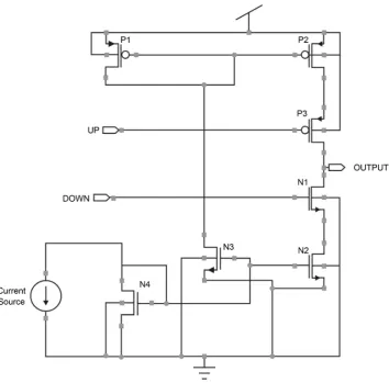
[image:3.595.244.505.434.691.2]The CP is nothing but the switching circuit used to generate dc voltages that are higher than the standard power supply. It is used to sink and source current into a loop filter based on the output of the phase frequency detector. The CP illustrated in Figure 4 converts the up and down signal pulses from PFD into current pulses as there are ca-pacitors in the loop filter. These current pulses change voltage drop on the loop filter impedance that is also the VCO control voltage. The CP design is mainly used to avoid the charge sharing effect. To minimize the effect caused by charge injection and clock
Figure 2. Conventional PFD.
Figure 4. Charge pump circuit.
feed-through, the current values of up and down signals are matched. Further, it is de-signed in such a way that there is no time mismatch between up and down signals, and finally low power consumption is achieved [11].
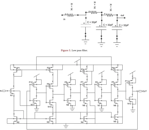
A Loop-filter is nothing but the Low Pass Filter (LPF) integrates error current to generate VCO control voltage and suppresses the noise and unwanted phase detector outputs. The filter shown in Figure 5 alters the ability of the loop to change frequencies instantly. If the filter has low cut off frequency, then the changes in tune voltage take place slowly. The VCO is unable to vary its frequency as soon, and this is due to the slow changes in the voltage level. Another important module in designing PLL is the VCO. A type of VCO called Ring Oscillator (RO) consists of some delay stages with a feedback system and to achieve the oscillation, the phase shift of 2π and unity voltage gain is required at the oscillating frequency.
Figure 5. Low pass filter.
Figure 6. Current starved VCO.
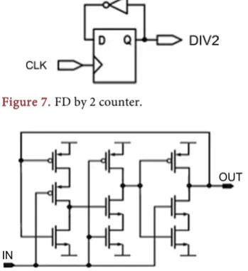
and the source voltage is applied to the gates of all the lower NMOS transistors [12]. The FD by 2 is the first simple counter, which is easier to configure the memories with flip-flops. The input signal’s frequency when fed to the FD circuit, it generates an output signal as half of the input frequency. Figure 7 illustrates the general structure of FD by 2.
used in the first stage of the PLL. Partition by 2/3 unit shown in Figure 9 consists of two toggle DFFs and additional logic gates. One way is used to reduce the delay and another is to reduce power consumption, where combining the logic gates and the FD 2/3 unit. The wideband 2/3 pre-scaler has the benefit of saving more than 50% of power during the divide-by-2 operation [14]. This paper reports a new proposal of a modified circuit for PFD in order to reduce the dead zone and combined with other modules to obtain PLL output. Further, the PLL characteristics are observed by adding two types of frequency dividers.
[image:6.595.43.565.184.688.2]The remainder of the paper is organized as follows; Section 2 briefs the proposed circuit and the design of other modules followed by the simulation results and discus-sion in Section 3 and finally ended with Concludiscus-sion in Section 4.
Figure 7. FD by 2 counter.
[image:6.595.287.462.251.442.2]Figure 8. FD using TSPC logic.
[image:6.595.45.552.469.683.2]2. Proposed PFD and the Other Modules Design
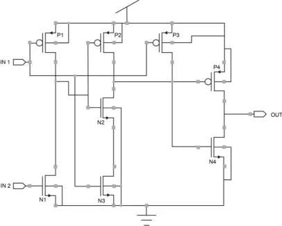
[image:7.595.144.551.364.689.2]From the Literature survey [7], it is observed that the internal signal routing is required to reduce the dead zone in the PFD circuit. Based on that concept, the high-speed dy-namic PFD is proposed (PPFD) and designed as shown in Figure 10. The reset path of PFD is eliminated by routing the PFD input connections to the flip-flop that is located next to it. The input of one flip-flop plays a role in developing reset signal for the other flip flop. Thereby the dead zone is eliminated and the power is decreased by reducing a transistor from the existing circuit of the High speed dynamic PFD [15]. Reducing the number of transistors, the area is decreased, and the speed of the circuit is increased. It overcomes the inaccuracy of the PFD output when the reference signal leads the VCO signal as the design is minimized. With the aid of smallest channel length in the circuit design, it confesses as an explicit device that is shrinking with the scaling of CMOS technology.
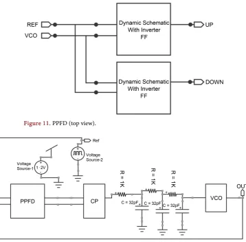
Figure 11 represents the top module of the PPFD. In PLL, the reference signal and the signal from the VCO are connected into the PPFD circuit. The result of the PPFD circuit is connected to the CP. The output of the CP is fed to the loop filter and finally it is applied to the VCO. The VCO frequency harmonizes to the in-out frequency of the loop. This process is a frequency pull in, and then the VCO phase is adjusted for the
input phase. This operation is said to be a Phase lock-in. After addition, the PLL achieves the phase-locked condition, where PLL tracks the input. Under this condition, VCO frequency is equal to the input frequency. The overall PLL design is presented in Figure 12.
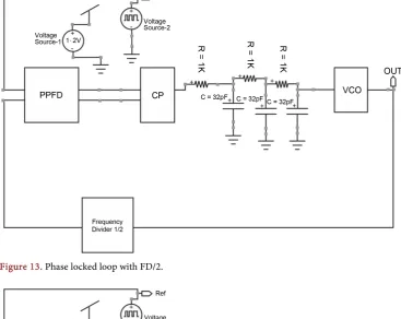
[image:8.595.190.549.339.691.2]PLL operation is repeated with every external input pulse so that the feedback VCO and the external input clock are matched, the circuit then locks onto itself within a narrow frequency band. If the clock of entry varies slightly, the PLL frequency does not change. This narrow frequency band is the dead zone of the PPFD. Within this zone, the VCO signal and reference signal are so close in-phase that there are no correction pulses out of the PPFD circuit. Once the phase shifts out of this frequency band, the PPFD is correcting again. As the PLL design is functioning properly, it is extended fur-ther by connecting with Frequency divider (FD) blocks. The FD performs the frequency division by a factor of 2 which is illustrated in Figure 13 where it will divide the phase of the input signal by 2 as well. Figure 14 shows PLL with FD by 2/3 counter. The Fre-quency divider takes an input signal of a freFre-quency and generates an output signal as 2/3 of the input frequency. The wideband single-phase clock 2/3 pre-scaler circuit con-sists of two D-flip-flops. In addition two NOR gates embedded in the Flip-flops. Here,
Figure 11. PPFD (top view).
Figure 13. Phase locked loop with FD/2.
Figure 14. Phase locked loop with FD 2/3.
the transistors in DFF helps to eliminate the short-circuit power during the FD by-2 operation. Logic signal MC controls the switching of division ratios.
3. Results and Discussion
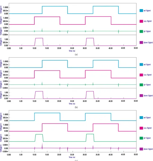
[image:9.595.183.552.344.581.2]The width and the length of the transistors for both the NMOS and PMOS are fixed as 0.5 µm and 0.18 µm respectively. The simulated output waveform satisfies all the essen-tial PFD criteria. The following simulated outputs show the PPFD’s performance with the dead zone as a constraint. Figure 15(b) waveform indicates that the reference signal
(a)
(b)
[image:10.595.44.553.135.670.2](c)
Figure 15. (a) PFD output waveforms when both reference and VCO signal are in phase. (b) PFD output waveforms when reference
leads the VCO signal by a delay of 3ns and the VCO signal leads the reference signal by a delay of 3ns as shown in Figure 15(c). Due to reset signal routing, PPFD is unable to detect the phase difference between two input signals even in phase with each other as illustrated in Figure 15(a).
In these graphs, a, b, c, d represent reference, VCO output, up and down signals (PFD Outputs) respectively. Here the input signals are varied as illustrated below and the dead zone is detected with the outputs obtained. It shows that the circuit produces output with zero dead zone. Since the circuit is verified with a low frequency operation, few small spikes for about peak to peak 5 mV is observed.
Decreasing the number of transistors in the reset path reduces the power from the existing one. Power dissipation of the PPFD for the supply voltage of 1.8 V is 85 pW and for 1.2 V is 40.8 pW. From the outputs it is observed that, the power supply dissi-pation is reduced with decrease in the supply voltage as expected due to the quadratic dependence on the supply voltage and also by the optimization of transistors both in width and gate length.
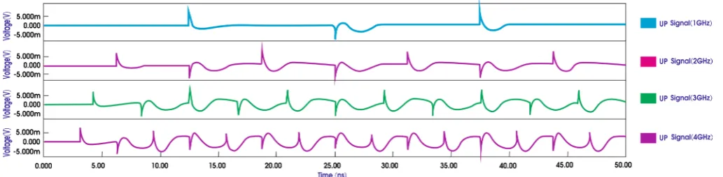
[image:11.595.42.559.559.686.2]Figure 16 represents the operation of the PPFD with one of the output signals (up signal) for various input frequencies ranging from 1 GHz to 4 GHz. There is a consis-tency in the simulated output irrespective of the variation in the speed of the input fre-quencies. Modified PPFD circuit operates properly for low to high frequency ranges with both 1.8 V and 1.2 V power supply and it is proved that the higher sensitivity, bet-ter the detection when the frequency is varied. It also effectively senses both the input rising and falling edges. As power supply is lowered, low power dissipation is achieved. Figure 17(a) shows that the top level simulation of the PLL. It shows clearly the signals of up and down with free of dead zone. In order to justify the PLL output, overall mod-ule is extended with two FDs such as divide by 2 and divide 2 by 3. The outputs of the circuits are shown in Figure 17(b) and Figure 17(c) respectively. To extend, Monte Carlo simulations are performed for about ten sweep values for all the three PLL mod-ules shown in Figures 18(a)-(c) respectively. The analysis is done based on variations of the threshold voltage in the 0.18 µm using T-Spice.
Table 1 illustrates the performance of the PPFD with preceding architectures. Even though most of the design has null dead zone, the number of transistors has been reduced.
(a)
(b)
[image:12.595.46.553.68.490.2](c)
Figure 17. (a) Phase locked loop output with zero deadlock condition. (b) Phase locked loop output with divide by 2 counter. (c) Phase
locked loop output with divide by 2/3 counter.
Fan et al. constructed PFD [16] with a power dissipation of 3 mW but uses digital
cir-cuitry for which the value is high. It even occupies large area on the chip as a result of the error amplifier circuitry. Hsu et al. designed PFD architectures [17] with smaller device sizes to reduce the power dissipation. Chen et al. designed PFD [18] with still lowering power dissipation by re-routing. Thakore et al. designed a PFD [19] that pro-duces a power dissipation of 870 pW with 1.2 V power supply. Is mail et al. designed a PFD [20] with less number of transistor count, but it has limitation in detecting the in-put phase difference as the detection works on inin-puts negative edge of the reference signal. The proposed work gives a still lower power dissipation of 85 pW at 1.8 V and 40.8 pW at 1.2 V due to internal signal re-routing.
(a)
(b)
[image:13.595.43.553.66.621.2](c)
Figure 18. (a) Monte Carlo Simulation result of phase locked loop output. (b) Monte Carlo Simulation result of phase locked loop
with divide by 2 counter output. (c) Monte Carlo Simulation result of phase locked loop with divide by 2/3 counter output.
Table 1. Comparison with previous work.
Reference
Paper Process CMOS Power supply (V) dissipation (W) Total power Reference frequency (MHz) Dead Zone (ps) Transistor Count
[2] 0.18 µm 1.8 6.6 µ 50 0 12
[8] 0.18 µm 1.8 - 10 - 25 120 24 [9] 0.18 µm 1.8 870 p 50 - 100 2 18
[13] 0.18 µm 1.8 3 m 50 0 24
[15] 0.18 µm 1.8 1.56 m 50 - 22
[17] 0.18 µm 1.8 118 p 50 0 18
1.2 59 p
This work 0.18 µm 1.8 85 p 50 - 100 0 16 1.2 40.8 p
Table 2. Comparison of power.
Module Average Power Consumed (µW)
PLL 2.48
PLL with divide by 2 1.53 PLL with divide by 2/3 0.65
Further using the measurement results from Monte Carlo simulations, Power com-parison is done for all the three PLL modules shown in Figures 19(a)-(c) respectively. Each graph represents the value of the power corresponding to its sweep value. Since number of transistors is reduced, area is minimised and such low power consumption is achieved.
4. Conclusion
[image:14.595.190.553.305.373.2](a)
(b)
[image:15.595.138.556.59.660.2](c)
Figure 19. (a) Comparison of power in Monte Carlo Simulation result of the PLL. (b) Comparison of power in
Acknowledgements
Author would like to thank Dr. H. Mangalam, Professor, Department of Electronics & Communication Engineering, Sri Ramakrishna Institute of Technology, Coimbatore, India for providing immense support and encouragement at all levels.
References
[1] Best, R.E. (2003) Introduction to PLLs, Phase-Locked Loops: Design, Simulation and Ap-plications. 5th Edition, Chapter 1, Buch McGraw-Hill, New York.
[2] Banerjee, D. (2006) PLL Performance, Simulation and Design. Dog Ear Publishing, LLC, IN, USA.
[3] Nakamura, K., et al. (1998) A 6 Gb/s CMOS Phase Detecting DEMUX Module Using Half- Frequency Clock. Digest of Symposium on VLSI Circuits, 196-197.
[4] Alexander, J. (1975) Clock Recovery from Random Binary Signals. Electronics Letters, 11, 541-542. http://dx.doi.org/10.1049/el:19750415
[5] Hogge Jr., C.R. (1985) A Self Correcting Clock Recovery Circuit. IEEE Journal of Lightwave Technology, 3, 1312-1314. http://dx.doi.org/10.1109/JLT.1985.1074356
[6] Chen, W.H., Inerowicz, M.E. and Jung, B. (2010) Phase Frequency Detector with Minimal Blind Zone for Fast Frequency Acquisition. IEEE Transactions on Circuits and Systems-II: Express Briefs, 57, 936-940.
[7] Mansuri, M., Liu, D., Yang, C.K. (2002) Fast Frequency Acquisition Phase Frequency De-tectors for Gsamples/s Phase-Locked Loops. IEEE Journal Solid-State Circuits, 37, 1331- 1334. http://dx.doi.org/10.1109/JSSC.2002.803048
[8] Minhad, K.N., Reaz, M.B.I. and Jalil, J. (2014) A Low Power 0.18 µm CMOS Phase Fre-quency Detector for High Speed PLL. Elektronika IR Electronika, 20, 29-34.
[9] Soh, L.K., Sulaiman, M.S. and Yusof, Z. (2008) A Fast Lock Delay-Locked Loop Architec-ture with Improved Precharged PFD. Journal of Analog Integrated Circuits Signal Process, 55, 149-154. http://dx.doi.org/10.1007/s10470-008-9131-7
[10] Anushkannan, N.K. and Mangalam, H. (2015) Design of a CMOS PFD-CP Module for a PLL. Sadhana, 40, 1105-1116. http://dx.doi.org/10.1007/s12046-015-0379-1
[11] Singh, Y.P. and Chauhan, R.K. (2013) Fast Charge Pump Circuit for PLL Using 50 nm CMOS Technology. International Journal of Advanced Research in Computer and Com-munication Engineering, 2, 2616-2619.
[12] Jacob Baker, R., Li, H. and David Boyce, E. (2000) CMOS Circuit Design, Layout and Simulation. IEEE Press Series on Microelectronics Systems, Piscataway, 355-361, 383-387. [13] Pellegrino, S., Levantino, S., Samori, C. and Lacaita, A.L. (2004) A 13.5-mW 5-GHz
Fre-quency Synthesizer with Dynamic-Logic FreFre-quency Divider. IEEE Journal of Solid-State Circuits, 39, 378-383. http://dx.doi.org/10.1109/JSSC.2003.821784
[14] Manthena, V.K., et al. (2012) A Low-Power Single-Phase Clock Multiband Flexible Divider. IEEE Transactions on Very Large Scale Integration Systems, 20, 376-380.
http://dx.doi.org/10.1109/TVLSI.2010.2100052
[15] Kim, S., Lee, K., Moon, Y., Jeong, D.K., Choi, Y. and Lim, H.K. (1997) A 960 Mb/s/pin In-terface for Skew-Tolerant Bus Using Low Jitter PLL. IEEE Journal of Solid-State Circuits, 32, 691-700. http://dx.doi.org/10.1109/4.568836
Millimeter Wave Wireless Technology and Applications, Nanjing, 18-20 September 2012, 1-4.
[17] Hsu, C.W., Karthik, T., Yu, S.A. and Peter, R.K. (2011) A 2.2 GHz PLL Using a Phase-Fre- quency Detector with an Auxiliary Sub-Sampling Phase Detector for in-Band Noise Sup-pression. Proceedings of IEEE Custom Integrated Circuits Conference,San Jose, 19-21 Sep- tember 2011, 1-4.
[18] Chen, R.Y. and Chen, W.Y. (2007) A High-Speed Fast-Acquisition CMOS Phase/Frequency Detector for MB-OFDM UWB. IEEE Transactions on Consumer Electronics, 53, 23-26.
http://dx.doi.org/10.1109/TCE.2007.339496
[19] Thakore, K.P., Parmar, H.C. and Devashrayee, N.M. (2011) Low Power and Low Jitter Phase Frequency Detector for Phase Lock Loop. International Journal of Engineering Science and Technology, 3, 1998-2004.
[20] Ismail, N.M.H. and Othman, M. (2009) A Simple CMOS PFD for High Speed Applications. European Journal of Scientific Research, 33, 261-269.
Submit or recommend next manuscript to SCIRP and we will provide best service for you:
Accepting pre-submission inquiries through Email, Facebook, LinkedIn, Twitter, etc. A wide selection of journals (inclusive of 9 subjects, more than 200 journals)
Providing 24-hour high-quality service User-friendly online submission system Fair and swift peer-review system
Efficient typesetting and proofreading procedure
Display of the result of downloads and visits, as well as the number of cited articles Maximum dissemination of your research work